A Non-Dissipative Equalizer with Fast Energy Transfer Based on Adaptive Balancing Current Control †


Abstract
1. Introduction
2. Operating Principle and Design of Equalizer Power Stage
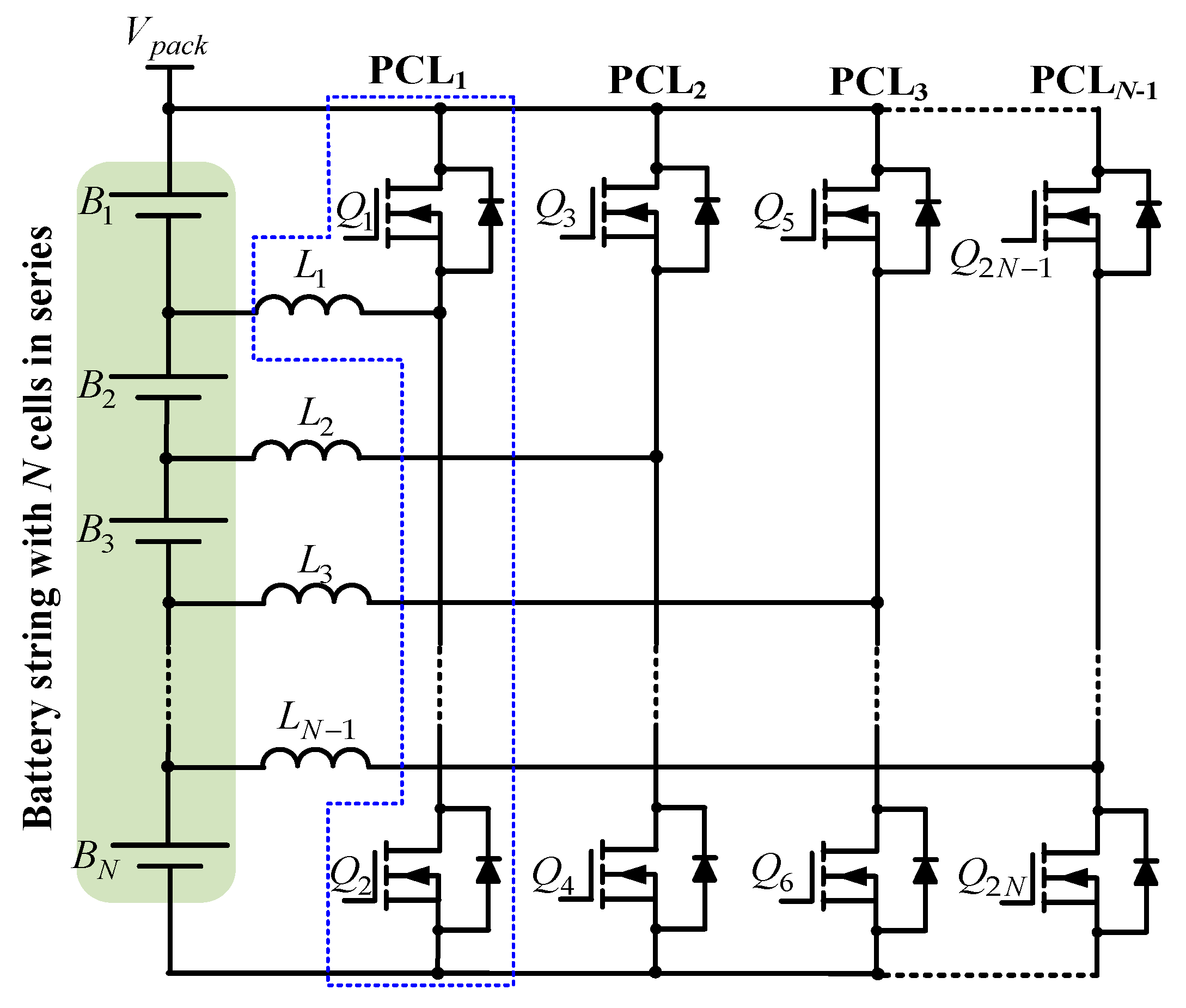
2.1. Topology of the Power Stage Studied
2.2. Operating Principle
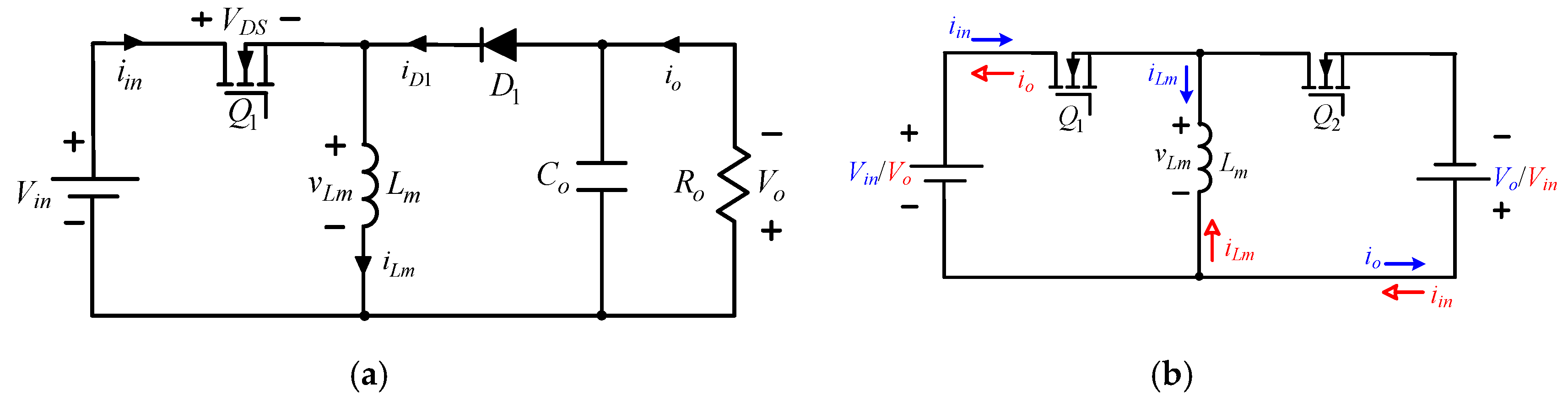
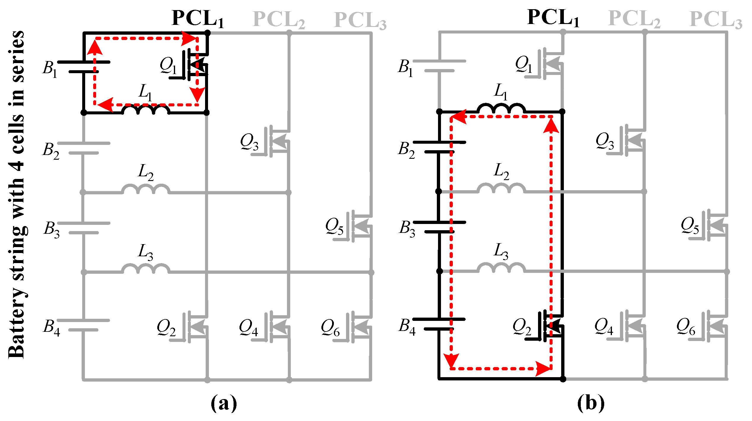
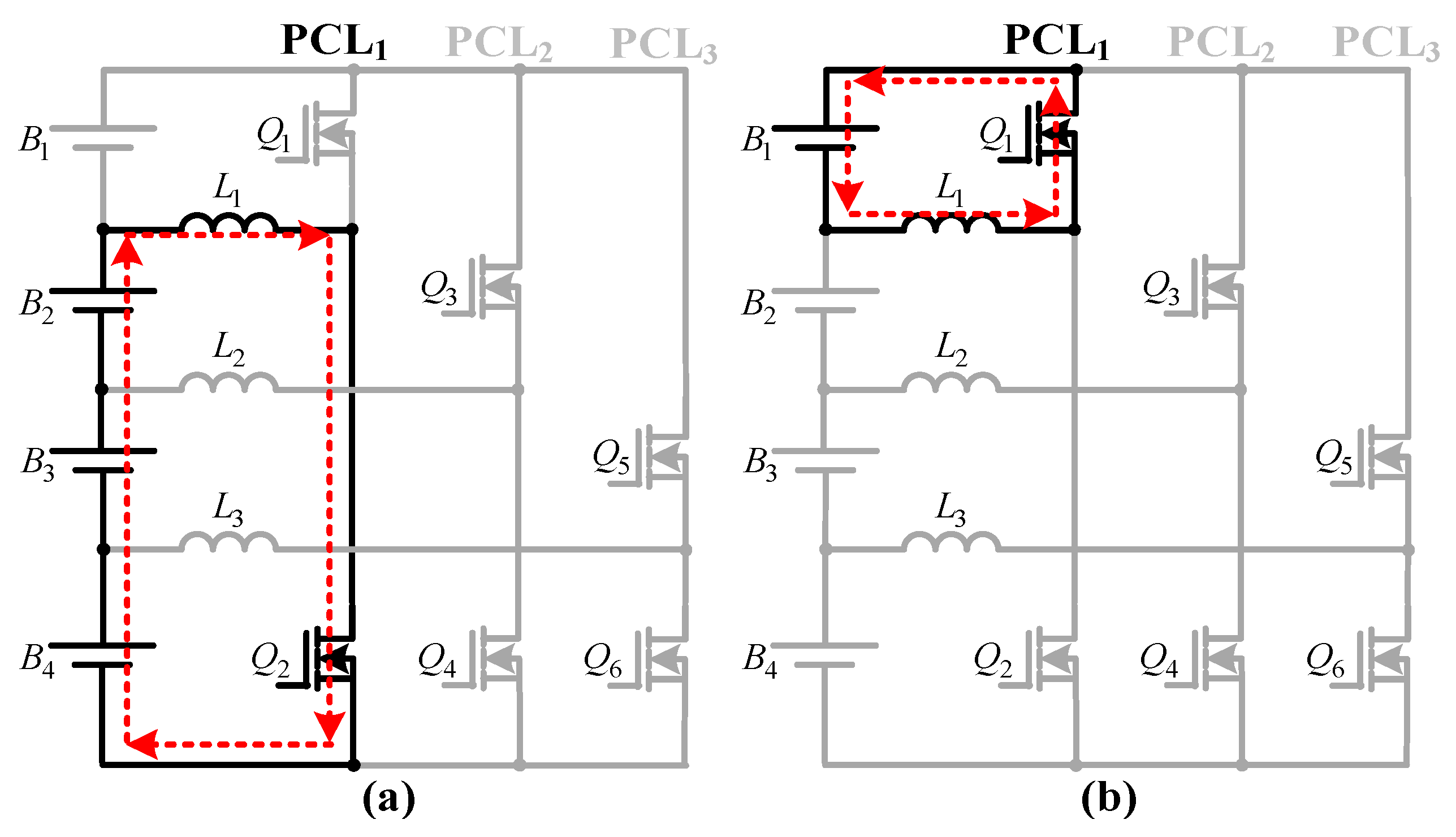
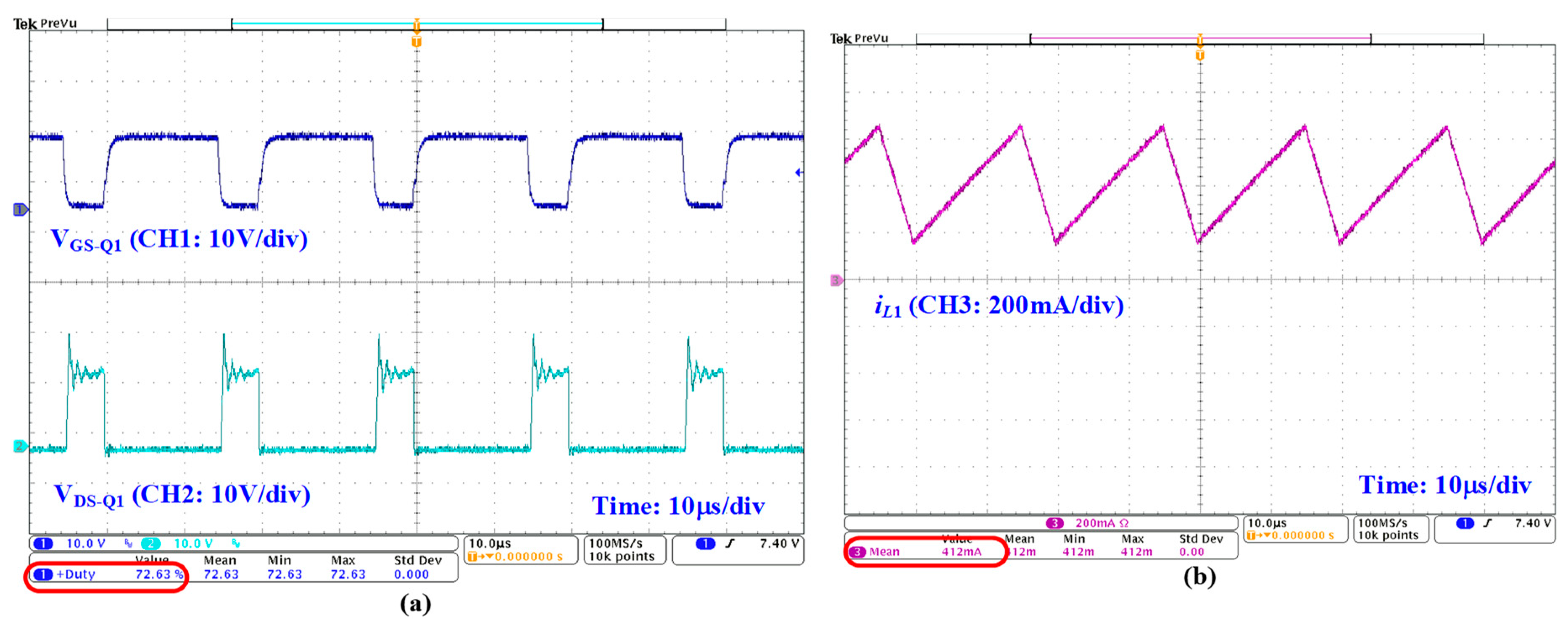
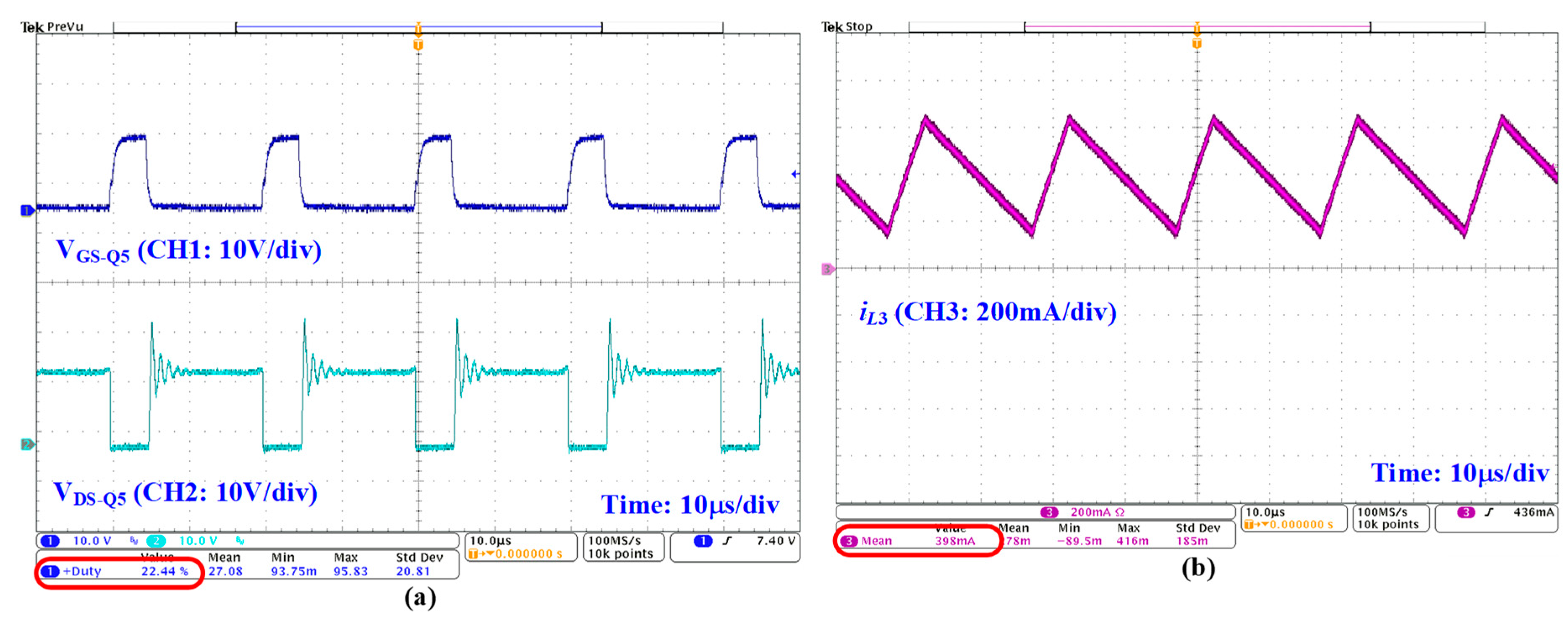
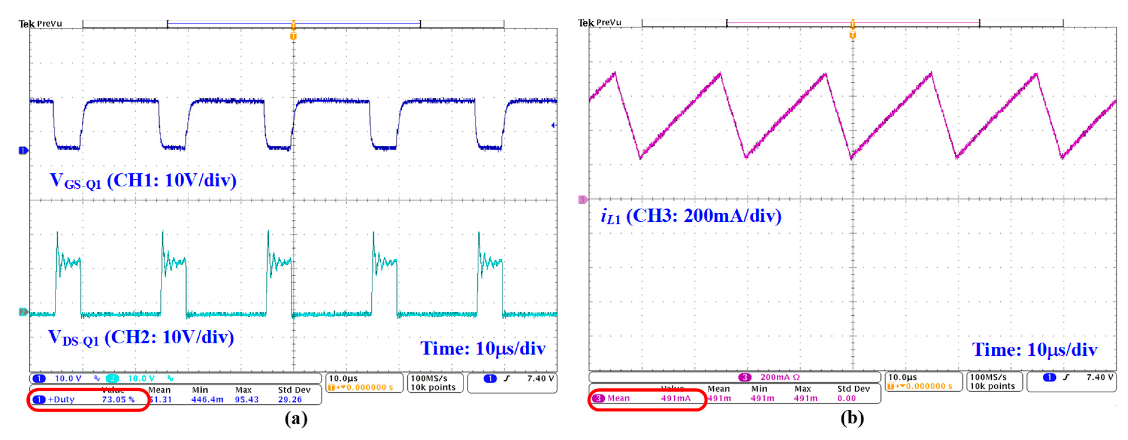
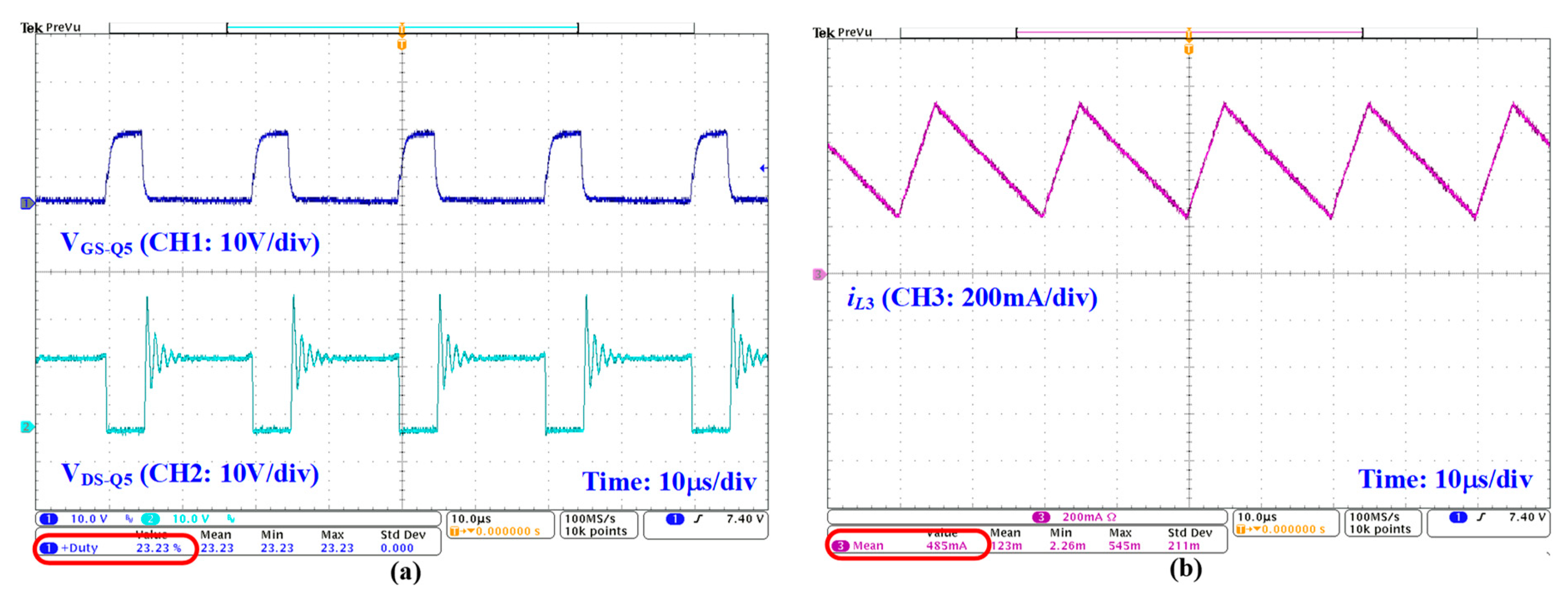
- C2SP or SP2C mode: From Figure 1, it can be observed that cell B1 and sub-pack B2-B3-B4 can transfer energy to each other bidirectionally to achieve the C2SP or SP2C balancing mode through the PCL1, which is formed by the Q1, Q2, and L1. When the average voltage of the sub-pack B2-B3-B4 is less than the voltage of cell B1, C2SP mode is activated. The PCL1 is operated in boost mode to step up the cell voltage for output voltage regulation and releases its energy to charge the sub-pack through the inductor L1. Figure 3a shows the equivalent circuit (EC) operated in subinterval 1, the switch Q1 is turned on, Q2 is turned off, and the B1 energizes the L1. In subinterval 2, the Q2 is turned on and Q1 is turned off, and the EC is shown in Figure 3b. At this time, the energy stored in L1 in the former subinterval is transferred to the sub-pack. This C2SP mode mainly modulates the duty cycle of Q1, the duty cycle of Q2 is complementary to Q1 and a proper dead time must be added to promise correct operation and avoid failure. On the other hand, when the average voltage of the sub-pack is more than the B1 voltage, the SP2C mode is actuated and the PCL1 is operated in buck mode to step down the sub-pack voltage for output voltage regulation and releases its energy to charge the cell B1. The operation flow of SP2C balance mode is opposite to C2SP mode, i.e., when in subinterval 1 operation, the switch Q2 is turned on and Q1 is turned off, and the sub-pack energizes L1. The EC, as shown in Figure 4a, illustrates the energy flowing in this subinterval. Figure 4b shows the EC operated in subinterval 2, the switch Q2 is turned off and Q1 is turned on. At this time, the energy stored in L1 in the previous subinterval is released to charge B1 to complete the energy conversion. In SP2C mode, the duty cycle of Q2 is modulated dominantly to maintain the correct process. The duty cycle of Q1 is complementary to Q2, and an appropriate dead time should also be inserted to avoid breakdown. Similarly, in this four-cell example, the SP2C or C2SP balance mode can also be done by the PCL3, which is constituted by the Q5, Q6, and L3, to transfer energy to each other bidirectionally between the sub-pack B1-B2-B3 and cell B4. The operating principle and analysis method are the same as that described above, so it will not be repeated.
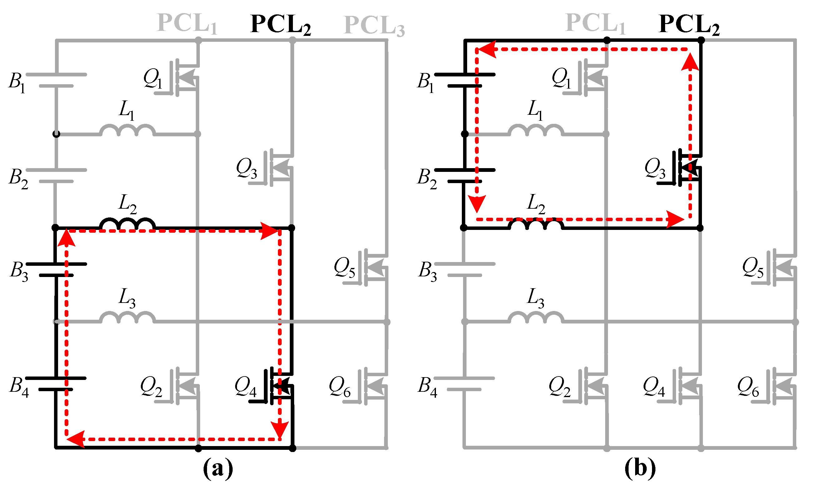
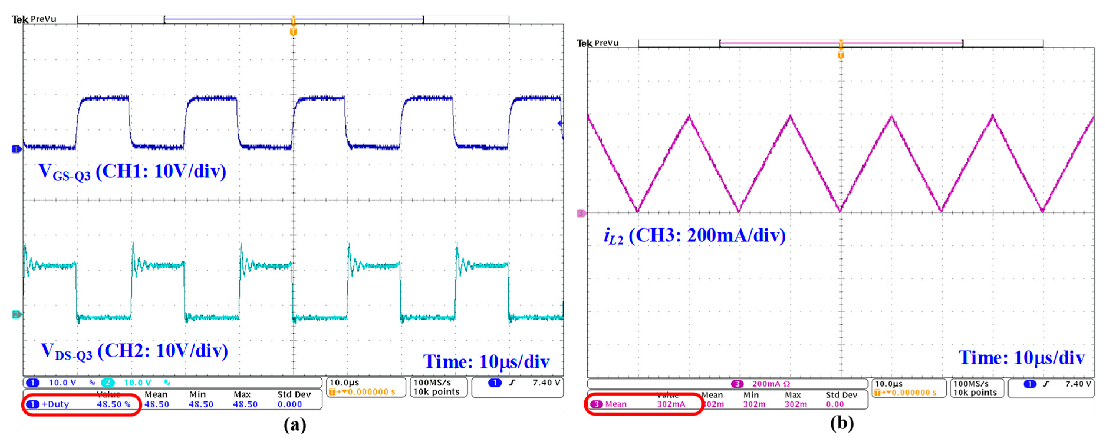
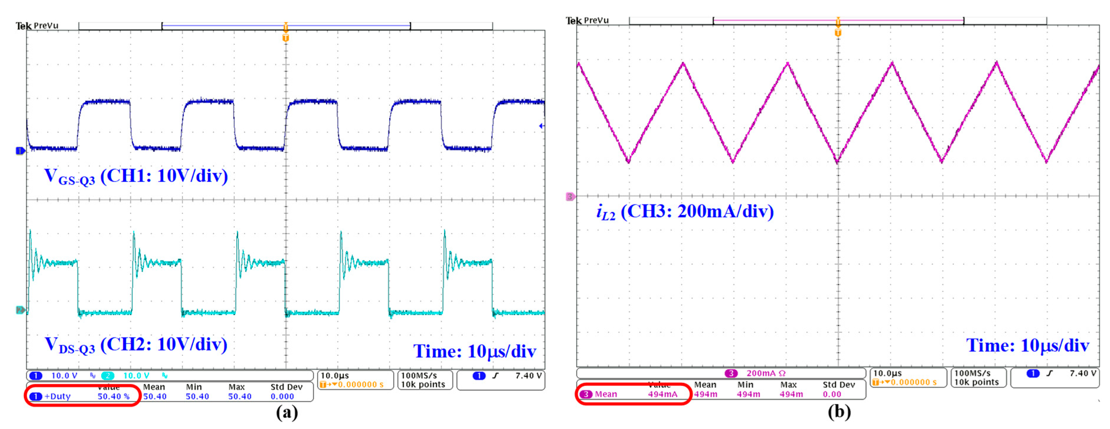
- SP2SP mode: The energy stored in sub-pack B1-B2 or sub-pack B3-B4 can be transferred to each other through the bidirectional PCL2 constructed by the Q3, Q4, and L2 to achieve the SP2SP balance mode. When the average voltage of sub-pack B3-B4 is more than that of sub-pack B1-B2, SP2SP mode is triggered and the sub-pack B3-B4 releases its energy, through the inductor L2 for energy exchange, to charge the other side sub-pack B1-B2. Figure 5a shows the EC operated in subinterval 1 in SP2SP mode, the switch Q4 is turned on and Q3 is turned off, and the B3-B4 energizes the inductor L2. In subinterval 2, the switch Q3 is turned on and Q4 is turned off, and the EC is shown in Figure 5b. At this time, the energy stored in L2 in the previous subinterval is released to charge the sub-pack B1-B2. In this SP2SP mode, the duty cycle of Q4 is modulated mainly to dominate the energy conversion exactly. The duty cycle of Q3 is regulated complementarily with Q4, and a good dead time should be added to the switching period to achieve correct circuit operation and avoid malfunction. On the other hand, in the situation that the average voltage of the sub-pack B3-B4 is less than that of the sub-pack B1-B2, the SP2SP mode is still asserted, but in turn, the sub-pack B1-B2 discharges to energize the other side sub-pack B3-B4 through the control of PCL2. Basically, the operating principles and analysis manners of these two balance modes are exactly the same as those mentioned above, except for the interchange of the input and output voltages and the main switch of regulating the duty cycle of the PCL2, so it will not be described again.
2.3. Parameter Design of Key Components
3. Equalizer System Configuration and Balance Strategy
3.1. System Configuration
3.2. Derivation of Balance Strategy
3.2.1. Balance Strategy for the FDC Method
3.2.2. Balance Strategy for the AVDC Method
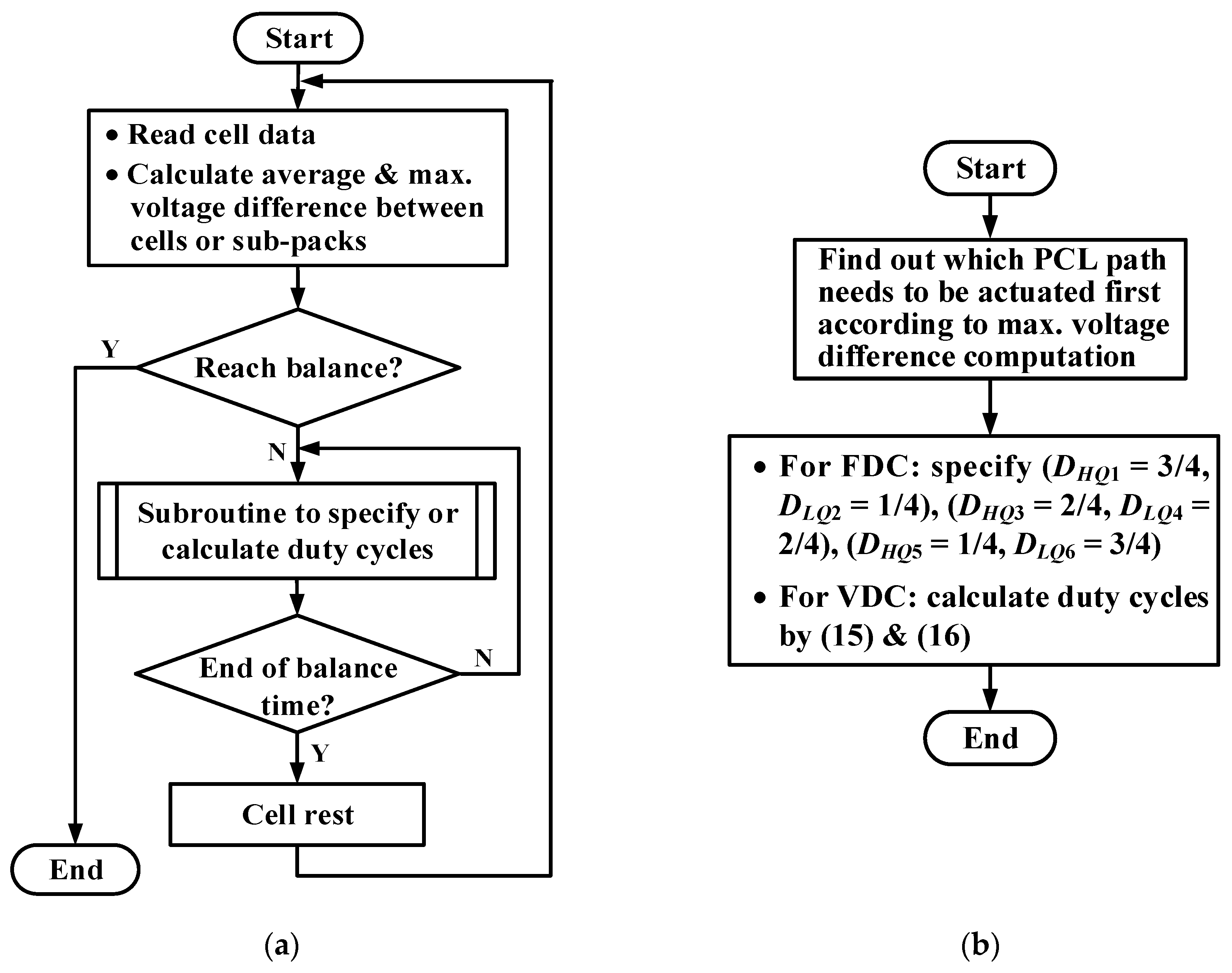
3.2.3. Operating Flowchart of Balance Algorithm
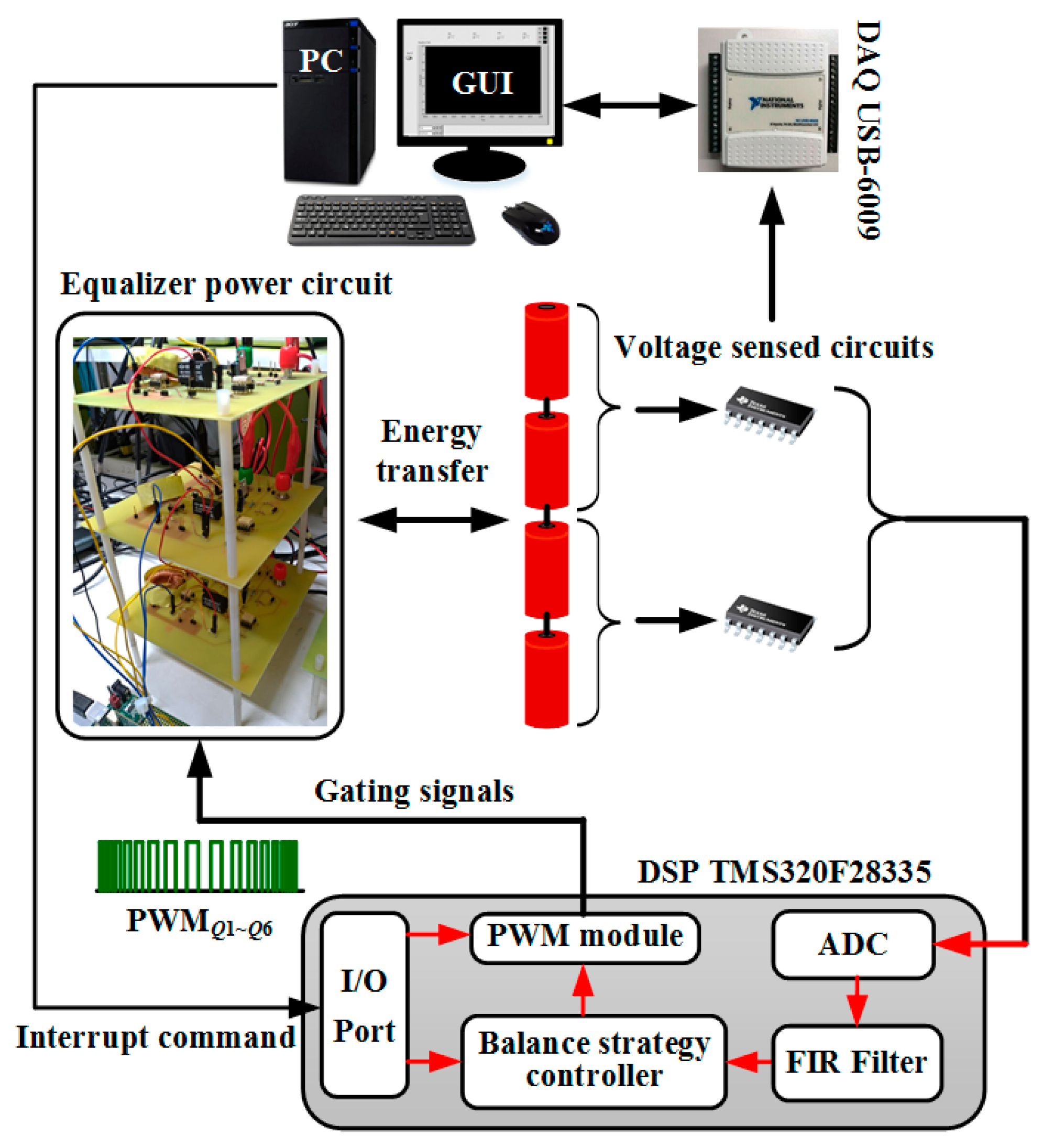
4. Experimental Results and Comparisons
4.1. Simulation Results
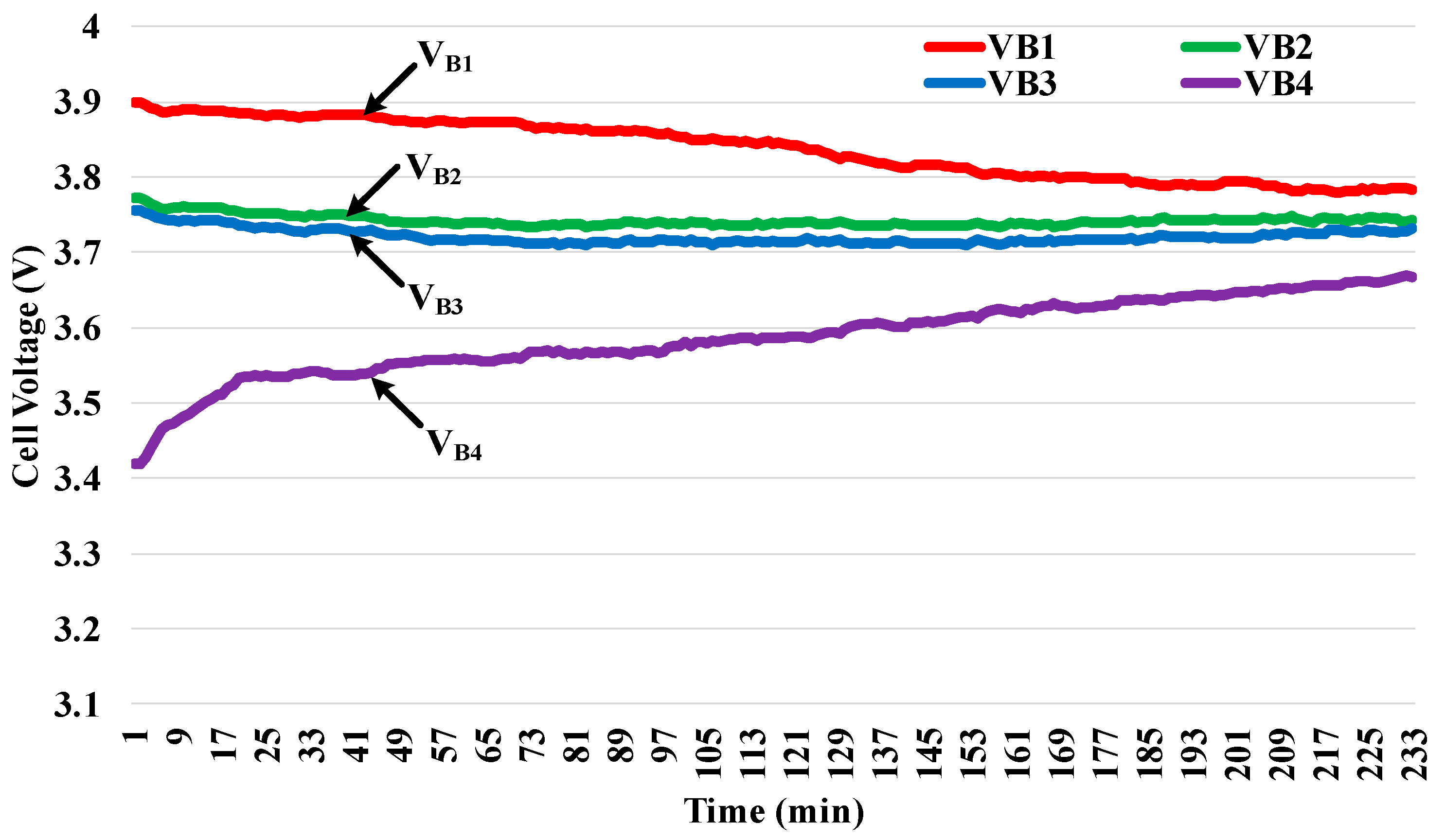
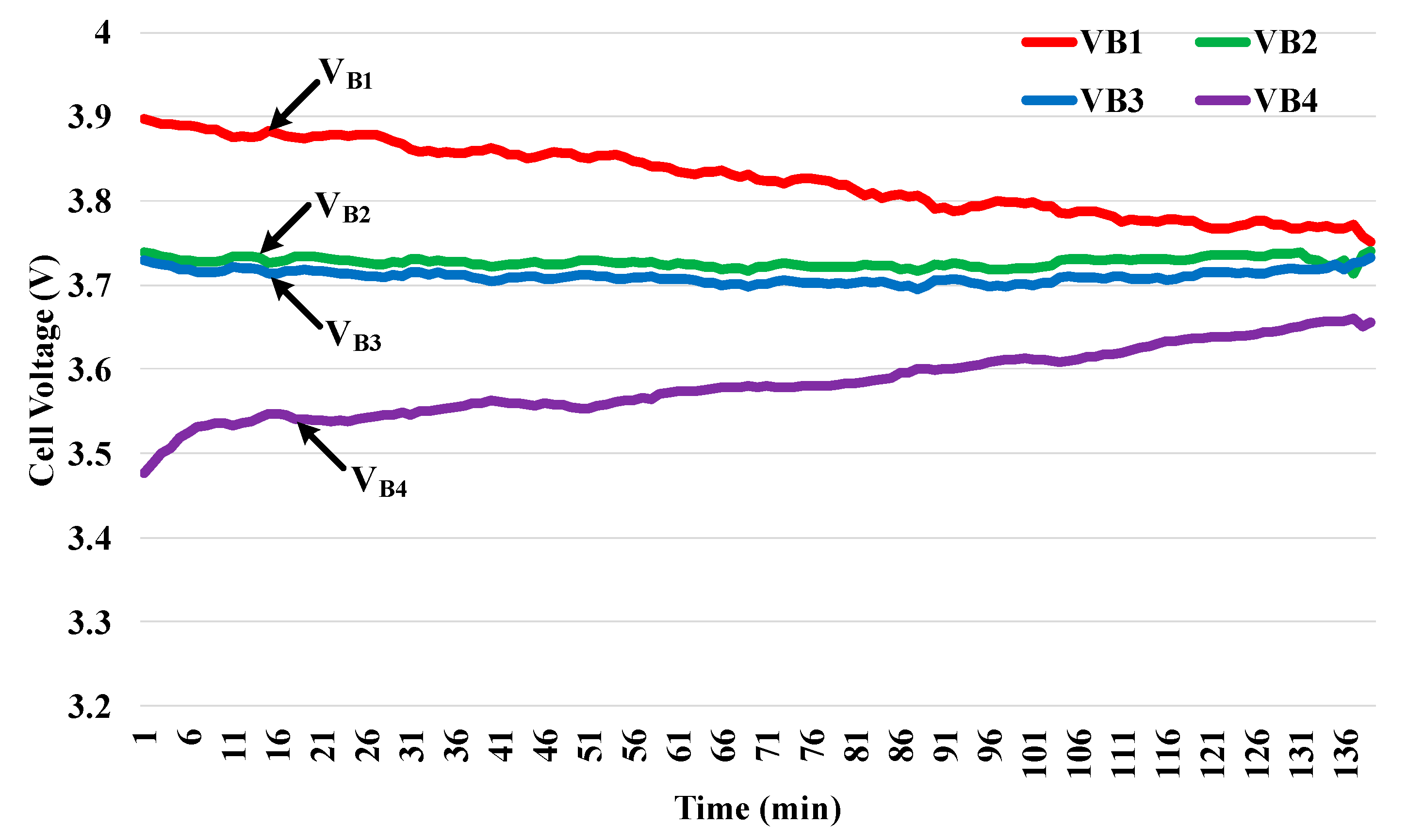
4.2. Experimental Results
4.3. Cpmparison and Discussion on Experimental Results
5. Conclusions
Author Contributions
Funding
Conflicts of Interest
References
- Kwon, S.J.; Lee, S.E.; Lim, J.H.; Choi, J.; Kim, J. Performance and Life Degradation Characteristics Analysis of NCM LIB for BESS. Electronics 2018, 7, 406. [Google Scholar] [CrossRef]
- Barchi, G.; Pierro, M.; Moser, D. Predictive Energy Control Strategy for Peak Shaving and Shifting Using BESS and PV Generation Applied to the Retail Sector. Electronics 2019, 8, 526. [Google Scholar] [CrossRef]
- Go, S.; Choi, J. Design and Dynamic Modelling of PV-Battery Hybrid Systems for Custom Electromagnetic Transient Simulation. Electronics 2020, 9, 1651. [Google Scholar] [CrossRef]
- Montoya, O.; Gil-González, W.; Serra, F.; Hernández, J.; Molina-Cabrera, A. A Second-Order Cone Programming Reformulation of the Economic Dispatch Problem of BESS for Apparent Power Compensation in AC Distribution Networks. Electronics 2020, 9, 1677. [Google Scholar] [CrossRef]
- Dimitrov, B.; Krishna, M.; Cruden, A.; Sharkh, S.; Elkhateb, A. Analysis, Design, and Experimental Validation of a Primary Side Current-Sensing Flyback Converter for Use in a Battery Management System. Electronics 2018, 7, 43. [Google Scholar] [CrossRef]
- Ali, M.; Zafar, A.; Nengroo, S.; Hussain, S.; Kim, H. Effect of Sensors Sensitivity on Lithium-Ion Battery Modeled Parameters and State of Charge: A Comparative Study. Electronics 2019, 8, 709. [Google Scholar] [CrossRef]
- Zheng, Y.; He, F.; Wang, W. A Method to Identify Lithium Battery Parameters and Estimate SOC Based on Different Temperatures and Driving Conditions. Electronics 2019, 8, 1391. [Google Scholar] [CrossRef]
- Aiello, O. Electromagnetic Susceptibility of Battery Management Systems’ ICs for Electric Vehicles: Experimental Study. Electronics 2020, 9, 510. [Google Scholar] [CrossRef]
- Kim, J.; Shin, J.; Chun, C.; Cho, B.H. Stable Configuration of a Li-ion Series Battery Pack Based on a Screening Process for Improved Voltage/SOC Balancing. IEEE Trans. Power Electron. 2012, 27, 411–424. [Google Scholar] [CrossRef]
- Chatzakis, J.; Kalaitzakis, K.; Voulgaris, N.C.; Manias, S.N. Designing a New Generalized Battery Management System. IEEE Trans. Ind. Electron. 2013, 50, 990–999. [Google Scholar] [CrossRef]
- Lv, J.; Song, W.; Lin, S.; Chen, M.; Feng, Z.; Li, Y.; Ding, Y. Influence of Equalization on LiFePO4 Battery Inconsistency. Int. J. Energy Res. 2017, 41, 1171–1181. [Google Scholar] [CrossRef]
- Samadani, E.; Mastali, M.; Farhad, S.; Fraser, R.A.; Fowler, M. Li-ion Battery Performance and Degradation in Electric Vehicles under Different Usage Scenarios. Int. J. Energy Res. 2016, 40, 379–392. [Google Scholar] [CrossRef]
- Kabir, M.M.; Demirocak, D.E. Degradation Mechanisms in Li-ion Batteries: A state-of-the-art Review. Int. J. Energy Res. 2017, 41, 1963–1986. [Google Scholar] [CrossRef]
- Lu, L.; Han, X.; Li, J.; Hua, J.; Ouyang, M. A Review on the Key Issues for Lithium-ion Battery Management in Electric Vehicles. J. Power Sources 2013, 226, 272–288. [Google Scholar] [CrossRef]
- Lai, X.; Jiang, C.; Zheng, Y.; Gao, H.; Huang, P.; Zhou, L. A Novel Composite Equalizer Based on an Additional Cell for Series-Connected Lithium-Ion Cells. Electronics 2018, 7, 366. [Google Scholar] [CrossRef]
- Shi, F.; Song, D. A Novel High-Efficiency Double-Input Bidirectional DC/DC Converter for Battery Cell-Voltage Equalizer with Flyback Transformer. Electronics 2019, 8, 1426. [Google Scholar] [CrossRef]
- Farzan Moghaddam, A.; Van den Bossche, A. Forward Converter Current Fed Equalizer for Lithium Based Batteries in Ultralight Electrical Vehicles. Electronics 2019, 8, 408. [Google Scholar] [CrossRef]
- Wu, S.T.; Chang, Y.N.; Chang, C.Y.; Cheng, Y.T. A Fast Charging Balancing Circuit for LiFePO4 Battery. Electronics 2019, 8, 1144. [Google Scholar] [CrossRef]
- Pham, V.; Duong, V.; Choi, W. A Low Cost and Fast Cell-to-Cell Balancing Circuit for Lithium-Ion Battery Strings. Electronics 2020, 9, 248. [Google Scholar] [CrossRef]
- Farzan Moghaddam, A.; Van den Bossche, A. An Efficient Equalizing Method for Lithium-Ion Batteries Based on Coupled Inductor Balancing. Electronics 2019, 8, 136. [Google Scholar] [CrossRef]
- Uno, M.; Ueno, T.; Yoshino, K. Cell Voltage Equalizer Using a Selective Voltage Multiplier with a Reduced Selection Switch Count for Series-Connected Energy Storage Cells. Electronics 2019, 8, 1303. [Google Scholar] [CrossRef]
- Carter, J.; Fan, Z.; Cao, J. Cell Equalization Circuits: A Review. J. Power Sources. 2020, 448, 1–9. [Google Scholar] [CrossRef]
- Gallardo-Lozano, J.; Romero-Cadaval, E.; Milanes-Montero, M.I.; Guerrero-Martinez, M.A. Battery Equalization Active Methods. J. Power Sources. 2014, 246, 934–949. [Google Scholar] [CrossRef]
- Daowd, M.; Omar, N.; Van Den Bossche, P.; Van Mierlo, J. Passive and Active Battery Balancing Comparison Based on MATLAB Simulation. IEEE Veh. Power Propuls. Conf. 2011, 1–7. [Google Scholar] [CrossRef]
- Baronti, F.; Roncella, R.; Saletti, R. Performance Comparison of Active Balancing Techniques for Lithium-ion Batteries. J. Power Sources 2014, 267, 603–609. [Google Scholar] [CrossRef]
- Einhorn, M.; Roessler, W.; Fleig, J. Improved Performance of Serially Connected Li-ion Batteries with Active Cell Balancing in Electric Vehicles. IEEE Trans. Veh. Technol. 2011, 60, 2448–2457. [Google Scholar] [CrossRef]
- Ye, Y.; Cheng, K.W.C. An Automatic Switched-Capacitor Cell Balancing Circuit for Series-Connected Battery Strings. Energies 2016, 9, 138. [Google Scholar] [CrossRef]
- Kim, M.-Y.; Kim, C.-H.; Kim, J.H.; Moon, G.-W. A Chain Structure of Switched Capacitor for Improved Cell Balancing Speed of Lithium-ion Batteries. IEEE Trans. Ind. Electron. 2014, 61, 3989–3999. [Google Scholar] [CrossRef]
- Einhorn, M.; Guertlschmid, W.; Blochberger, T.; Kumpusch, R.; Permann, R.; Conte, F.V.; Kral, C.; Fleig, J. A Current Equalization Method for Serially Connected Battery Cells Using a Single Power Converter for Each Cell. IEEE Trans. Veh. Technol. 2011, 60, 4227–4237. [Google Scholar] [CrossRef]
- Imtiaz, A.M.; Khan, F.H. Time Shared Flyback Converter Based Regenerative Cell Balancing Technique for Series Connected Li-ion Battery Strings. IEEE Trans. Power Electron. 2013, 28, 5960–5975. [Google Scholar] [CrossRef]
- Lee, Y.-S.; Tsai, C.-E.; Ko, Y.-P.; Cheng, M.-W. Charge Equalization Using Quasi-Resonant Converters in Battery String for Medical Power Operated Vehicle Application. In Proceedings of the 2010 International Power Electronics Conference—ECCE ASIA, Sapporo, Japan, 21–24 June 2010; pp. 2722–2728. [Google Scholar]
- Lee, Y.S.; Chen, G.T. Quasi-Resonant Zero-Current-Switching Bidirectional Converter for Battery Equalization Applications. IEEE Trans. Power Electron. 2006, 21, 1213–1224. [Google Scholar] [CrossRef]
- Cassani, P.A.; Williamson, S.S. Design, Testing, and Validation of a Simplified Control Scheme for a Novel Plug-In Hybrid Electric Vehicle Battery Cell Equalizer. IEEE Trans. Ind. Electron. 2010, 57, 3956–3962. [Google Scholar] [CrossRef]
- Farzan Moghaddam, A.; Van den Bossche, A. Flyback Converter Balancing Technique for Lithium Based Batteries. Int. Conf. Mod. Circuits Syst. Technol. 2019, 1–4. [Google Scholar] [CrossRef]
- Lim, C.S.; Lee, K.J.; Ku, N.J.; Hyun, D.S.; Kim, R.Y. A Modularized Equalization Method Based on Magnetizing Energy for a Series-Connected Lithium-ion Battery String. IEEE Trans. Power Electron. 2014, 29, 1791–1799. [Google Scholar] [CrossRef]
- Kim, C.H.; Kim, M.Y.; Moon, G.W. A Modularized Charge Equalizer Using a Battery Monitoring IC for Series-Connected Li-ion Battery Strings in Electric Vehicles. IEEE Trans. Power Electron. 2013, 28, 3779–3787. [Google Scholar] [CrossRef]
- Zhang, Z.; Gui, H.; Gu, D.J.; Yang, Y.; Ren, X. A Hierarchical Active Balancing Architecture for Lithium-ion Batteries. IEEE Trans. Power Electron. 2017, 32, 2757–2768. [Google Scholar] [CrossRef]
- Feng, F.; Hu, X.; Liu, J.; Lin, X.; Liu, B. A Review of Equalization Strategies for Series Battery Packs: Variables, Objectives, and Algorithms. Renew. Sust. Energy Rev. 2019, 116, 1–18. [Google Scholar] [CrossRef]


| Items | Value |
|---|---|
| Nominal capacity (25 °C) | 2600 mAh |
| Nominal voltage | 3.7 V |
| Maximum continuous discharge current/Discharge cut-off voltage | 2.5 A/3.0 V |
| Energy density | Volumetric: 535 Wh/L Gravimetric: 193 Wh/kg |
| Temperature | Charge: 0 to +45 °C Discharge: −20 to +60 °C |
| Items | Value/Part Number |
|---|---|
| Inductance (Lm) | 16 μH |
| MOSFET-related parameters | IPP030N10N |
| On resistance (RDS(on)/RQi) | 3 mΩ |
| Output capacitance (COSS) | 1210 pF |
| Switching frequency (fs) | 50 kHz |
| Dead time | 1 μs |
| Item | Before Balance | After Balance | Balance Time | |||||
|---|---|---|---|---|---|---|---|---|
| Method | Vmax | Vmin | ΔVdiff,max | Vmax | Vmin | ΔVdiff | ||
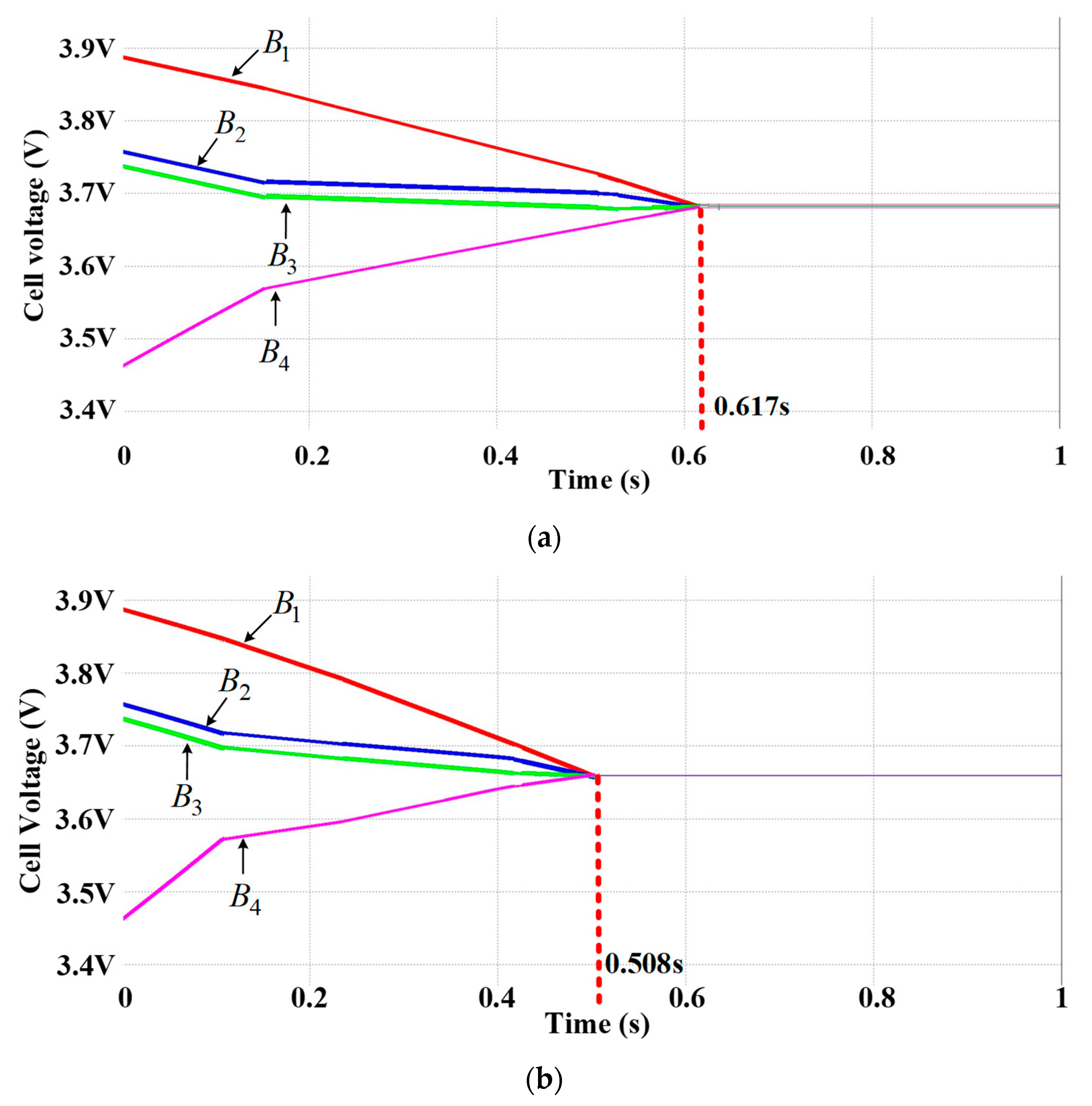
| FDC | 3.89 V | 3.46 V | 430 mV | 3.68 V | 3.67 V | 10 mV | 0.617 s | |
| AVDC | 3.89 V | 3.46 V | 430 mV | 3.66 V | 3.65 V | 10 mV | 0.508 s | |
| Item | Before Balance | After Balance | |||||||
|---|---|---|---|---|---|---|---|---|---|
| Method | VB1 | VB2 | VB3 | VB4 | VB1 | VB2 | VB3 | VB4 | |
| FDC | 3.89 V | 3.76 V | 3.74 V | 3.46 V | 3.77 V | 3.74 V | 3.73 V | 3.67 V | |
| AVDC | 3.90 V | 3.76 V | 3.75 V | 3.46 V | 3.77 V | 3.71 V | 3.73 V | 3.68 V | |
| Item | Before Balance | After Balance | |||||||
|---|---|---|---|---|---|---|---|---|---|
| Method | SOC1 | SOC2 | SOC3 | SOC4 | SOC1 | SOC2 | SOC3 | SOC4 | |
| FDC | 70% | 33% | 31% | 8% | 37% | 27% | 29% | 25% | |
| AVDC | 69% | 33% | 30% | 7% | 44% | 30% | 29% | 24% | |
| Item | Before Balance | After Balance | Balance Efficiency (ηbalance = SOCtotal_ab/SOCtotal_bb) | |||
|---|---|---|---|---|---|---|
| Method | ΔVdiff,max | SOCtotal_bb | Trb | SOCtotal_ab | ||
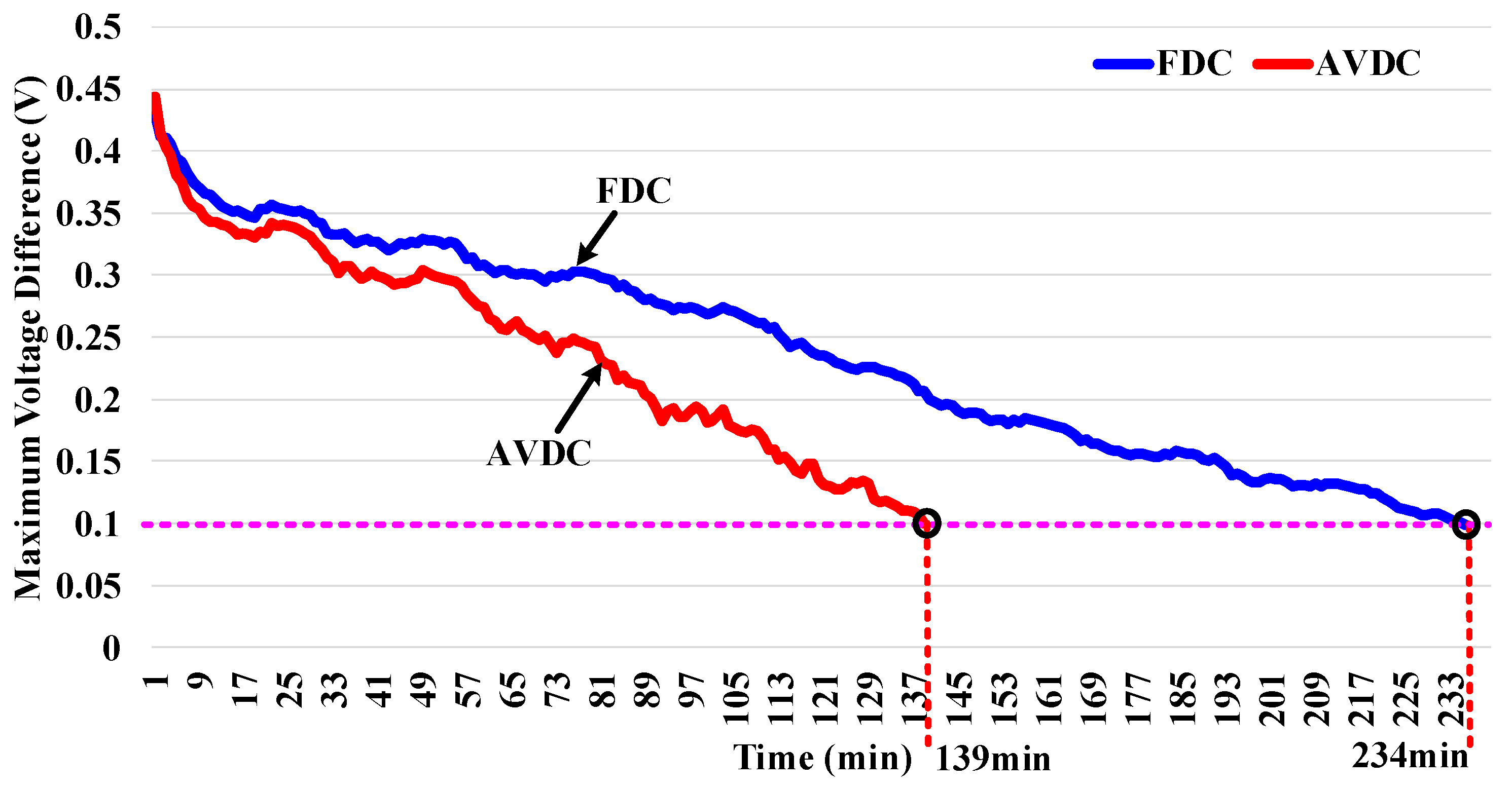
| FDC | 0.43 V | 142% | 234 min | 118% | 83.1% | |
| AVDC | 0.44 V | 139% | 139 min | 127% | 91.4% | |
Publisher’s Note: MDPI stays neutral with regard to jurisdictional claims in published maps and institutional affiliations. |
© 2020 by the authors. Licensee MDPI, Basel, Switzerland. This article is an open access article distributed under the terms and conditions of the Creative Commons Attribution (CC BY) license (http://creativecommons.org/licenses/by/4.0/).
Share and Cite
Wang, S.-C.; Liu, C.-Y.; Liu, Y.-H. A Non-Dissipative Equalizer with Fast Energy Transfer Based on Adaptive Balancing Current Control. Electronics 2020, 9, 1990. https://doi.org/10.3390/electronics9121990
Wang S-C, Liu C-Y, Liu Y-H. A Non-Dissipative Equalizer with Fast Energy Transfer Based on Adaptive Balancing Current Control. Electronics. 2020; 9(12):1990. https://doi.org/10.3390/electronics9121990
Chicago/Turabian StyleWang, Shun-Chung, Chun-Yu Liu, and Yi-Hua Liu. 2020. "A Non-Dissipative Equalizer with Fast Energy Transfer Based on Adaptive Balancing Current Control" Electronics 9, no. 12: 1990. https://doi.org/10.3390/electronics9121990
APA StyleWang, S.-C., Liu, C.-Y., & Liu, Y.-H. (2020). A Non-Dissipative Equalizer with Fast Energy Transfer Based on Adaptive Balancing Current Control. Electronics, 9(12), 1990. https://doi.org/10.3390/electronics9121990