Article

A Novel Bidirectional DC-DC Converter for Dynamic Performance Enhancement of Hybrid AC/DC Microgrid

by
Morteza Daviran Keshavarzi
and
Mohd Hasan Ali
*
Department of Electrical and Computer Engineering, University of Memphis, Memphis, TN 38152, USA
*
Author to whom correspondence should be addressed.
Electronics 2020, 9(10), 1653; https://doi.org/10.3390/electronics9101653
Submission received: 16 September 2020 / Revised: 2 October 2020 / Accepted: 4 October 2020 / Published: 11 October 2020
(This article belongs to the Section Industrial Electronics)

Abstract

:
The conventional bidirectional DC-DC converter (BDC), which employs a half-bridge configuration, has some major disadvantages, including a controller designed for one direction with poor performance in the other direction, a bidirectional operation which does not have symmetrical voltage gain resulting in asymmetrical operation, and step-up and step-down switches that are simultaneously modulated, thereby increasing switching losses. To overcome these drawbacks, this paper proposes a new, nonisolated, DC-DC converter for the bidirectional power flow of battery energy storage applications in DC and hybrid microgrids (HMGs). The proposed converter uses two back-to-back Boost converters with two battery voltage levels, which eliminates step-down operation to obtain symmetric gains and dynamics in both directions. In discharge mode, two battery sections are in parallel connection at a voltage level lower than the grid voltage. In charge mode, two battery sections are in series connection at a voltage level higher than the grid voltage. Simulations demonstrate the efficacy of the proposed converter in the MATALB\Simulink environment. The results show that the proposed converter has promising performance compared to that of the conventional type. Moreover, the novel converter adds no complexity to the control system and does not incur considerable power loss or capital cost.

1. Introduction

The popularity of DC microgrids and their operation along with AC microgrids is increasing due to the elevated level of DC power renewable generations and ubiquitous DC loads. Hybrid microgrids (HMGs) are evolving from the concept stage to real-world practice, as they combine the functionalities of both AC and DC load/generation systems into a synthetic power distribution system. HMGs can reduce power losses due to eliminated frequent conversions from AC to DC and vice versa [1,2,3].
HMGs, particularly in islanded operation, are prone to instability and power fluctuations due to the intermittent nature of renewable energy sources (RES) and the stochastic behavior of the loads. It is imperative to regulate system oscillations with faster dynamics and reliable controllers. Converter-interfaced battery energy storage systems (BESS) [4] are well demonstrated to be the most reliable, technically suitable, and economically available solutions to manage voltage/frequency deviations and to enhance the dynamic performance of microgrids [5].
In an HMG, the DC side BESS is connected to the grid through a bidirectional DC-DC converter (BDC) to control grid voltage or power. The converter is driven to exchange energy between the battery bank and grid to control grid voltage or power mismatches due to power under/oversupply. The conventional BDC frequently used in the literature for energy storage applications [6,7,8,9,10,11,12] is composed of a half-bridge converter and works as a separate Buck converter in step-down mode and Boost converter in step-up mode, with two controllable semiconductor switches. Figure 1 shows the conventional, nonisolated BDC with some drawbacks, as noted below.
(i)
Usually, one controller is used to control the converter in both modes, whereas two converters (Buck and Boost) exhibit two distinctive characteristics that cannot be controlled with one controller, since the controller usually designed based on one converter structure to operate in one mode cannot properly handle grid voltage and load disturbances in both modes.
(ii)
The bidirectional operation does not have symmetrical voltage gain. This asymmetry originates from the different circuit structures in both modes. Therefore, the converter should work with different duty ratios in both modes, resulting in an asymmetric and relatively slow control response during power flow direction changeover. This issue is addressed to some extent by selecting a small enough battery voltage compared to the grid voltage, resulting in a high voltage difference between two sides; otherwise, the Buck operation would not be as effective. However, this potential difference results in high current peaks in both switching operations, leading to high current ripples, particularly in heavy load levels. This issue is usually tackled by selecting a large inductor, thereby incurring a higher capital cost.
(iii)
Both step-up and step-down switches are simultaneously modulated in both modes, resulting in increased converter switching losses that restrict the converter to low power density levels.
Other issues regarding conventional BDC are reported in the literature [13,14] from different viewpoints, although this paper does not aim to address them. Previous studies proposed several isolated and nonisolated bidirectional topologies to improve dynamic performance, gain, efficiency, and operability of BDCs for energy storage and renewable applications.
Resonant converters were of interest in some previous research as they provide the possibility of zero-current/voltage soft-switching operation. Nonisolated, resonant-type, bidirectional converters were proposed to increase the overall voltage gain using coupled inductors and clamping capacitor circuits operating in zero-voltage-switching (ZVS) conditions [15,16]. An isolated, three-port, inductor-capacitor-inductor (LCL)-resonant converter operating in zero-current-switching (ZCS) condition was also implemented in [17] with the capability of integrating photovoltaic (PV) source to energy storage. However, these resonant converters add complexity and cost to both power and control stages and incur more loss due to additional circuit components. In addition, no control strategies were presented that symmetrically worked for both modes in bidirectional applications.
A relatively high voltage gain was achieved for step-down operation using a switched-capacitor cell augmented to a conventional half-bridge [18]. However, this configuration was an improved version of the half-bridge converter, making only a slight improvement only in voltage gain at the cost of additional components with a control design working asymmetrically for both modes. The nonisolated converter in [13] and its improved high-efficiency topology in [19] provided soft-switching operation, employing a 1:1 ideal transformer and pulse-frequency modulation to accommodate load variation and reduced switching loss and to achieve high efficiency. The implemented digital controller used a single loop Proportional-Integral (PI) controller that worked for both modes, with applications in residential energy storage systems.
Research work in [20] proposed a nonisolated BDC employing two conventional Boost converters to achieve the squared value of voltage gain of that of the conventional BDC. Although functional improvements in voltage gain, switching operation, and converter efficiency were obtained in the mentioned literature, the problem of bidirectional asymmetry in voltage gain and control scheme persists. Furthermore, no validating evaluations were conducted for bidirectional applications under the load/generation uncertainties and DC bus voltage variations.
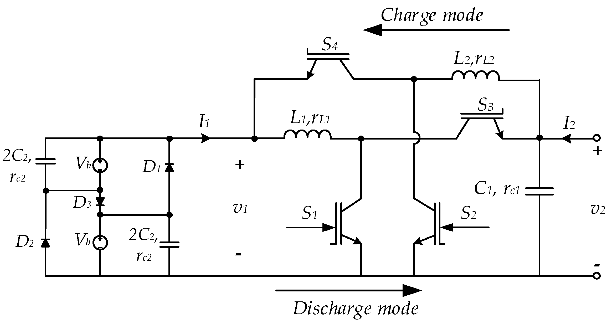
Based on the background research, to overcome the drawbacks of the conventional DC-DC converter this paper proposes a novel bidirectional DC-DC converter for BESS applications in hybrid and DC microgrids (see Figure 2). Several noteworthy features of the proposed converter are as follows:
(i)
It employs two Boost converters in back-to-back topology and has a minimum additional component compared with other proposed converter configurations.
(ii)
Compared to the conventional type, the proposed converter has three more diodes and one more inductor and capacitor. Since there is no Buck operation and the battery voltage can be raised to higher levels, the converter inductors have less inductance and current capacity due to the reduced battery current.
(iii)
The proposed configuration has two voltage levels in the battery side in two modes of operation. The converter exhibits similar dynamic characteristics in both modes of operation, hence, one single controller can be designed and implemented.
Table 1 presents a summarized comparison of the salient features of the proposed BDC in this paper and other BDCs submitted in previously discussed research works. The proposed converter is suitable for voltage and power control in DC microgrids or DC subgrids of HMGs, specifically for high-voltage/high-power applications. The proposed BDC is employed in HMG, as shown in Figure 3, and its efficacy is evaluated by the time-domain simulations presented in Section 4. The HMG in Figure 3 comprises of AC and DC subgrids interconnected through an interlinking converter (ILC) and two distributed energy resources (DERs), as well as a BESS in a DC subgrid. More details are given in Section 4.

2. Proposed DC-DC Converter for BESS System

2.1. Principle of Operation

The proposed converter is composed of two Boost converters in a back-to-back configuration. Therefore, there is only step-up mode in both directions. The objective is to make a bidirectional converter that:
  • Works symmetrically with the same dynamic properties in both directions;
  • Has equally high DC gain in both discharge and charge modes;
  • Does not have much power loss compared with the conventional type;
  • Has a robust yet straightforward controller that fits both modes.
The proposed configuration has two battery voltage levels in two modes of operation, i.e., in discharge mode v 1 < v 2 and in charge mode v 1 > v 2 , as shown in Figure 2. This is made by employing two battery sections with equal voltage levels, which work in parallel in discharge mode and in series in charge mode. Although two battery levels are used, in practice, battery packs are made up of several cells connected in series and parallel to achieve the desired voltage and current. Hence, this would not be a limitation. S 1   and S 2 are modulating switches that are separately controlled by the pulse width modulator (PWM) driver in discharge and charge mode, respectively.
Equal parameters make the base case for two modes. However, the different input/output operational voltages and the converter external network result in different converter dynamics during bidirectional operation. Thus, some adjustments in the power stage and control loops are needed to make a symmetrical bidirectional operation. In this study, it is assumed that r L 1 = r L 2 = r L and r c 1 = r c 2 = r c , where r L and r c are equivalent series resistance (ESR) of the inductor and the capacitor. ON-state resistance ( r o n ) of power switches and diodes are neglected in the theoretical analysis for simplicity [21,22,23], but are included in the simulation analysis for accuracy.
Discharge mode operation:Figure 4 shows the converter circuit in discharge mode. In this mode, S 1 is modulated to boost v 2 , while S 3 is kept ON and S 4 is kept OFF. D 1 and D 2 are in forward-bias and D 3   is in reverse-bias during Boost operation to configure two battery sections in parallel connection to allow current I 1   to flow from v 1   toward v 2 (see Figure 4a). Consequently, battery sections with parallel capacitors are all in parallel connection and v 1 = V b V d , where V b is the battery voltage in each section and V d is the voltage drop across the diode ( D 1 and D 2 ) in forward-bias (see Figure 4b). Due to the low order of magnitude, V d can be neglected in high-voltage applications, i.e., v 1 V b . However, this should not be the case in low-voltage applications.
Charge mode operation: In charge mode, (see Figure 5), S 2 is modulated to boost v 1 , while S 4 is kept ON and S 3 is kept OFF. D 1 and D 2 are in reverse-bias and D 3   is in forward-bias during Boost operation to configure two battery sections in series connection and to allow current I 2   to flow from v 2   toward v 1 (see Figure 5a). As a result, battery sections with parallel capacitors are in series connection with D 3   in between. If D 3 is moved to the lower part of the series connection such that the same current ( I 1 ) flows through it, the circuit configuration remains the same, hence, v 1 = 2 V b + V d , as shown in Figure 5b. It can be shown that I x = 0   and the symmetrical combination of the two battery sections and parallel capacitors are equivalent to one section in parallel with the equivalent capacitor and its ESR, as shown in the left side of Figure 5b. Also, C 2 can be removed since the battery charge level is high enough to keep v 1 constant.
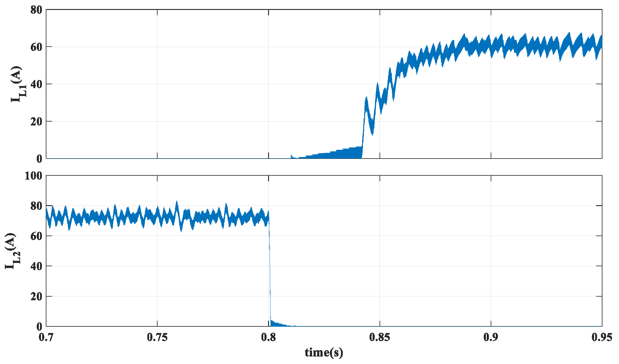
In mode changeover state, inductors are fully discharged before the current flow direction changes. Hence, S 3 and S 4 are switched under zero current conditions. Figure 6 shows a simulation instance of inductor currents and S 3 and S 4 switching conditions during a power flow direction change.
Comparing two modes, the only discrepancy in the converter structure is the value of capacitor ESR equal to 2 r c   in charge mode, which is negligible due to its order of the value. Also, since the values of the capacitor ESR are not proportional to its capacity, the series combination resistance is less than 2 r c . In addition, r c   does not affect the steady-state operation of the converter. It should be noted that since S 3 and S 4 are not continuously modulated, their conduction loss is significantly lower than the switching loss [24]. Also, they should be implemented by devices without body diodes such as insulated-gate bipolar transistors (IGBTs). However, S 1 and S 2 can be implemented by either IGBTs or metal-oxide semiconductor field effect transistors (MOSFETs). Although IGBTs might be suitable for high power/high voltage applications, MOSFETs have lower switching and conduction losses and can work with higher switching frequencies. The maximum stress voltage on all switches is equal to 2 V b and V b for all diodes.
Battery voltage selection: To realize the discharge and charge mode voltage equalization, for a given DC grid rated voltage V d c , such that v 2 = V d c in steady-state, the rated value of battery voltage V b in each section is determined such that the equal steady-state duty ratio is maintained.
{ V d c = V b 1 D                 discharge   mode 2 V b = V d c 1 D                    charge   mode
Then, V b V d c = V d c 2 V b , which yields to
V b = V d c 2

2.2. Converter Transfer Functions

In order to design the converter controllers, a linearized model of the converter is derived based on the state-space averaging for continuous conduction mode (CCM) [21,22]. Since the converter has the same structure (but inequivalent parameter values) in both modes, one equivalent model is derived that is valid for both modes, as depicted in Figure 7.
Averaging takes place over one switching interval T s = 1 / f s , with f s   being the PWM switching frequency with ON- and OFF-state subintervals for S 1 ,   S 2   switches. Averaged, affine continuous-time state-space representation of the converter is given by
{ x ˙ ( t ) = A x ( t ) + B u ( t ) y ( t ) = C x ( t )  
where x ( t ) = [ i L ( t ) v c ( t ) ] T is the state vector, u ( t )   is the converter input voltage e 1 , i L is the inductor current, v c is the capacitor voltage, and y ( t )   is the output. A ,   B , and C are the averaged state transition, input, and output matrices. The converter input voltage ( v 1 in discharge mode and v 2 in charge mode) is assumed to stay constant during Boost operation. With this assumption, i L represents the input current in both modes. Writing the network equations during ON/OFF-state subintervals and establishing state-space equations, we obtain [22]
A = [ 1 L ( r L + d r c R l r c + R l ) d L ( 1 + r c r c + R l ) d R l C ( r c + R l ) 1 C ( r c + R l ) ] B =   [ 1 L 0 ] C = [ d R l ( 1 R l r c + R l ) R l r c + R l ]
where d [ 0 , 1 ] is the duty ratio variable and d = 1 d . R l represents the load resistance estimated based on the converter network discussed hereafter. Averaged value matrices are obtained by combining the corresponding subintervals matrices over one switching period. For the affine system (3) with the initial state x ( 0 ) = x 0 , A is stable and nonsingular, such that x ( t ) converges to equilibrium point X = A 1 B u [25]. Let u = e 1 and y = e 2 , then linearizing (3) results in a two-input, two-output, small-signal model of the converter, represented by the following system of transfer function equations in the s-domain:
[ e 2 ( s ) i L ( s ) ] = [ G 11 G 12 G 21 G 22 ] [ d ( s ) e 1 ( s ) ]
where
G 11 = e 2 ( s ) d ( s )   |   e 1 = 0 = α 0 α 1 s 2 + α 2 s + α 3 α 4 α 5 s 2 + α 4 α 6 s + α 4 2
G 12 = e 2 ( s ) e 1 ( s )   | d = 0 = R l C D r c ( R l + r c ) s + R l D ( R l + r c ) α 5 s 2 + α 6 s + α 4
G 21 = i L ( s ) d ( s )   | e 1 = 0 = α 7 C ( R l + r c ) s + 1 α 4 α 5 s 2 + α 4 α 6 s + α 4 2
G 22 = i L ( s ) e 1 ( s )   | d = 0 = C ( R l + r c ) 2 s + ( R l + r c ) α 5 s 2 + α 6 s + α 4
α 0 = R l E 1 ( R l + r c )   α 1 = L C r c ( R l + r c )    α 2 = C r L r c 2 ( 1 + D ) + [ C R l ( r L D R l D 2 + r L ) C r L D + L ] r c + L R l α 3 = ( R l D + r c + R l D + r c D ) r L R l 2 D 2 α 4 = R l D ( R l D + r c ) + r L ( R l + r c ) α 5 = L C ( R l + r c ) 2   α 6 = [ L + C ( R l r L + r c r L + R l D r c ) ] ( R l + r c ) α 7 = E 1 ( R l + r c ) [ ( 1 r c R l ) r L + r c R L + D R l 2 ]
where D = 1 D is the steady-state value of duty ratio. Expression (5) states that duty ratio d ( s )   and converter input voltage e 1 ( s )   are the independent input controls in the general form. However, the input voltage is assumed here to be approximately constant during Boost operation. Hence, the duty ratio is the only control input. In Equations (6)–(10), E 1 is the DC value of the input voltage e 1   in the steady-state operation. It should be noted that the value of the input voltage is not the same during the two modes.

2.3. Estimation of the Equivalent Load Resistance

Unlike the conventional notion of the unidirectional DC-DC converters, the bidirectional DC-DC converter used in microgrids does not have an explicit load resistance ( R l ) connected to the output terminal. However, the dynamic value of R l   depends on the parameters of the network external to the converter (see Figure 8), which vary during charge and discharge mode operation and are essential parameters for transfer function realization. Conventional methods of calculating transfer functions [21,22,26,27] are based on known values of load resistance. In contrast, in a BDC, the actual value of the load resistance mainly depends on the input/output terminal voltages. This subsection provides a novel yet simple approach to calculating this parameter.
The following network equations hold for the discharge mode (see Figure 8):
{   v 1 = V b R b I 1     v 2 = V d c + R g I 2  
where I 2 = D I 1 and v 1 = D v 2 . In discharge mode, the equivalent load ( R l d c h ) is seen from the v 2 terminal and I 2 flows toward the grid. From (11), we obtain
R l d c h = v 2 I 2 = R g v 2 v 2 V d c   = V b R g D + R b V d c D ( V b D V d c )
It is useful to express the load as a function of the voltage ratio V d c V b to reflect its variation with respect to both battery and DC grid voltage variations. Dividing the nominator and denominator of (12) by V b , we obtain
R l d c h = R g D + R b M D ( 1 D M )
where M = V d c V b . It should be noted, according to (2), M = 2 for the nominal values of V d c and V b In recent equations, R b and R g are the total battery side and grid side resistances, respectively. Similarly, the following network equations satisfy the charge mode:
{ v 1 = 2 V b + 2 R b I 1     v 2 =   V d c R g I 2      
where I 1 = D I 2 and v 2 = D v 1 . In charge mode, the equivalent load resistance ( R l c h ) is seen from the v 1 terminal and I 1 flows toward the battery. From (14), we obtain
R l c h = v 1 I 1 = 2 R b v 1 v 1 2 V b = 2 R b D V d c + 4 R g V b D ( V d c 2 D V b )
Expressed as a function of voltage ratio, (15) becomes
R l c h = 2 R b D M + 4 R g D ( M 2 D )
The superscripts ch and dch refer to charge mode and discharge mode parameter, respectively. The maximum loading (corresponding to the minimum load resistance) occurs for the maximum grid voltage V d c m a x and minimum battery voltage V b m i n   in charge mode and the minimum grid voltage V d c m i n and maximum battery voltage V b m a x   in discharge mode. Figure 9 shows a profile of equivalent load resistance vs. variation of voltage ratio for the test case presented in Table 2. The power stage parameters of the converter can be designed based on conventional ripple-based [26] or optimization-based [28] methods.

2.4. Power Stage Adjustment

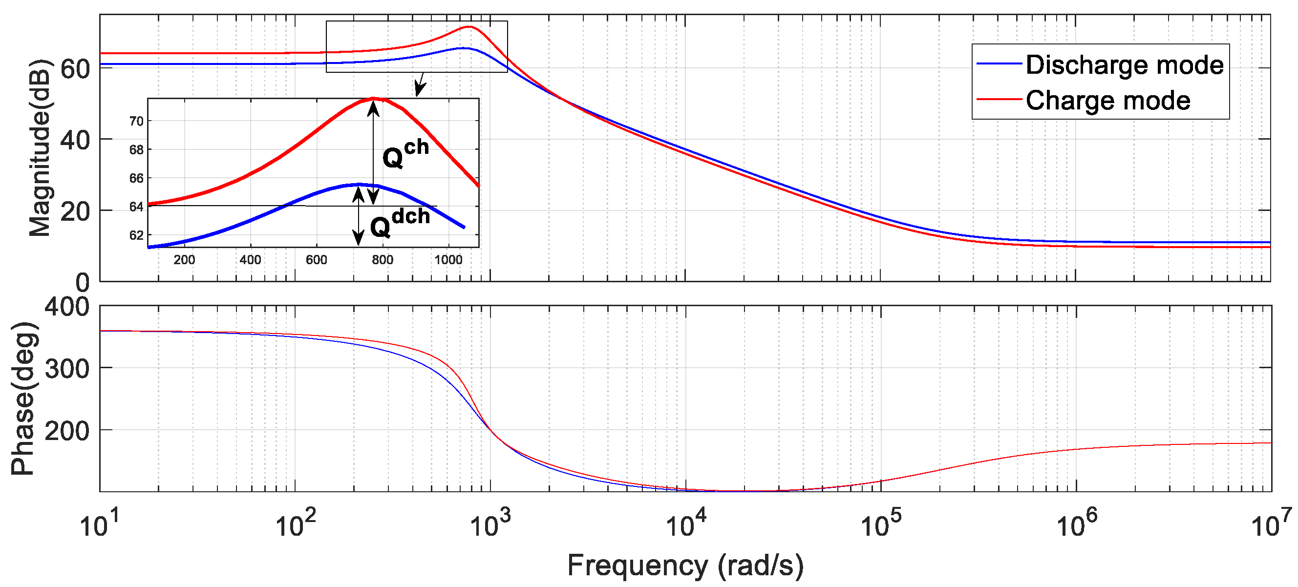
Although the equal values of the inductor and capacitor for charge and discharge mode Boost converters theoretically result in similar dynamics, the external network causes unequal loading for each mode, resulting in small discrepancies that deteriorate the dynamic performance when working as a bidirectional converter. Therefore, an adjustment in the internal configuration is needed to tackle this discrepancy. Figure 10 shows the bode plot of the open-loop transfer function of the unadjusted Boost converters in both modes of operation for G 11 ( s ) for the converter parameters shown in Table 2. There are two significant differences between the two modes, i.e., the quality factor and high/low-frequency gains. This section deals with the former to provide equal dynamic performance. The latter is discussed in the next section.
From the characteristic equation of the system given in (6) and (8) and comparing with the standard form of a second-order system’s equation [26,27], the quality factor Q   and corresponding resonant frequency ω r are defined as
Q = : 1 α 6 α 4 α 5      ω r = : α 4 α 5
The quality factor in frequency response corresponds to time-domain overshoot and is correlated to the damping ratio δ , as in Q = 1 2 δ . In general, with the symmetrical form of the proposed bidirectional converter, the discharge mode has a smaller quality factor due to the higher loading and can be chosen as the reference. Hence, equating the quality factor in discharge mode with that of the value in the charge mode yields the adjusted L 2 and C 2 .
( 1 α 6 α 4 α 5 ) c h = Q d c h
In addition, to maintain the same resonant frequency, we use
( α 4 α 5   ) c h = ω r d c h
Substituting coefficients (10) into (17) for the charge mode using the rated values of load resistance R l c h and input voltage E 1 c h in (18) and (19) yields
Q d c h 2 L 2 2 + Q d c h 2   γ 2 C 2 2 + ( Q d c h 2 γ α 4 ) α 4 L 2 C 2 = 0 ω r d c h 2 ( R l c h + r c ) 2 L 2 C 2 α 4 = 0 γ = R l c h r L + r c r L + R l c h D r c
subject to
L 2 m i n < L 2 < L 2 m a x   and   C 2 m i n < C 2 < C 2 m a x
where (20) is a bivariate quadratic system of equations that can be solved for L 2 and C 2 . The minimum values of the inductor and the capacitor are obtained based on ripple criteria. An estimation of the maximum values can be roughly calculated based on the ratio of load resistances, such that L 2 m a x / L 1 R l c h / R l d c h and C 1 / C 2 m a x R l c h / R l d c h . Figure 11 shows the bode plot of the adjusted converter with equal quality factors for the converter’s case, as presented in Table 2.

3. Control System

The transfer functions derived in the earlier sections can be utilized to design different schemes of closed-loop controllers based on the linearized models. The BESS in the DC grid is usually used in the grid-forming operation to control DC grid voltage. In contrast, in grid-following operation, power is injected/absorbed to track the reference power signals defined by the power management system (PMS). The power mode control is designed based on the current controller using a reference power to generate the reference current. Here, a design approach is presented based on the frequency response of open/closed-loop gain transfer function for the proposed BDC controller design presented in Section 3.1. Section 3.2 briefly discusses the conventional BDC controller scheme as a background framework for the comparison made in Section 4.

3.1. Proposed Converter Controller

3.1.1. Current Control Mode

Figure 12a illustrates a block diagram of the small-signal model of the converter with the current controller. G c i , K P W M , and H c are the compensator, the PWM gain, and the feedback sensor’s transfer function, respectively.
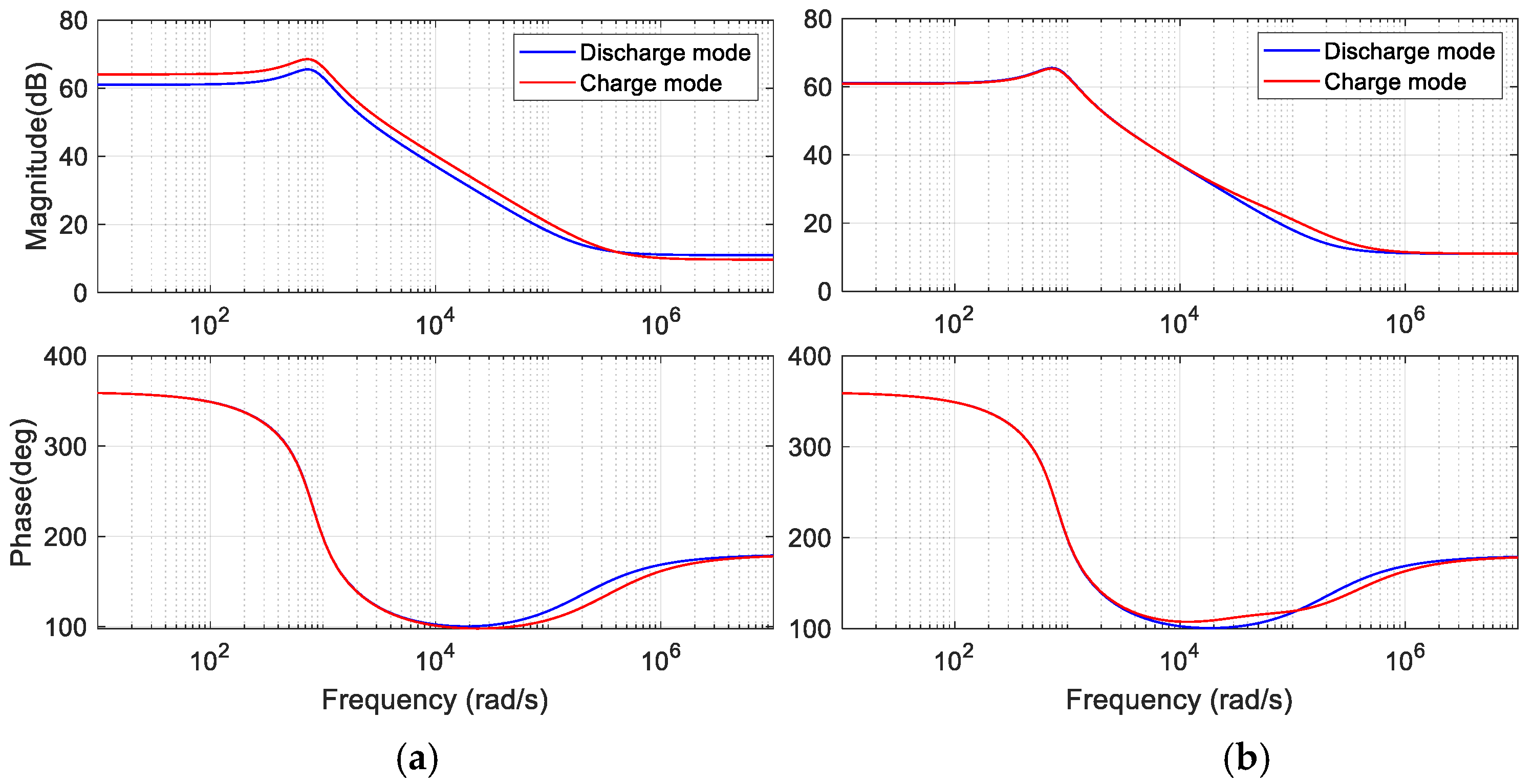
Figure 13a shows the bode plot of the open-loop G 21 for both modes with adjustment made in the power stage for the case study presented in Table 1, which has a similar phase but dissimilar gain. Before the controller is designed, another adjustment is needed to obtain equal bidirectional gain dynamics.
The overall behavior of G 21 is similar to a single real pole, which is G 21 0 s ω b 21 + 1 , where ω b 21 is the cut-off frequency and G 21 0 = α 7 α 4 2 is the DC gain. By neglecting ESRs, G 21 0 2 E 1 R l D 3 is obtained in terms of converter rated values for the Boost converter, as depicted in Figure 6. In the low frequency, | G 21 ( s ) | = G 21 0 , whereas in the high frequency, the gain decreases with a slope of −20 dB/dec. The adjustment made in the earlier section guarantees equal bidirectional bandwidth for G 21 . Therefore, to have the same bidirectional gain crossover frequency, the following equity should be supported:
G 21 0 c h = G 21 0 d c h 2 V d c R l c h D ' 3 = 2 V b R l d c h D ' 3
Selecting the discharge mode as reference, gain coefficient K I is obtained from (21) for the charge mode current control loop.
K I = V b R l c h V d c R l d c h
Figure 13b shows the bode plot of both modes for the open-loop G 21  after applying gain adjustment, yielding analogous bidirectional dynamics. The closed-loop current controller can be designed based on the discharge mode parameters, which is the reference mode. For sufficient disturbance rejection during load variation, we choose the lag type controller for G c i . Although the lag controller relatively reduces converter response (hence its bandwidth), it reduces the switching noise in the feedback signal. Inspired by the method discussed in [26], the compensator transfer function is given by
G c i ( s ) = k p i ( 1 + ω c i s )
where k p is the proportional gain and ω c i is the controller’s zero, which is selected at least one decade below the closed-loop gain crossover frequency ω c 21 to maintain an adequate phase margin and therefore system stability. On the other hand, to suppress switching harmonics, ω c 21 is placed well below the switching frequency f s . The approximate practical proportions ω c 21 = 2 π f s 4 and ω c i = ω c 21 10   are chosen for this work. The unity value of the loop gain of the compensated current control loop occurs at ω c 21 , i.e., | L ( j ω c 21 ) | = K P W M | G c i ( j ω c 21 ) G 21 ( ω c 21 ) H c ( j ω c 21 ) | = 1 . The value of the controller gain is | G c i | = 1.1 k p i at this frequency. Then, the compensator’s coefficient is obtained as follows:
k p i = 1 1.1 K P W M | G 21 ( j ω 21 ) H ( j ω 21 ) |
Since the approach is practical, further tuning might be needed to ensure closed-loop stability, limited overshoot, and reasonable phase margin. The reference current I r e f is calculated based on the reference power P r e f acquired from PMS. In the current (power) control mode, it is assumed that other devices in the grid control the grid voltage. The sign of P r e f determines the converter operation mode as follows:
{ P r e f > 0 ,   I r e f = P r e f v 2 C h a r g e   m o d e P r e f < 0 ,   I r e f = P r e f D η v 2 D i s c h a r g e   m o d e
where η is the converter efficiency in discharge mode and can be calculated for a Boost converter; if ESRs are neglected, η = 1 . P r e f is a reference signal obtained from PMS to compensate for real-time load/generation power mismatch or constant charging.

3.1.2. Voltage Control Mode

As Figure 11 shows, due to the asymmetric property of the converter in two modes, the high- and low-frequency gain values are not the same for the open-loop duty ratio-to-output voltage G 11 ( s ) . Gain equalization further results in bidirectional dynamic symmetry. For the voltage control loop with discharge mode being the target frequency response, the following equations hold:
lim ω 0 | G 11 d c h ( j ω ) | lim ω 0 | G v ( j ω ) . G 11 c h ( j ω ) | lim ω | G 11 d c h ( j ω ) | lim ω | G v ( j ω ) . G 11 c h ( j ω ) |
where G v ( s ) should be a filter with negligible change in phase to match the asymptotic low- and high-frequency gains of charge mode to that of discharge mode. We consider a pair of real pole/zero, given by
G v ( s ) = K v s + ω z s + ω p
where K v , ω z and ω p are the filter’s high-frequency gain, zero, and pole, respectively, and should be designed to match bidirectional dynamics for G 11 . The filter should reduce low-frequency gain and raise high-frequency gain while causing an insignificant change in phase to obtain the target frequency response. For a Boost converter, neglecting ESRs results in | G 11 | = E 1 R l D C as ω and | G 11 | = E 1 D 2 as ω 0 . Therefore, the criteria outlined in (26) determine the following asymptotes:
K v = lim ω | G 11 d c h ( j ω ) | | G 11 c h ( j ω ) | = V b R l c h C 2 V d c R l d c h C 1 K v ω z ω p = lim ω 0 | G 11 d c h ( j ω ) | | G 11 c h ( j ω ) | = V d c V b ω z ω p = V d c 2 R l d c h C 1 V b 2 R l c h C 2
This means the filter gain rolls off from a nonzero DC gain in ω z and rolls on to a nonzero asymptotic gain in ω p , with a slope of K v ω p ω z 2   ω p > 0 , ω z < ω p . The maximum phase angle of ϕ m = tan 1 ( ω p ω z 2 ω p ω z )   occurs at the frequency of ω m = ω p ω z . Proper choice of ω z (and ω p ) results in a suitable gain fit and insignificant phase angle discrepancy between two modes. Since the adjustment made in the power stage in the previous section guarantees the same bidirectional cut-off frequency, a good approximation is to equate the zero with the cut-off frequency of G 11 ( s ) , i.e., ω z = ω c 11 . Figure 14 compares the bode plots of the power stage-adjusted transfer function G 11 ( s )   for gain compensated and uncompensated charge mode for the case study presented in Table 2. In this example, a maximum of ϕ m = 14.8 ° occurs in the phase angle at ω m = 46.64   krad / s , which negligibly changes the charge mode gain and phase in this vicinity but makes an overall frequency response fit with reference to the discharge mode.
Figure 15a shows the small-signal model of the converter based on the linearized model for the voltage controller based on the discharge mode parameters. In the voltage control mode, the objective is to control the grid voltage by tracking the reference value V r e f which is given by
V r e f = V * + R g I ¯ 2     I ¯ 2 = ω f i s + ω f i I 2
where V * is the voltage set point of the converter at the connection terminal v 2 that, in general, is equal to V d c , and ω f i is the cut-off frequency of a low-pass filter to suppress converter current-switching harmonics. The following transfer function is given for the voltage compensator, a lag type controller analogous to that of the current controller counterpart:
G c v ( s ) = K p v ( 1 + ω c v s )
where K p v and ω c v are the controller’s proportional gain and zero obtained in an analogous way to that of the current controller in the previous section. It should be noted that the voltage controller must be much slower than the current controller, resulting in a lower bandwidth since, as observed in Figure 14, G 11 has one pole which is not rejected at high frequency. On the other hand, this single loop voltage control is relatively faster than the conventional design dual-loop scheme in response to grid voltage variations. As the DC grid voltage gets stiffer, the dynamics of the BDC in voltage control mode tend to be more oscillatory, particularly under heavy loads. This property of BDC makes it disparate from the unidirectional converter, where the steady-state duty ratio D varies based on the load value. In a bidirectional converter, D is a constant defined by the grid and battery voltages given in (1) and (2). Note that the battery voltage does not change significantly across the operational range of state of charge (SoC). Figure 16 shows the battery voltage variation for the typical minimum and maximum ranges of SoC under four loading conditions. Therefore, there should be a maximum limit for the inductor value to restrict the magnitude of the voltage oscillations in v 2 during heavy loading. This situation results in a tradeoff between inductor current ripples and voltage oscillations in the full load.

3.2. Conventional BDC Controller

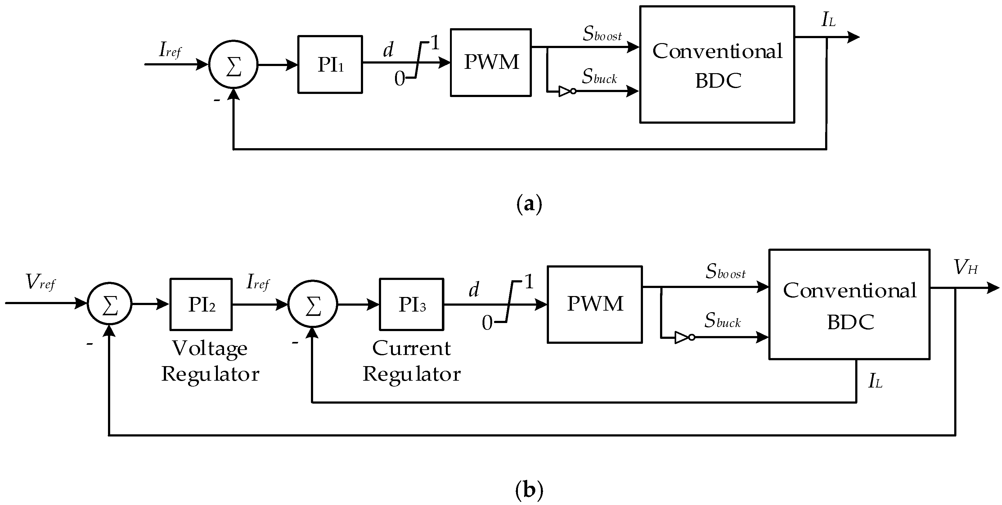
The power stage diagram in Figure 1 is used for the conventional BDC, with the parameters equal to the discharge mode of the proposed BDC. The control system of the conventional BDC is a single loop PI controller [18,29] for the current control mode displayed in Figure 17a, and a dual-loop PI-based control [10] for the voltage control mode illustrated in Figure 17b. Table 3 presents all the parameters of conventional BDC. The variables k p and k i in Table 3 refer to the proportional and integral gains, respectively, of the PI controllers illustrated in Figure 17.

4. Simulation Results

In this section, the effectiveness of the proposed converter is evaluated and compared with that of the conventional type for the converter case presented in Table 2. The case study HMG includes a three-phase 460 V/60 Hz AC grid and an 800 V DC grid power system, as shown in Figure 3, with the parameters presented in Table 4. It is simulated using detailed switching models for power electronic devices by applying a sampling frequency of 2 MHz for discrete time-domain simulations performed in the MATLAB\Simulink environment. In total, three instances are simulated using the test systems for two separate cases, as detailed below.
  • Case I—Grid-connected HMG: In this state, the DC grid is connected to the main grid through a grid-following interlinking converter (ILC). In the voltage control mode, the BDC controls the DC grid voltage, while ILC tracks the reference powers. In the current control mode, this scheme switches between BDC and ILC.
  • Case II—Islanded HMG: In this state, Case I is modified to form an islanded HMG. In the voltage control mode of BDC, the ILC is a grid-forming voltage source converter (VSC), and DER1 is a grid-following generation source to supply reference active/reactive powers. All control systems of VSCs in ILC and DER1 are well-established structures adopted from [30].
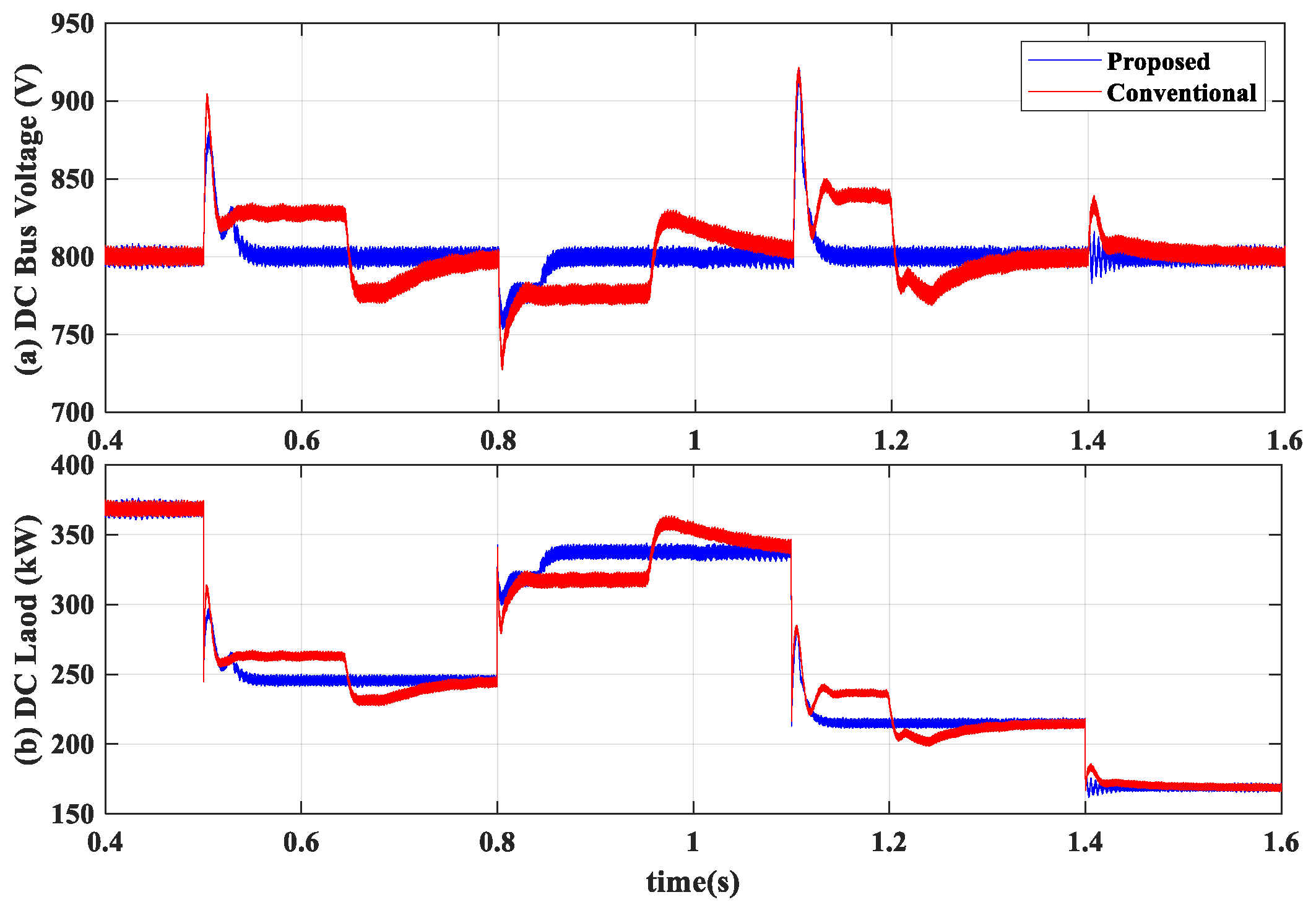
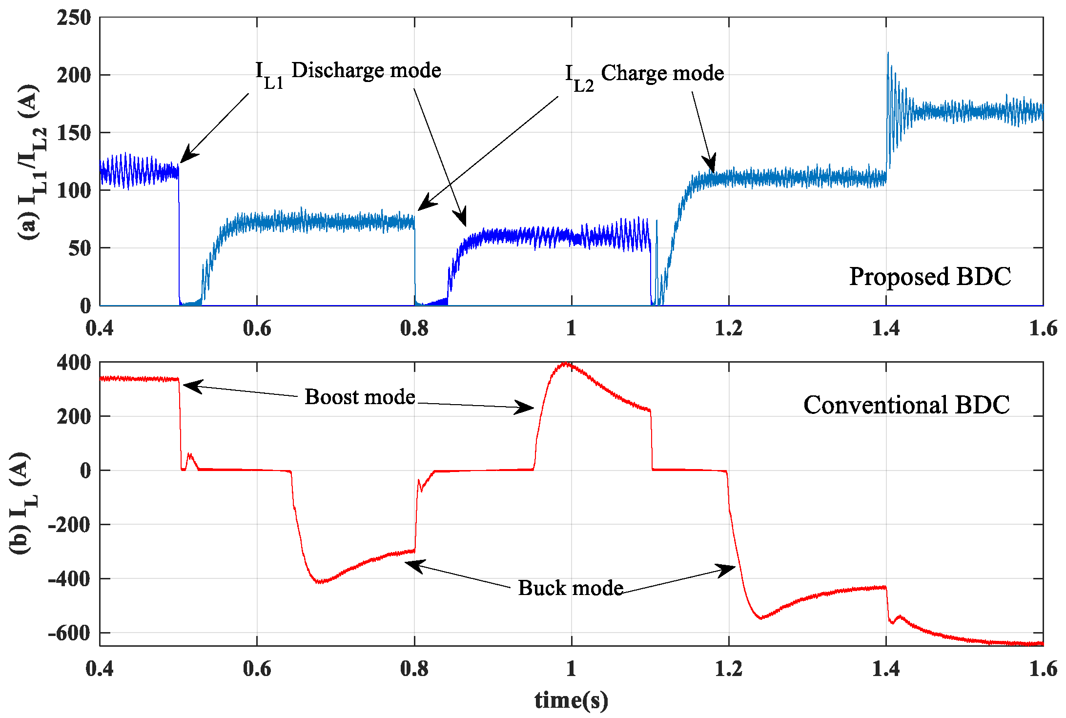
A narrow-band dead zone is implemented in both converters’ control systems to prevent discontinuous conduction mode (DCM) operation. An equal value of ON-state resistance ( r o n = 5   m Ω ) is considered for all power switches and diodes in both converter types. DER2 is modeled as a solar PV connected via a DC-DC converter to DC bus to track the maximum power point. Figure 18, Figure 19 and Figure 20 show the dynamic response of the system to the separate pulsed changes in DC load in Case I for current and voltage control modes, respectively. At first, the DC load demands 370 kW power. For the voltage control mode, starting from 0.5 s, four subsequent step changes occur, i.e., [170 216 244 334] kW, in 0.3 s intervals. For the current control mode, three subsequent pulsed variations take place, i.e., [257 130 590] kW, in 0.5 s intervals. In the current control mode, the controller effort is lighter than that of the voltage control mode, despite the heavier load change. The significant performance of the proposed BDC can be observed in mode changeovers from discharge to charge mode and vice versa. Although the conventional BDC works well in Boost operation, it has deficient performance during Buck mode.
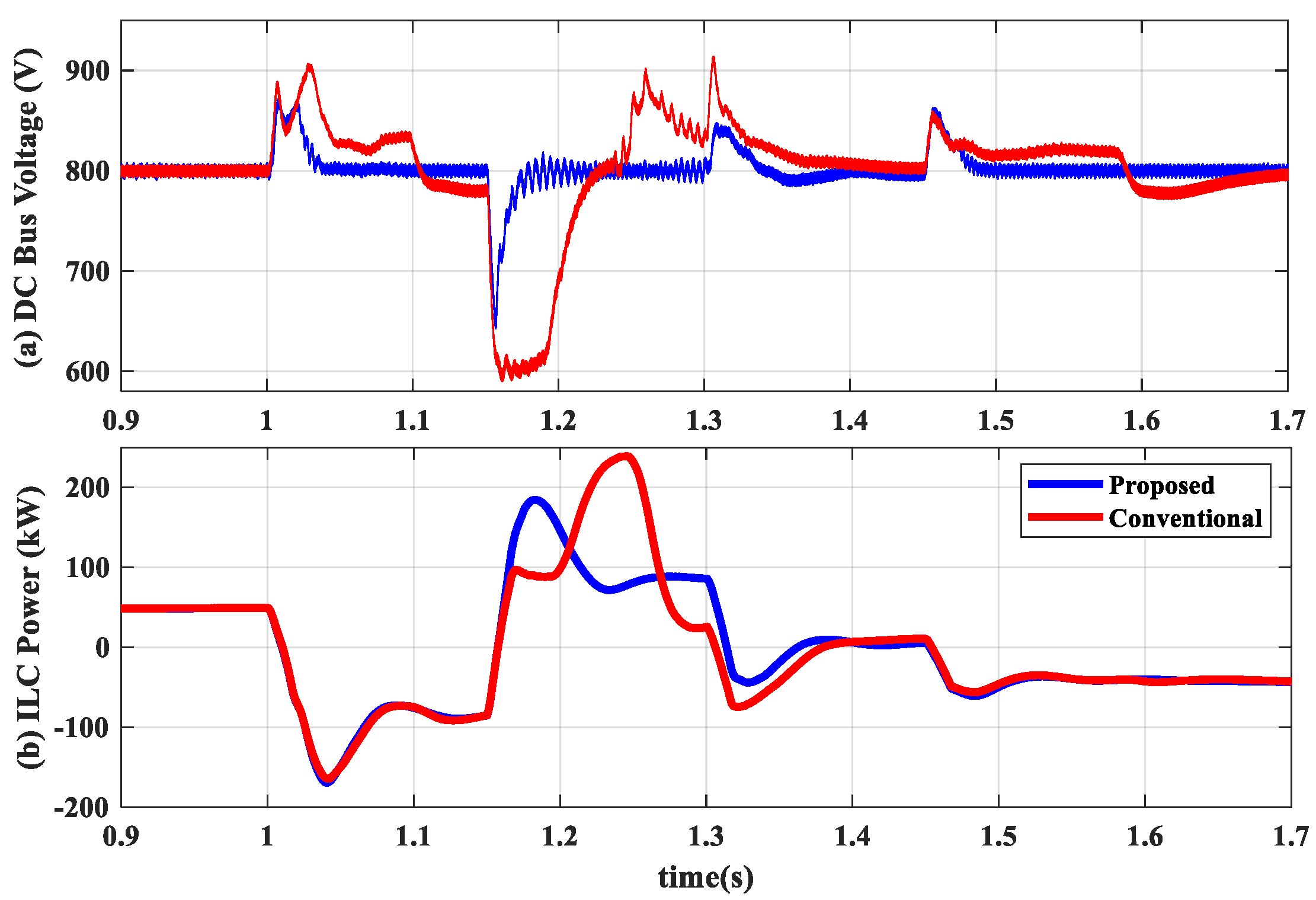
Figure 21 illustrates the system’s dynamic response to the active power generation variations in DER1 for Case II with BDC in the voltage control mode. Initially, DER1 generates 150 kW of active power, causing ILC to exchange 50 kW power from the DC side to the AC side. Starting from second 1, four subsequent power generation disturbances, i.e., [100 200 250 300] kW, occur in 150 ms intervals in DER1. This power fluctuation in the AC side propagates to the DC side by exchanging power in ILC, as shown in Figure 21. Like Case I, the mode changeover performance in the proposed BDC is superior to that of the conventional type, resulting in a faster response to grid voltage variations.

5. Conclusions

This study proposed a novel bidirectional DC-DC converter for energy storage applications in DC microgrid and HMG systems composed of two back-to-back Boost converters in the power stage adjusted to symmetrical operation, as well as an equal gain ratio in both charge and discharge modes. Systematical methodologies were implemented based on the frequency response of converter plant models in charge and discharge modes. A novel approach was proposed to estimate the equivalent load resistance for each operation mode, which is a key parameter in open-loop transfer functions rendering the converter loading to not be equal during two modes. The efficacy of the proposed converter was evaluated and compared with that of the conventional type via two case studies for voltage and current mode controllers, respectively. The simulation results demonstrated that the proposed converter exhibited superior performance in handling power and voltage fluctuation in the DC grid. The battery voltage (low-voltage side) must be selected in proportion to DC bus voltage (high-voltage side), representing the only limitation of this converter.
In future research, the effectiveness of the proposed BDC should be evaluated in more realistic HMGs, including diverse generation sources like wind turbine generators and diesel generators employing advanced controllers. Finally, as a necessary complement to this study, the experimental verification of the proposed DC-DC converter should be performed in future research.

Author Contributions

Conceptualization, M.D.K.; Formal analysis, M.D.K.; Methodology, M.D.K.; Project administration, M.H.A.; Resources, M.H.A.; Supervision, M.H.A.; Writing–review & editing, M.D.K. and M.H.A. All authors have read and agreed to the published version of the manuscript.

Funding

This research received no external funding.

Conflicts of Interest

The authors declare no conflict of interest.

References

  1. Kirakosyan, A.; El-Saadany, E.F.; El Moursi, M.S.; Yazdavar, A.H.; Al-Durra, A. Communication-Free Current Sharing Control Strategy for DC Microgrids and Its Application for AC/DC Hybrid Microgrids. IEEE Trans. Power Syst. 2020, 35, 140–151. [Google Scholar] [CrossRef]
  2. Daviran Keshavarzi, M.; Ali, M.H. FRT Capability Enhancement of Autonomous AC/DC Hybrid Microgrid by Coordinated MSDBR and Interlinking Converter Control Strategy. In Proceedings of the IEEE Power & Energy Society Innovative Smart Grid Technologies Conference (ISGT), Washington, DC, USA, 18–21 February 2019; pp. 1–5. [Google Scholar]
  3. Eisapour-Moarref, A.; Kalantar, M.; Esmaili, M. Power Sharing in Hybrid Microgrids Using a Harmonic-Based Multi-Dimensional Droop. IEEE Trans. Ind. Inform. 2020, 16, 109–119. [Google Scholar] [CrossRef]
  4. Daviran Keshavarzi, M.; Ali, M.H. Disturbance Resilience Enhancement of Islanded Hybrid Microgrid Under High Penetration of Renewable Energy Resources by BESS. In Proceedings of the IEEE Transmission & Distribution, Chicago, IL, USA, 12–30 October 2020. [Google Scholar]
  5. Daviran Keshavarzi, M.; Ali, M.H. Influence of Battery Energy Storage Location on the Dynamic Performance of Hybrid AC/DC Microgrid. In Proceedings of the 2nd International Conference on Smart Power & Internet Energy Systems, Bangkok, Thailand, 15–18 September 2020. [Google Scholar]
  6. Corti, M.; Tironi, E.; Ubezio, G. DC networks including multiport DC/DC converters: Fault analysis. IEEE Trans. Ind. Appl. 2016, 52, 3655–3662. [Google Scholar] [CrossRef] [Green Version]
  7. Zhu, X.; Meng, F.; Xie, Z.; Yue, Y. An Inertia and Damping Control Method of DC-DC Converter in DC Microgrid. IEEE Trans. Energy Convers. 2020, 35, 799–807. [Google Scholar] [CrossRef]
  8. Kotra, S.; Mishra, M.K. Design and Stability Analysis of DC Microgrid With Hybrid Energy Storage System. IEEE Trans. Sustain. Energy 2019, 10, 1603–1612. [Google Scholar] [CrossRef]
  9. Khodamoradi, A.; Liu, G.; Mattavelli, P.; Caldognetto, T.; Magnone, P. Analysis of an On-Line Stability Monitoring Approach for DC Microgrid Power Converters. IEEE Trans. Power Electron. 2019, 34, 4794–4806. [Google Scholar] [CrossRef]
  10. Kwon, M.; Choi, S. Control Scheme for Autonomous and Smooth Mode Switching of Bidirectional DC-DC Converters in a DC Microgrid. IEEE Trans. Power Electron. 2018, 33, 7094–7104. [Google Scholar] [CrossRef]
  11. Saleh, M.; Esa, Y.; Mohamed, A. Impact of Communication Latency on the Bus Voltage of Centrally Controlled DC Microgrid during Islanding. IEEE Trans. Sustain. Energy 2018, 10, 1844–1856. [Google Scholar] [CrossRef] [Green Version]
  12. Morstyn, T.; Savkin, A.; Hredzak, B.; Agelidis, V. Multi-Agent Sliding Mode Control for State of Charge Balancing Between Battery Energy Storage Systems Distributed in a DC Microgrid. IEEE Trans. Smart Grid 2018, 9, 4735–4743. [Google Scholar] [CrossRef] [Green Version]
  13. Choi, Y.G.; Lee, S.W.; Lee, H.S.; Lee, S.C.; Kang, B. Increase in Power Conversion Efficiency of Bidirectional DC-DC Converter Using 1:1 Transformer and Pulse-Frequency Modulation Control. IEEE Trans. Power Electron. 2018, 33, 10539–10549. [Google Scholar] [CrossRef]
  14. Lin, C.; Yang, L.; Wu, G.W. Study of a non-isolated bidirectional DC-DC converter. IET Power Electron. 2012, 6, 30–37. [Google Scholar] [CrossRef]
  15. Rathore, A.K.; Patil, D.R.; Srinivasan, D. Non-isolated Bidirectional Soft-Switching Current-Fed LCL Resonant DC/DC Converter to Interface Energy Storage in DC Microgrid. IEEE Trans. Ind. Appl. 2016, 52, 1711–1722. [Google Scholar] [CrossRef]
  16. Aamir, M.; Mekhilef, S.; Kim, H.J. High-Gain Zero-Voltage Switching Bidirectional Converter With a Reduced Number of Switches. IEEE Trans. Circuits Syst. II Express Briefs 2015, 62, 816–820. [Google Scholar] [CrossRef]
  17. Zeng, J.; Qiao, W.; Qu, L. An Isolated Three-Port Bidirectional DC-DC Converter for Photovoltaic Systems With Energy Storage. IEEE Trans. Ind. Appl. 2015, 51, 3493–3503. [Google Scholar] [CrossRef]
  18. Cornea, O.; Andreescu, G.D.; Muntean, N.; Hulea, D. Bidirectional Power Flow Control in a DC Microgrid Through a Switched-Capacitor Cell Hybrid DC-DC Converter. IEEE Trans. Ind. Electron. 2017, 64, 3012–3022. [Google Scholar] [CrossRef]
  19. Ham, S.H.; Choi, Y.G.; Lee, H.S.; Lee, S.W.; Lee, S.C.; Kang, B. High-efficiency bidirectional buck-boost converter for residential energy storage system. Energies 2019, 12, 3786. [Google Scholar] [CrossRef] [Green Version]
  20. Ardi, H.; Ajami, A.; Kardan, F.; Avilagh, S.N. Analysis and Implementation of a Nonisolated Bidirectional DC-DC Converter with High Voltage Gain. IEEE Trans. Ind. Electron. 2016, 63, 4878–4888. [Google Scholar]
  21. Mariéthoz, S.; Almér, S.; Bâja, M.; Beccuti, A.G.; Patino, D.; Wernrud, A.; Buisson, J.; Cormerais, H.; Geyer, T.; Jonsson, U.T.; et al. Comparison of Hybrid Control Techniques for Buck and Boost DC-DC Converters. IEEE Trans. Control Syst. Technol. 2010, 18, 1126–1145. [Google Scholar] [CrossRef]
  22. Ioinovici, A. Power Electronics and Energy Conversion Systems, Fundamentals and Hard-Switching Converters; WILEY: West Sussex, UK, 2013; Volume 1, ISBN 9780470710999. [Google Scholar]
  23. Taheri, A.; Ghasemian, A.; Ren, H. Boost Converters’ Proximate Constrained Time-Optimal Sliding Mode Control Based on Hybrid Switching Model. Complexity 2019, 2019. [Google Scholar] [CrossRef]
  24. Chakraborty, S.; Mazuela, M.; Tran, D.D.; Corea-Araujo, J.A.; Lan, Y.; Loiti, A.A.; Garmier, P.; Aizpuru, I.; Hegazy, O. Scalable Modeling Approach and Robust Hardware-in-the-Loop Testing of an Optimized Interleaved Bidirectional HV DC/DC Converter for Electric Vehicle Drivetrains. IEEE Access 2020, 8, 115515–115536. [Google Scholar] [CrossRef]
  25. Ghasemian, A.; Taheri, A. Constrained Near-Time-Optimal Sliding-Mode Control of Boost Converters Based on Switched Affine Model Analysis. IEEE Trans. Ind. Electron. 2018, 65, 887–897. [Google Scholar] [CrossRef]
  26. Kazimierczuk, M.K. Pulse-Width Modulated DC-DC Power Converters, 2nd ed.; John Wiley & Sons, Ltd.: Chichester, West Sussex, UK, 2015; ISBN 9780470773017. [Google Scholar]
  27. Erickson, R.W.; Maksimović, D. Fundamentals of Power Electronics, 2nd ed.; Kluwer: New York, NY, USA, 2004; ISBN 0-306-48048-4. [Google Scholar]
  28. Veerachary, M.; Saxena, A.R. Optimized power stage design of low source current ripple fourth-order boost DC-DC converter: A PSO approach. IEEE Trans. Ind. Electron. 2015, 62, 1491–1502. [Google Scholar] [CrossRef]
  29. Elserougi, A.; Abdelsalam, I.; Massoud, A.; Ahmed, S. A bidirectional non-isolated hybrid modular DC-DC converter with zero-voltage switching. Electr. Power Syst. Res. 2019, 167, 277–289. [Google Scholar] [CrossRef]
  30. Rocabert, J.; Luna, A.; Blaabjerg, F.; Rodríguez, P. Control of Power Converters in AC Microgrids. IEEE Trans. Power Electron. 2012, 27, 4734–4749. [Google Scholar] [CrossRef]
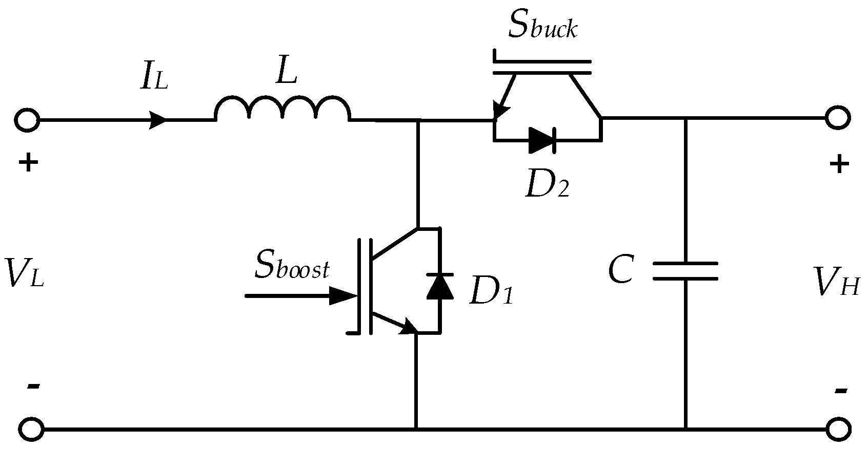
Figure 1. Conventional bidirectional DC-DC converter.
Electronics 09 01653 g001
Figure 2. Proposed bidirectional DC-DC converter.
Electronics 09 01653 g002
Figure 3. Hybrid microgrid under the study.
Electronics 09 01653 g003
Figure 4. Discharge mode circuit. (a) Current flow diagram; (b) equivalent circuit.
Electronics 09 01653 g004
Figure 5. Charge mode circuit. (a) Current flow diagram; (b) equivalent circuit.
Electronics 09 01653 g005
Figure 6. Inductor currents and S 3 S 4   switching conditions during power a flow direction change.
Electronics 09 01653 g006
Figure 7. Equivalent Boost converter circuit; e 1 and e 2 represent input and output voltages, respectively, and R l represents the converter equivalent load in each mode.
Electronics 09 01653 g007
Figure 8. Converter connection network. ( · ) stands for charge mode operating parameters.
Electronics 09 01653 g008
Figure 9. Load resistance variation for the test case presented in Table 2.
Electronics 09 01653 g009
Figure 10. Bode plot of unadjusted converter for open-loop G 11 ( s ) with zoomed-in magnitude.
Electronics 09 01653 g010
Figure 11. Bode plot of the adjusted converter for open-loop G 11 ( s ) .
Electronics 09 01653 g011
Figure 12. Current controller block diagram of the proposed converter. (a) Closed-loop small-signal model based on the discharge mode parameters for reference; (b) plant model.
Electronics 09 01653 g012
Figure 13. Bode plots of duty ratio-to-inductor current G 21 ( s ) . (a) uncompensated charge mode gain; (b) compensated charge mode gain.
Electronics 09 01653 g013
Figure 14. Bode plots of duty ratio-to-output voltage ( v 2 ) ,   G 11 ( s ) .   (a) Uncompensated charge mode; (b) compensated charge mode.
Electronics 09 01653 g014
Figure 15. Voltage controller block diagram of the proposed converter. (a) Closed-loop small-signal model based on the discharge mode parameters as reference; (b) plant model.
Electronics 09 01653 g015
Figure 16. Battery voltage vs. state of charge (SoC) for different loading conditions.
Electronics 09 01653 g016
Figure 17. Conventional BDC control systems used for comparison analysis. (a) Current control; (b) voltage control.
Electronics 09 01653 g017
Figure 18. Converter response to pulsed DC load change for Case I with voltage control mode.
Electronics 09 01653 g018
Figure 19. Inductor currents in voltage control mode for Case I.
Electronics 09 01653 g019
Figure 20. Converter response to pulsed DC load changes for Case I with the current controller.
Electronics 09 01653 g020
Figure 21. System response to power generation variation in DER1 in Case II with BDC in voltage control.
Electronics 09 01653 g021
Table 1. Comparison between proposed, conventional, and other bidirectional DC-DC converters (BDCs).
ProposedConventional [15][18][13]/[19][20][16]
Voltage gain in discharge mode 1 1 D 1 1 D 2 G 1   ( 1 ) 1 D b o o s t 1 + D 1 D 1 1 D ( 1 1 D ) 2 2 + D 1 D
Voltage gain in charge mode 1 1 D D 1 2 D b u c k G 2   ( 1 )   1 D 1 + D D D 2 ( 1 D ) D 2 D 2 + 1
Symmetrical scheme
Control complexitylowlowhighlowmediumlowhigh
Component count:-------
Inductors21323/321
Capacitors (2)00322/212
Switching devices42432/443
Diodes (3)3-----3
Coupled inductors----1/1-1
(1)  G 1 , G 2 are functions of switching frequency, load resistance, and reactance of the resonant circuit parameters. (2) Input/output capacitors are not counted. (3) Body diodes are not considered.
Table 2. Parameters of the proposed BDC.
C 1 500   μ F C 2 300   μ F r c 10   m Ω
L 1 0.45   mH L 2 0.72   mH r L 0.5   m Ω
V b 565   V V d c 800   V ω f i 500   rad / s
R b 11   m Ω R g 25   m Ω f s 50   kHz
k p i , ω c i 0.0003 ,   8340   rad / s k p v , ω c v 0.00199 ,   196   rad / s
K P W M 1 H v 1 H c 1
Battery:Capacity 300   Ah TypeLi-ion r o n = 5   m Ω
Table 3. Conventional BDC parameters.
C 500   μ F L 0.45   mH V b 200   V
r c 10   m Ω r L 0.5   m Ω R b 11   m Ω
PI1: k p i 0.0003 k i 1 0.1 r o n = 5   m Ω
PI2: k p 2 0.008 k i 2 0.8 -
PI3: k p 3 0.09 k i 3 5 -
Battery:Capacity 1700   Ah TypeLi-ion-
Table 4. Grid parameters.
C f 2500   μ F C d c 2.5   mF R l i n e 70   m Ω
L f 1 0.4   mH L f 2 8   μ H L l i n e 63   μ H
V A C 460 VDER1250 kWDER2307 kW
DC Load 1.6 4   Ω AC Load 1.053   Ω ILC250 kW