Article

Impact of IT Devices Production Quality on the Level of Protection of Processed Information against the Electromagnetic Infiltration Process

Electromagnetic Compatibility Department and Laboratory, Military Communication Institute; 05-130 Zegrze Poludniowe, Poland
Electronics 2019, 8(9), 1054; https://doi.org/10.3390/electronics8091054
Submission received: 14 August 2019 / Revised: 12 September 2019 / Accepted: 16 September 2019 / Published: 19 September 2019
(This article belongs to the Special Issue Applications of Electromagnetic Waves)

Abstract

:
Due to the variety and multiplicity of electronic devices, the issue of electromagnetic environment protection is becoming more and more important. We often hear about how necessary it is for electronic devices to meet appropriate requirements. Meeting these requirements determines whether a device can be marketed. Unfortunately, the electrical parameters of electronic components have a very wide range of tolerances. For this reason, measured values of electromagnetic disturbances generated by devices of the same type are not always identical. Differences between those values may reach up to several dB. This problem also concerns electromagnetic emissions correlated with the processed information, which are very sensitive to electromagnetic infiltration process. Issues related to the problem of protection of electromagnetic environment are shown on the basis of research results obtained for several devices of the same type. Mentioned level differences of electromagnetic emissions can decide about a classification of device from viewpoint of protection of information against electromagnetic penetration process. These differences may be a treat to information security. Higher levels of valuable emissions force an application of additional methods limiting an effectiveness of electromagnetic penetration process. This particularly applies to IT devices with a wide range of applications, e.g., laptops and desktop computers. In this paper, this phenomenon was presented on the basis of tests of several devices of the same type. Also, there were carried out analyses of influence of increase levels of valuable emissions on a security zone radius.

1. Introduction

A technological development and an availability of various electronic devices constantly increase the number of potential sources of electromagnetic disturbances. This phenomenon directly attracts interest in a protection of the electromagnetic spectrum [1,2]. This is particularly important in cases of very sensitive electronic devices and commonly used wireless communication. In addition, the range of frequencies in which electromagnetic disturbances may occur covers almost the full spectrum of radio frequencies [3,4].
In the article electromagnetic disturbances are analyzed (valuable emissions), generated by typical and commonly used IT devices such as personal computers (desktops) and laptops from viewpoint of possibilities of processing classified information. The issue is very important because a lot of protected information is processed on such devices. The essence of the problem applies to different effectiveness of IT devices radiation as sources of valuable emissions. Of course, special devices (TEMPEST devices classified according to, e.g., SDIP-27/2 document) could be used. However, they are very expensive because such devices have special solutions, limiting levels of unintentional electromagnetic emissions. Appropriate tests were conducted in an anechoic chamber using a specialized measuring equipment and an antenna. The analysis shows a threat connected with a lack of technical parameters; repeatability of electronic components used for construction of IT devices. The lack of proper parameters can result in very different values of measured electromagnetic disturbances. These differences can reach even 20 dB. This is unacceptable in cases of sensitivity of electronic devices to external electromagnetic fields.
Worrying phenomena related to lack of repeatability of measured values of electromagnetic disturbances within acceptable limits include:
  • a fulfilment of appropriate EMC requirements (e.g., MIL-STD-461G, EMC Directive) by all electronic devices of a given type;
  • a possible correlation of electromagnetic emissions with processed information (SDIP-27/2, SDIP-28/2) and increase of risk connected with electromagnetic infiltration process [5,6,7].
In case of the electromagnetic infiltration process, an increase of value of measured signal level by even a few dB may cause loss of protected information [8,9]. Therefore, we have to closely look into the observed phenomenon presented in the next sections of the article. It is also necessary to reflect on possibilities to ensure repeatability of manufactured devices in terms of levels of electromagnetic disturbances.
Such huge differences of levels of electromagnetic emissions are related to the quality of electronic components. This is especially important in the case of the electromagnetic protection of electronically processed information. The degree of susceptibility to the electromagnetic infiltration process of some types of devices is higher, and lower in the case of others [10,11].
To protect processed information against electromagnetic penetration process, different methods are used. However, existing phenomenon of different levels of the electromagnetic emissions makes impossible to apply one effective solution. For example, Tajima [12,13] proposed to apply a noise generator (Figure 1). The generator is a source of electromagnetic disturbances. The levels of these disturbances should be higher than levels of sensitive emissions correlated with processed information. The solution can have negative influence on other electronic devices, especially when the levels of valuable emissions are very high. Then the levels of additional disturbances couldn’t meet requirements of electromagnetic compatibility (e.g., EMC Directive).
Kuhn [14] proposed to apply filtering of video signals (Figure 2a). The use of the filtering limits spectrum of the valuable emission (Figure 2b, 20%, 30%, 40%, 50% of signal spectrum is cut from the top). It is possible in the case of personal computers where we have an access to video interfaces. However, graphic elements displayed on a screen become unclear (edges, e.g., of letters, are diffuse). Another problem appears in the case of mobile computers. Video interface (e.g., LVDS—Low-Voltage Differential Signaling) is not accessible. In this case, there can be a selected device, which is a source of lower levels of electromagnetic emissions.
A lot of producers of special devices (devices which could process classified information) use an electromagnetic shielding. The solution also limits levels of electromagnetic emissions. However, sometimes inside such devices is not the place for application of additional elements.
Therefore, above methods could be replaced by a selection of device, which is characterized by lower levels of electromagnetic emissions. This is possible because devices of the same type are sources of sensitive emissions about different levels appearing on the same frequency. Additionally, weaker emissions can protect processed information against electromagnetic infiltration process. In this paper the electromagnetic emissions were analyzed from viewpoint of existing risk connected with the loss of processed information.
At the same time, it was shown that commercial devices cannot be used uncritically to process classified data. Thus, attention was drawn to the existing quality problem of manufactured IT devices.

2. Materials and Methods

2.1. Test Devices

Five types of devices (15 measured devices of the same type) were selected for the study: three types of laptops and two types of desktops, which for the purposes of the analyzes were marked as laptops A, laptops B, laptops C, and desktops A and desktops B. A device configuration, including:
  • mother board;
  • graphic card;
  • CD/DVD;
  • HDD (SSD);
  • LCD display;
  • keyboard;
within a framework of given type was the same. During the tests the laptops were battery-powered.

2.2. Test Conditions

The tests of the devices were carried out in an anechoic chamber (Figure 3, Laboratory of Military Communication Institute, Zegrze Poludniowe, Poland). The technical parameters of the chamber (20 m × 16 m × 8 m, length × width × height), as well as internal conditions of electromagnetic environment ensured repeatability of conducted tests. An external electromagnetic environment did not have impact on the internal electromagnetic environment. The anechoic chamber is characterized by required shielding effectiveness, which is at least 100 dB in the frequencies range from 10 kHz to 18 GHz (IEC 61000–5–7, IEEE STD 299).
DSI-1550-A TEMPEST test system (up to 2 GHz), Microwave Downconverter DSI-1580-A (up to 22 GHz), as well as Rhode and Schwarz antenna (dipole antenna HE527 (200 MHz – 1 GHz)) were used for the tests. The distance of the measuring antenna from the tested device was equal 1 m (Figure 4). The tests were carried out for the frequency range of 200 MHz to 1 GHz.
During the tests, a special computer program was used. The program ensured simultaneous operation of all components of the tested device:
  • data reading from CD/DVD;
  • data reading and recording on HDD (SSD);
  • data reading and recording in RAM;
  • recording of a selected sign from a keyboard in a text editor;
  • displaying of a video on LCD display.
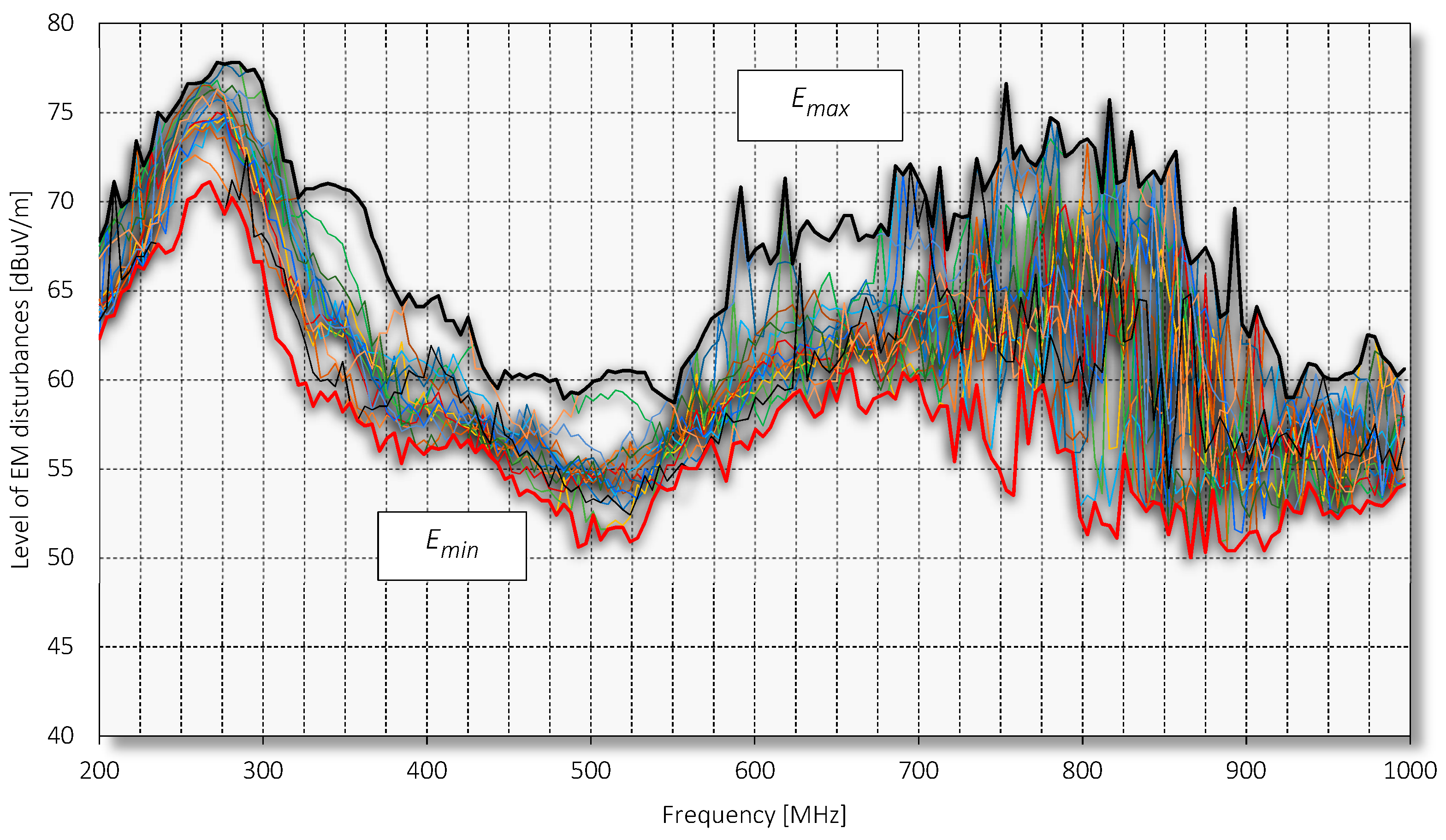
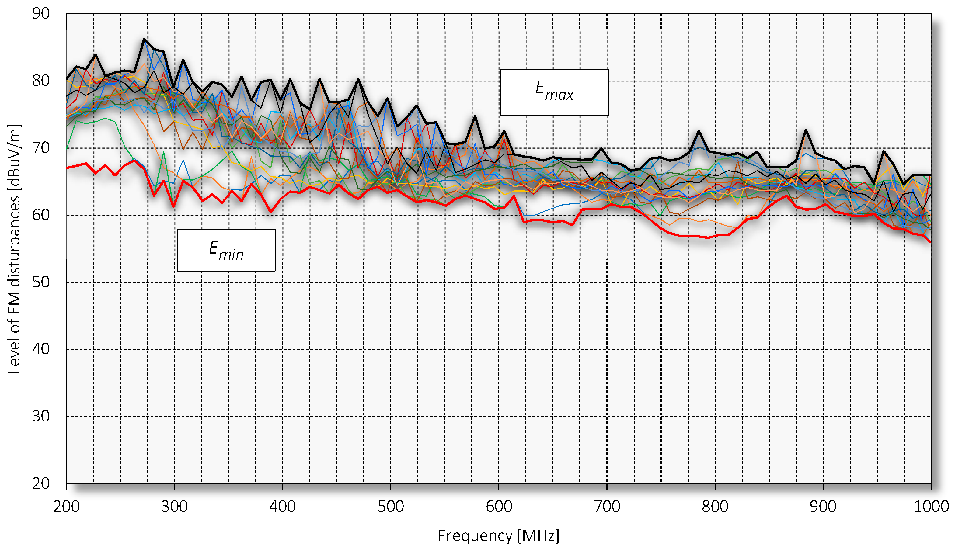
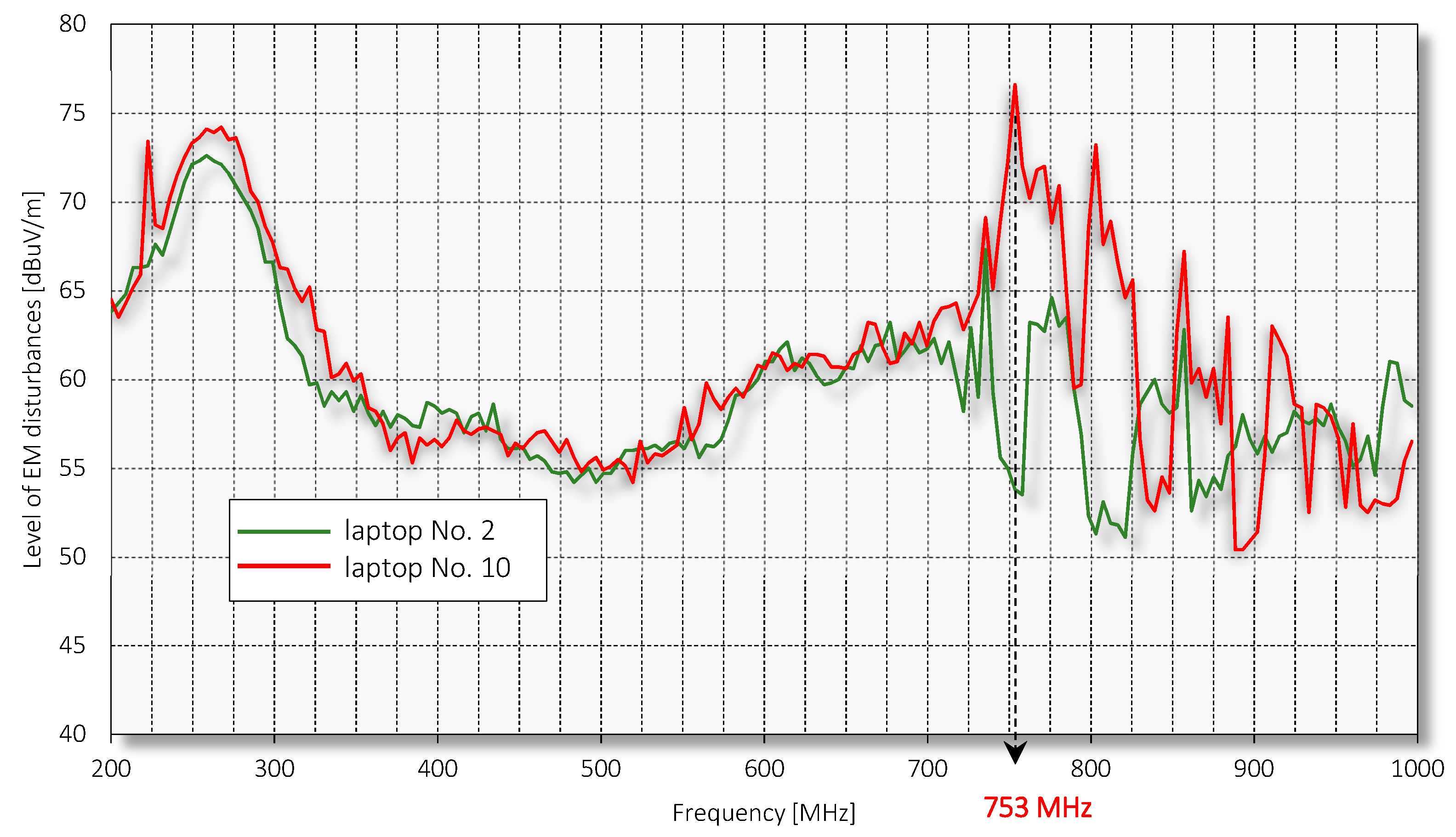
3. Results

Test results for each type of device were placed on a single graph (Figure 5, Figure 6, Figure 7, Figure 8 and Figure 9). This enabled easy analysis of levels of electromagnetic disturbances, as well as valuable emissions and assessment of observed risk [15,16,17]. Maximal Emax and minimal Emin values of electromagnetic disturbances:
E m a x ( f n ) = m a x [ E k ( f n ) ]
E m i n ( f n ) = m i n [ E k ( f n ) ]
where Ek—electromagnetic disturbances for k device (k = 1, 2, ..., K, K = 15), f—frequency, were marked with wider lines.
Laptop A Type
Figure 5. Levels of electromagnetic disturbances (valuable emissions, 15 measured devices of the same type) measured for laptop A in the range of frequencies from 200 MHz to 1 GHz, BW = 50 MHz, measurement distance: 1 m.
Electronics 08 01054 g005
Laptop B Type
Figure 6. Levels of electromagnetic disturbances (valuable emissions, 15 measured devices of the same type) measured for laptops B in the range of frequencies from 200 MHz to 1 GHz, BW = 50 MHz, measurement distance: 1 m.
Electronics 08 01054 g006
Laptop C Type
Figure 7. Levels of electromagnetic disturbances (valuable emissions, 15 measured devices of the same type) measured for laptops C in the range of frequencies from 200 MHz to 1 GHz, BW = 50 MHz, measurement distance: 1 m.
Electronics 08 01054 g007
Desktop A Type
Figure 8. Levels of electromagnetic disturbances (valuable emissions, 15 measured devices of the same type) measured for desktops A in the range of frequencies from 200 MHz to 1 GHz, BW = 50 MHz, measurement distance: 1 m.
Electronics 08 01054 g008
Desktop B Type
Figure 9. Levels of electromagnetic disturbances (valuable emissions, 15 measured devices of the same type) measured for desktops B in the range of frequencies from 200 MHz to 1 GHz, BW = 50 MHz, measurement distance: 1 m.
Electronics 08 01054 g009

Differences and Average Values of Levels of Electromagnetic Disturbances

The analysis of the test results of the levels of electromagnetic disturbances was conducted based on differences EDiff between maximum Emax and minimum Emin values for a given type of device (Figure 10 and Figure 11):
E D i f f ( f n ) = E m a x ( f n ) E m i n ( f n ) ,
As well as on the basis of average values EAvr for different types of devices (Figure 12 and Figure 13):
E A v r ( f n ) = k = 1 K E k ( f n ) K
Based on obtained results, the potential impact of the quality of electronic components of the devices on the levels of EM disturbances, as well as the electromagnetic protection level of processed information, can be noticed.

4. Discussions

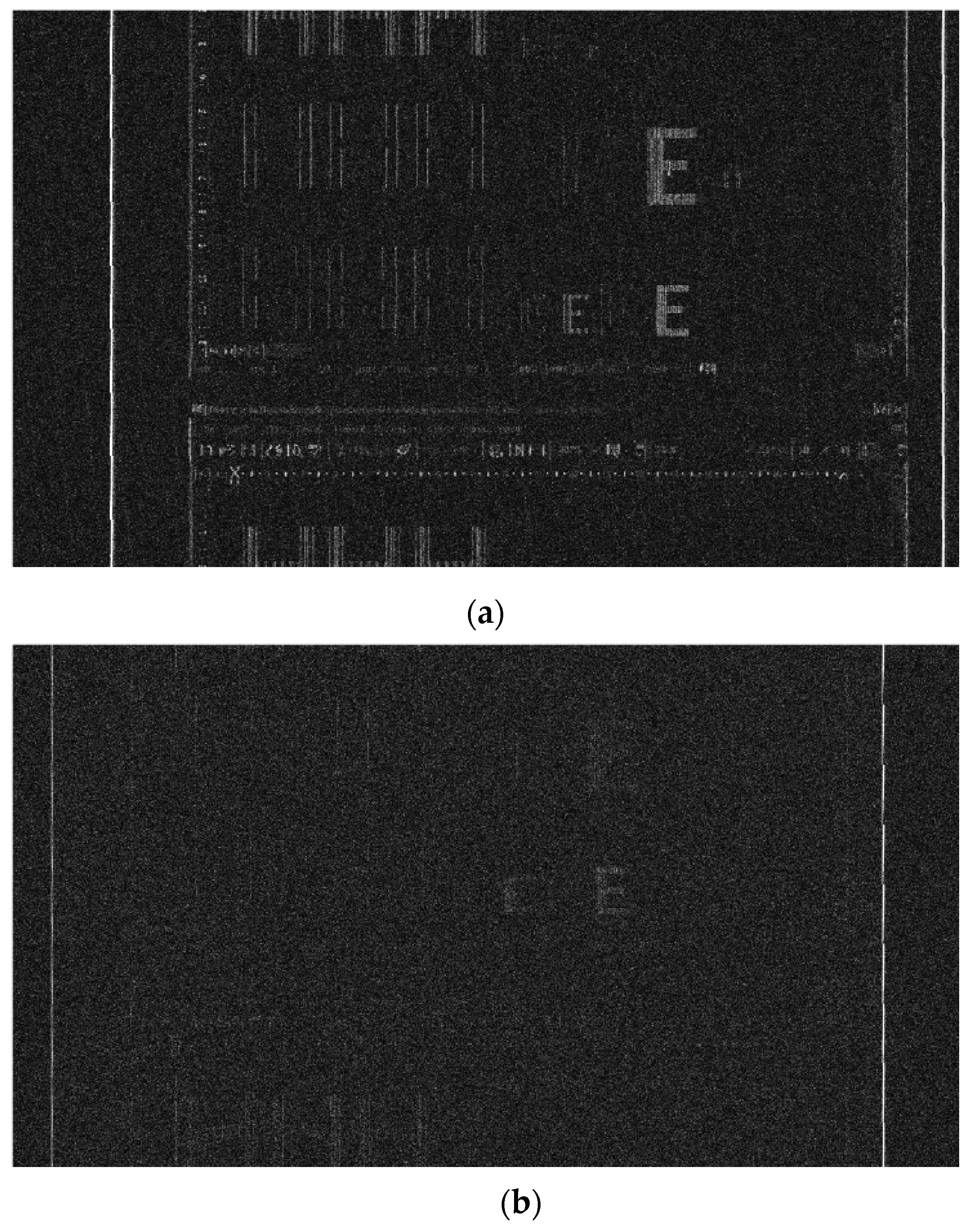
4.1. Valuable Emissions

The electromagnetic disturbances can have characteristics of processed information [18,19]. Such disturbances are called “valuable (sensitive) emissions”.
In this case, an increase of levels of measured emission by approximately several dB could enable the possibility of non-invasive acquisition of information (Figure 14) [20,21].
Examples of reconstructed images using recorded sensitive emissions on frequency 753 MHz for two different laptops of C type are shown in Figure 15.

4.2. Attenuation of Valuable Emissions

Analyzing Figure 14, it can be noticed that the difference of levels of electromagnetic emission, which appear on frequency 753 MHz, is very high (22.8 dB). This phenomenon allows reconstructing of primary information, and the information is legible. There can be selected other devices of the same type, which are characterized by lower levels of valuable emission. In this case, the emission does not allow reconstructing of primary information (Figure 16a). Of course, the first device can be used to process classified information. Then, many requirements have to be met, which decrease levels of sensitive emission (Figure 16b (zoning) and Figure 16c (zoning and shielding)). It is not easy. Different solutions have to be connected, which could make difficult the use of such a device.
It is connected with special zones and the shielding which have to ensure an appropriate attenuation of electromagnetic emission, according to the formula (Figure 17, [22]):
E = A B D ( r 1 ) ;
E = A D ( r 2 ) ;
where:
D ( r x ) = 20 log ( r x r 0 ) [ d B ] ;
and
  • rx—distance r1 or r2;
  • A—unaccepted level of EM emission;
  • B—attenuation inserted by shielding;
  • D—attenuation inserted by distance rx.
  • The value of D depends on the shielding material.
In case of emission measured on frequency 753 MHz, and without additional shielding, a protection zone has to have a minimal radius according to a formula:
22.8 = 20 log ( r 2 ) ;
log ( r 2 ) = 22.8 20 = 1.14 ;
r2 = 101.14 = 13.8038 [m].
In practice, a radius equaling more than 13 m is very big. It means that the protection zone on the radius, 13.8038 m, has to be organized around our device, which processes classified information.

5. Conclusions

This paper analyzes levels of electromagnetic disturbances from different types of electronic devices. Obtained results were connected, with possibilities of existence of sensitive emissions correlating with processed data. Each device of a given type was measured in the same conditions.
The results were largely scattered. Differences between levels of electromagnetic disturbances reached nearly 25 dB, especially in the frequency range from 600 MHz to 900 MHz. The phenomenon is very disquieting. There are frequencies in which valuable emissions most often exist [23]. Of course, the emissions come from sources in a shape of graphic lines (e.g., cables) and circuits (e.g., graphic cards). Experience shows that increasing the level of sensitive emissions by approximately 5 dB could determine classification of these emissions. In this context, we can consider the impact of the quality of components of electronic devices.
The quality of components additionally impacts the levels of electromagnetic disturbances. The differences between levels of electromagnetic disturbances of approximately 20–25 dB can decide whether a device meets the requirements of the EMC Directive. Not every device meets the limit values of EMC standardizations.
Another phenomenon considered in the article is the threat of information loss. Devices of the same type can be classified as meeting the requirements of electromagnetic protection of processed information or not. For devices for which the levels of sensitive emissions exceed the permissible values, it is necessary to use additional organizational solutions for electromagnetic safety. Such a solution may be a physical protection zone with a very large radius that is not always possible to create, especially when the device processing classified data must be used in offices. As shown in the analysis carried out, it may be necessary to use protection zones with a radius of more than 10 m. Therefore, the best solution is to choose one device out of several that is characterized by lower levels of sensitive emissions. As such, the device will allow the processing of classified information by meeting both the requirements of the SDIP-27/2 document (NATO TEMPEST requirements and Evaluation procedures) and the EMC directive.

Funding

This research received no external funding.

Conflicts of Interest

The author declare no conflict of interest.

References

  1. Lee, H.K.; Kim, J.H.; Kim, S.C. Emission Security Limits for Compromising Emanations Using Electromagnetic Emanation Security Channel Analysis. IEICE Trans. Commun. 2639, 10, 2639–2649. [Google Scholar] [CrossRef]
  2. Xie, C.h.; Wang, T.; Hao, X.; Yang, M.; Zhu, Y.; Li, Y. Localization and Frequency Identification of Large-Range Wide-Band Electromagnetic Interference Sources in Electromagnetic Imaging System. Electronics 2019, 8, 499. [Google Scholar] [CrossRef]
  3. Zhang, N.; Lu, Y.H.; Cui, Q.; Wang, Y.Y. Investigation of Unintentional Video Emanations from a VGA Connector in the Desktop Computers. IEEE Trans. Electromagn. Compat. 2017, 59, 1826–1834. [Google Scholar] [CrossRef]
  4. Glowacz, A.; Glowacz, Z. Diagnostics of stator faults of the single-phase induction motor using thermal images, MoASoS and selected classifiers. Measurement 2016, 93, 86–93. [Google Scholar] [CrossRef]
  5. Yuan, K.; Grassi, F.; Spadacini, G.; Pignari, S.A. Crosstalk-Sensitive Loops and Reconstruction Algorithms to Eavesdrop Digital Signals Transmitted Along Differential Interconnects. IEEE Trans. Electromagn. Compat. 2017, 59, 256–265. [Google Scholar] [CrossRef]
  6. Kubiak, I. Video signal level (colour intensity) and effectiveness of electromagnetic infiltration. Bull. Pol. Acad. Sci. – Tech. Sci. 2016, 64, 2007–2018. [Google Scholar] [CrossRef]
  7. Loughry, J.; Umphress, D.A. Information Leakage from Optical Emanations. ACM Trans. Inf. Syst. Secur. 2002, 5, 262–289. [Google Scholar] [CrossRef]
  8. Kubiak, I. Laser printer as a source of sensitive emissions. Turk. J. Electr. Eng. Comput. Sci. 1354, 26, 1354–1366. [Google Scholar]
  9. Cihan, U.; Aşık, U.; Cantürk, K. Analysis of Information Leakages on Laser Printers in the Media of Electromagnetic Radiation and Line Conductions. In Proceedings of the International Conference on Information Security and Cryptology, Ankara, Turkey, 30–31 October 2015. [Google Scholar]
  10. Wu, C.; Gao, F.; Dai, H.; Wang, Z.A. Topology-Based Approach to Improve Vehicle-Level Electromagnetic Radiation. Electronics 2019, 8, 364. [Google Scholar] [CrossRef]
  11. Jurič, I.; Nedeljković, U.; Novaković, D.; Pinćjer, I. Visual experience of noise in digital images. Tehnicki Vjesnik-Technical Gazette 2016, 23. [Google Scholar] [CrossRef] [Green Version]
  12. Tajima, K.; Ishikawa, R.; Mori, T.; Suzuki, Y.; Takaya, K. A study on risk evaluation of countermeasure technique for preventing electromagnetic information leakage from ITE. In Proceedings of the International Symposium on Electromagnetic Compatibility EMC Europe, Angers, France, 4–7 September 2017. [Google Scholar] [CrossRef]
  13. Telecommunication Standardization Sector of ITU. K.115: Mitigation methods against electromagnetic security threats. Available online: https://www.itu.int/rec/T-REC-K.115-201511-I (accessed on 16 September 2019).
  14. Kuhn, M.G. Compromising Emanations: Eavesdropping Risks of Computer Displays. Technical Report. 2003. Available online: http://www.cl.cam.ac.uk/TechReports/ (accessed on 16 September 2019).
  15. Cakir, G.; Cakir, M.; Sevgi, L. Electromagnetic radiation from multilayer printed circuit boards: a 3D FDTD-based virtual emission predictor. Turk. J. Electr. Eng. Comput. Sci. 2009, 17, 315–326. [Google Scholar]
  16. Litao, W.; Bin, Y. Analysis and Measurement on the Electromagnetic Compromising Emanations of Computer Keyboards. In Proceedings of the Seventh International Conference on Computational Intelligence and Security, Sanya, Hainan, China, 3–4 December 2011; pp. 640–643. [Google Scholar]
  17. Ko, W.L. Time Domain Solution of Electromagnetic Problems. Electromagnetics 1992, 12, 403–433. [Google Scholar]
  18. Kubiak, I. The Influence of the Structure of Useful Signal on the Efficacy of Sensitive Emission of Laser Printers. Measurement 2018, 119, 63–76. [Google Scholar] [CrossRef]
  19. Chervyakov, N.; Lyakhov, P.; Kaplun, D.; Butusov, D.; Nagornov, N. Analysis of the Quantization Noise in Discrete Wavelet Transform Filters for Image Processing. Electronics 2018, 7, 135. [Google Scholar] [CrossRef]
  20. Kubiak, I. LED printers and safe fonts as an effective protection against the formation of unwanted emission. Turk. J. Electr. Eng. Comput. Sci. 2017, 25, 4268–4279. [Google Scholar] [CrossRef]
  21. Kubiak, I. TEMPEST font counteracting a non-invasive acquisition of text data. Turk. J. Electr. Eng. Comput. Sci. 2018, 26, 582–592. [Google Scholar] [CrossRef]
  22. Telecommunication Standardization Sector of ITU. Test methods and guide against information leaks through unintentional electromagnetic emissions. Available online: https://www.itu.int/rec/T-REC-K.84-201101-I/en (accessed on 16 September 2019).
  23. Kubiak, I. Influence of the method of colors on levels of electromagnetic emissions from video standards. IEEE Trans. Electromagn. Compat. 2018, 61, 1–9. [Google Scholar] [CrossRef]
Figure 1. A photograph of the countermeasure device connected to a mobile PC.
Electronics 08 01054 g001
Figure 2. (a) A picture of the filtered fonts [14], (b) a picture for signal with limited spectrum [14].
Electronics 08 01054 g002
Figure 3. An anechoic chamber.
Electronics 08 01054 g003
Figure 4. Test system.
Electronics 08 01054 g004
Figure 10. Differences of measured levels of electromagnetic (EM) disturbances (valuable emissions) for three types of laptops in the range of frequencies from 200 MHz to 1 GHz.
Electronics 08 01054 g010
Figure 11. Differences of measured levels of EM disturbances (valuable emissions) for two types of desktop computers in the range of frequencies from 200 MHz to 1 GHz.
Electronics 08 01054 g011
Figure 12. Average values of EM disturbances (valuable emissions) for three measured laptops in the range of frequencies from 200 MHz to 1 GHz.
Electronics 08 01054 g012
Figure 13. Average values of EM disturbances (valuable emissions) for two measured desktop computers in the range of frequencies from 200 MHz to 1 GHz.
Electronics 08 01054 g013
Figure 14. Levels of electromagnetic emissions from two selected laptops C and frequency of valuable emissions in the range of frequencies from 200 MHz to 1 GHz.
Electronics 08 01054 g014
Figure 15. Reconstructed images for valuable emissions measured on frequency 753 MHz for two laptops type C: (a) laptop No. 10, (b) laptop No. 2.
Electronics 08 01054 g015
Figure 16. Attenuation methods of emission from electronic device: (a) equipment class A and protection zone about radius r0 = 1 m, (b) equipment class B and protection zone about radius r2 > r1 > r0, (c) equipment class B inside of shielding and protection zone about radius r1.
Electronics 08 01054 g016
Figure 17. Attenuation of emission from electronic device
Electronics 08 01054 g017

