1. Introduction
Since the appearance of the first high-efficiency blue LEDs in 1993, solid-state lighting devices have experienced a strong advance. In the last few years, almost every technical feature of LEDs has been greatly improved. For example, the evolution of the semi-conductor technology used to produce blue light, together with the improvement of the characteristics of the phosphors used to turn that blue light into the desired white light, allow obtaining a color spectrum suited even for applications where exceptional color reproduction is required (e.g., illumination of paintings). On the other hand, the optics used nowadays in LED lamps allow obtaining wide light beams with a good color consistency across the entire illuminated area [
1]. The thermal behavior and the light depreciation along the LED life have also been improved thus making possible the construction of high power modules [
2,
3]. For example, there can be found currently in the market chip-on-board (COB) LED modules of more than 200 W. Another important feature of LEDs is their fast response and ease of control, enabling the implementation of complex control strategies [
4,
5,
6]. All these improvements, combined with the continuous cost reduction that has taken place in recent years, have made LEDs the preferred choice for most lighting applications nowadays.
The availability of better light sources has also been considered by many public administrations to push the specifications required for new installations to higher levels [
7,
8]. Furthermore, even the metrics used to characterize light sources have had to adapt to the new possibilities associated with the use of solid-state lighting systems. For example, the color rendering index (CRI) is considered insufficient to characterize the color reproduction of a light source based on LEDs. Many manufacturers are using the color metrics described in IES TM-30-18 in their product datasheets [
9]. In the same way, new light flicker standards have also appeared setting stricter limits that could hardly be met using traditional lighting systems (e.g., IEEE 1789 [
10]).
The need to comply with both the input harmonic and the output flicker standards have led manufacturers to lean towards two-stage topologies. The first stage is used for power factor correction (PFC) and is needed to comply with the standard IEC 61000-3-2. The second stage is used to control the LED current and minimize the light flicker.
The most commonly used topologies for PFC in solid-state lighting systems are the flyback and boost converters. However, in the bibliography there can be found examples where almost every topology suited for PFC are used as well [
11,
12]. The second stage can be used for several purposes: flicker reduction, current balancing across multiple LED strings, adding dimming capability, or implementing light modulation techniques for visible light communications [
13]. Different solutions can be found in the literature concerning these mentioned features. For instance, current equalization in multi-string LED lamps can be performed by optimized dissipative solutions [
14] as well as by specific power topologies that maximize the efficiency [
15]. When the main goal is to control the LED current in order to either provide dimming or to eliminate the low frequency flicker, there are solutions based in resonant [
16] and non-resonant configurations [
17,
18]. In some designs, the bulk capacitor required in the first stage for PFC is made using plastic film instead of electrolytic capacitors. In this case, the second stage has to handle a greater input voltage ripple in order to reduce the size of the required capacitor. This change allows increasing the driver lifetime compared to using a low-cost electrolytic capacitor [
19,
20].
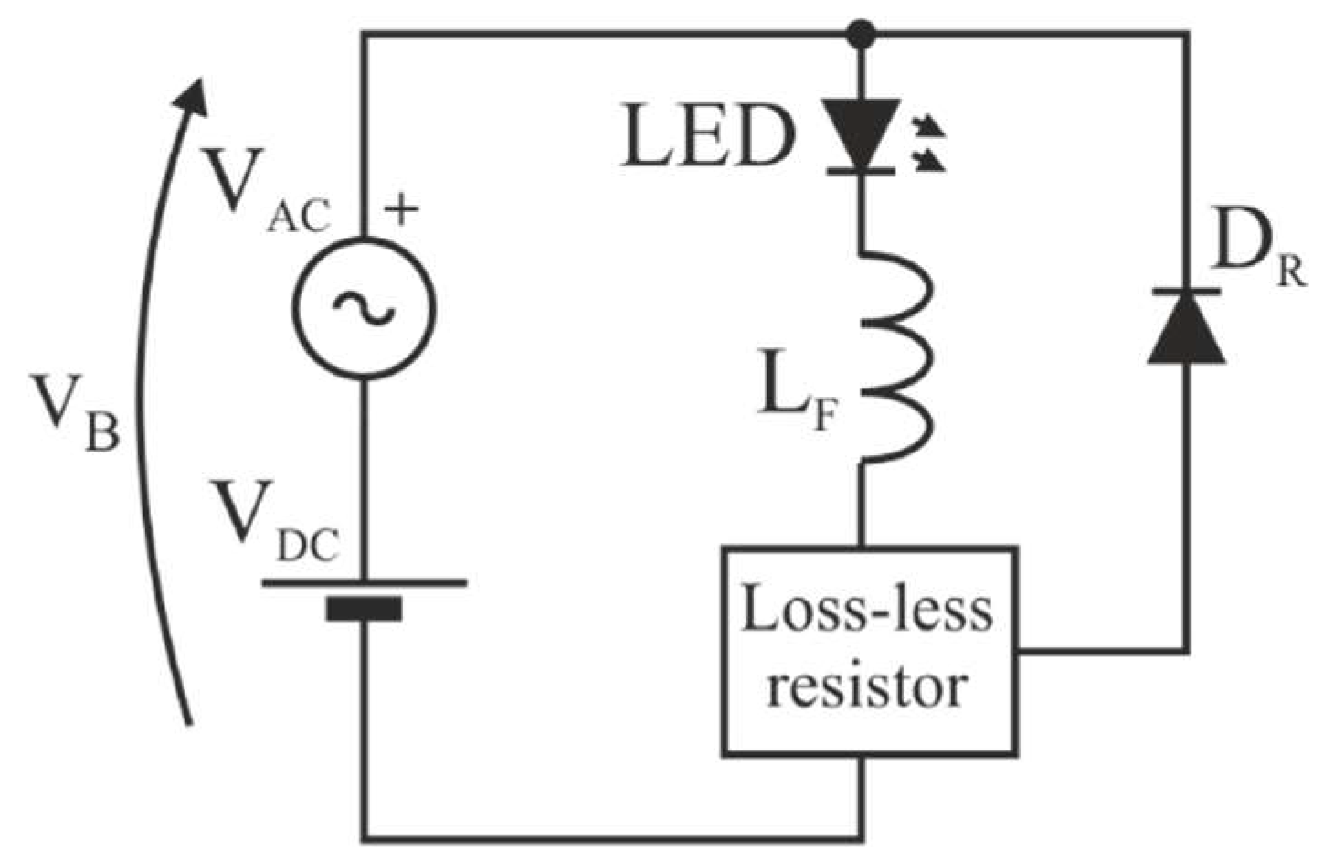
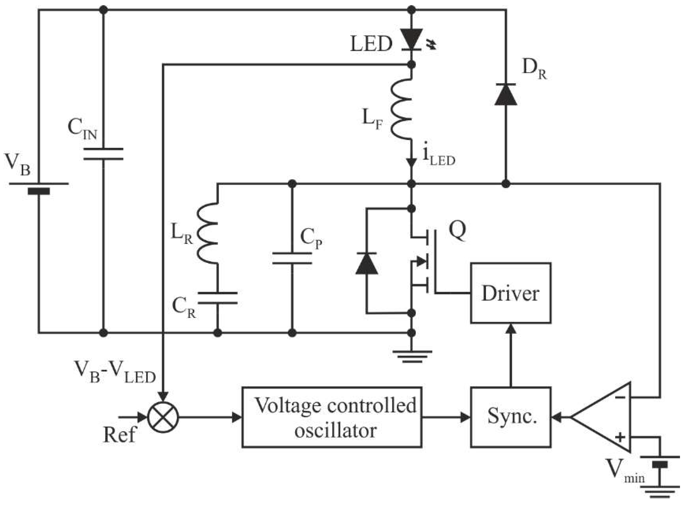
Present work describes a new resonant topology especially suited for this purpose. The proposed circuit is based on the series regulator concept described in
Figure 1. The current through the LED is controlled by a filter inductance L
F followed by a high frequency converter that behaves as a variable loss-less resistor. The power handled by this converter is sent back to the input by means of the recycling diode D
R. The amount of power recycled will be directly related to the converter voltage ratio. If the input and output voltages are equal the power recycled will be null.
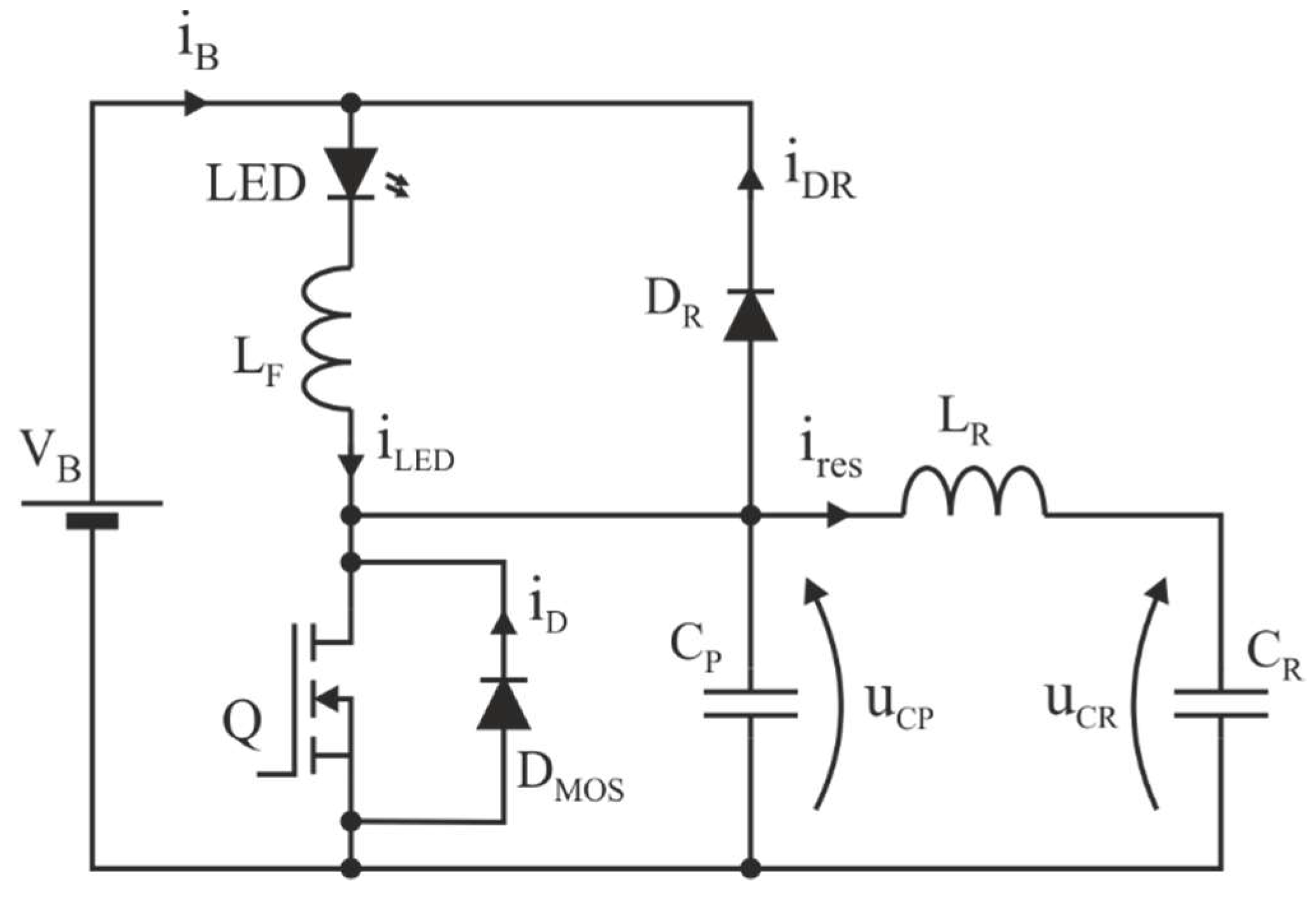
The simplified schematic of the proposed topology is shown in
Figure 2. This topology can be derived from two different basic topologies: the buck DC–DC converter or the class-E inverter. One of the techniques used in the bibliography to derive resonant converters from standard DC–DC configurations is based on adding resonant networks. These networks are used to reduce switching losses thus enabling the possibility to operate at higher frequencies without compromising the efficiency [
21,
22]. The proposed topology can be derived from a buck converter by adding a soft-switching resonant network consisting of two branches in parallel: one formed only by capacitor C
P, and another by the inductance L
R in series with capacitor C
R (See
Figure 2).
In this circuit, L
R and C
R constitute the main resonant network, handling an almost sinusoidal current i
res. This current allows a smooth charge and discharge of capacitor C
P between zero and the bus voltage V
B. The key aspect for proper operation of this circuit is to ensure a complete discharge of capacitor C
P before the switch Q is turned on. If this zero-voltage-switching (ZVS) condition is not met, the efficiency will drop significantly as the energy stored in C
P at turn-on will be dissipated in the mosfet, causing strong current spikes. On the other hand, capacitor C
P ensures a small dv/dt across transistor Q during the turn-off transient thus reducing the switch-off losses. This behavior is also found in the standard Class-E inverter configuration, allowing these circuits to be used at very high frequencies [
23].
One of the main disadvantages of the Class-E inverter and some similar topologies [
16], is the high peak-to-average ratio of the mosfet voltage. In many designs, this ratio can be higher than five making necessary the use of high-voltage transistors. In the proposed topology, the maximum voltage across the mosfet is equal to the bus voltage V
B due to the addition of the clamping diode D
R. Similar alternatives where explored in the bibliography for other circuit configurations not intended for LED supply [
24].
The most similar topology described in prior literature is the modified Class-E converter found in [
16]. In this circuit, the AC output of a standard Class-E inverter is rectified and sent back to the input obtaining a DC–DC series regulator. However, no voltage clamping is used and the mosfet voltage can be considerably higher.
The remainder of the paper will be organized as follows. In first place, a detailed description of the operation of the proposed circuit will be made. This description will be followed by a simplified analysis based on the fundamental approach. The resonant current iRES will be approximated as a pure sinusoidal signal to obtain a set of design charts. In section four, basic hints to design a circuit based in these charts will be discussed. Next, a sensitivity analysis will be carried out. This analysis is intended to provide a general idea on how the control must work to compensate for small-signal perturbations at the input or the load. Finally, the laboratory prototype will be described together with the experimental results obtained at different operating conditions. The main conclusions of this work will be given at the last section.
2. Circuit Operation
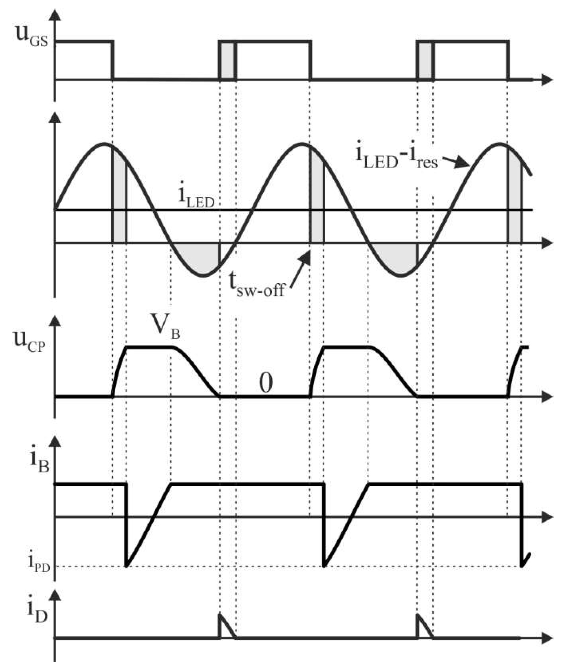
To simplify the circuit analysis, the resonant current will be approximated as a pure sinusoidal signal and the LED current ripple will be neglected.
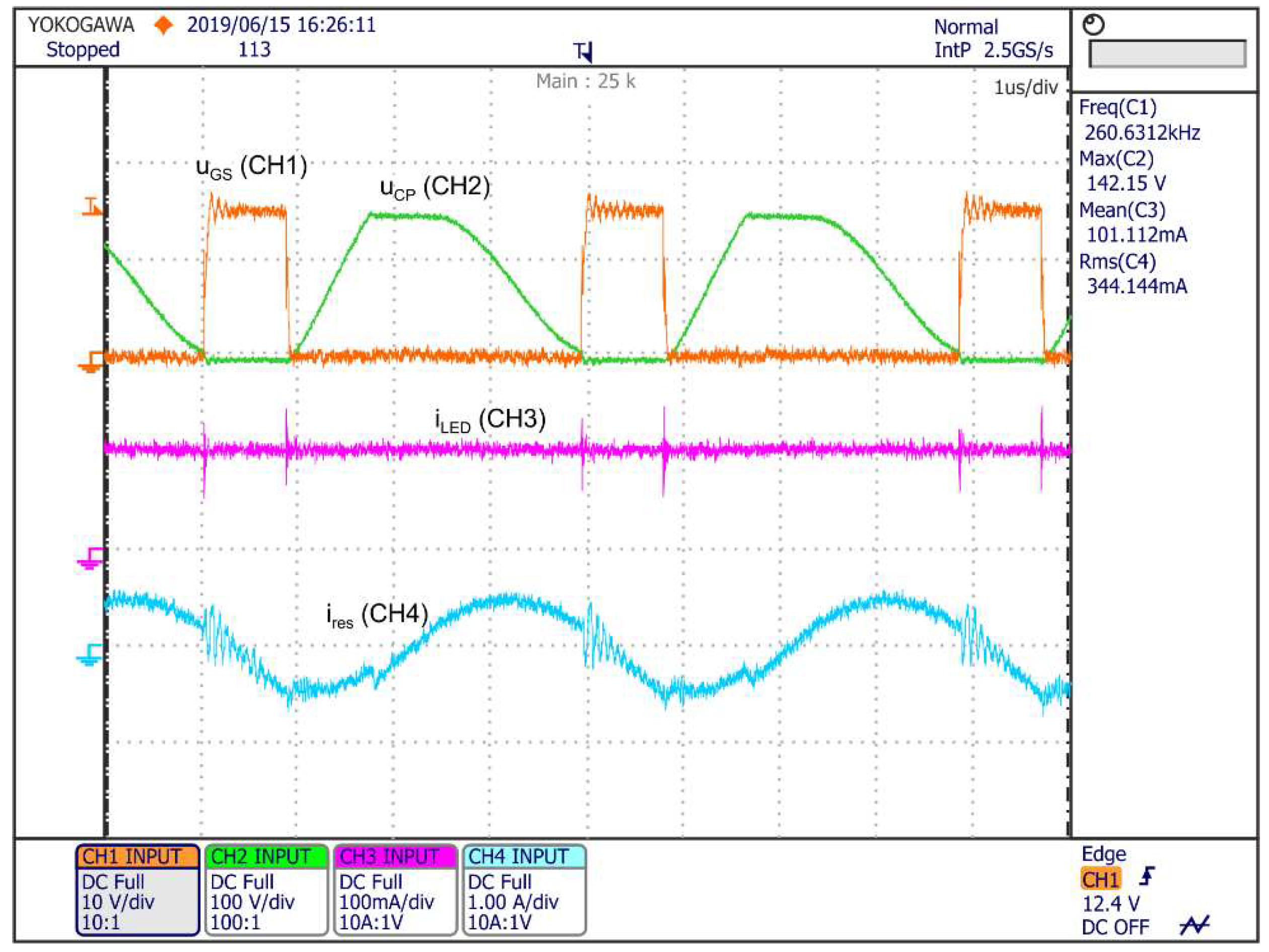
Figure 3 shows the main waveforms of the proposed circuit based in those assumptions. The most important trace to understand how the circuit operates is the i
LED-i
res shown in second place. When the transistor is switched-off (indicated as t
sw-off in the figure), capacitor C
P starts charging until it reaches the bus voltage V
B. Once this happens, the clamping diode D
R starts conducting. During this interval, the current handled by this diode is equal to i
LED-i
res, and the current through the source i
B is equal to the resonant current i
res, thus providing a steep change in the input current at the instant when the clamping diode starts conducting. When i
LED-i
res goes down to zero, the clamping diode turns off. At this point, voltage u
CP starts decreasing due to its negative current balance (negative shaded area). Once C
P is completely discharged, the current starts flowing through the mosfet body diode. The transistor should be turned on before this condition is lost in order to achieve ZVS. When the clamping diode is in the off state, the current handled by the input source is equal to the LED current i
LED.
3. Circuit Analysis Based on the Fundamental Approach
To obtain the simplified equations and design charts that describe the circuit operation the next four steps will be followed:
Identify the angles where changes in the operating mode take place
Obtain the normalized expression of the mosfet voltage uCP
Determine the relations between angles and normalized circuit parameters
Numerically solve the set of non-linear equations and depict the normalized design charts.
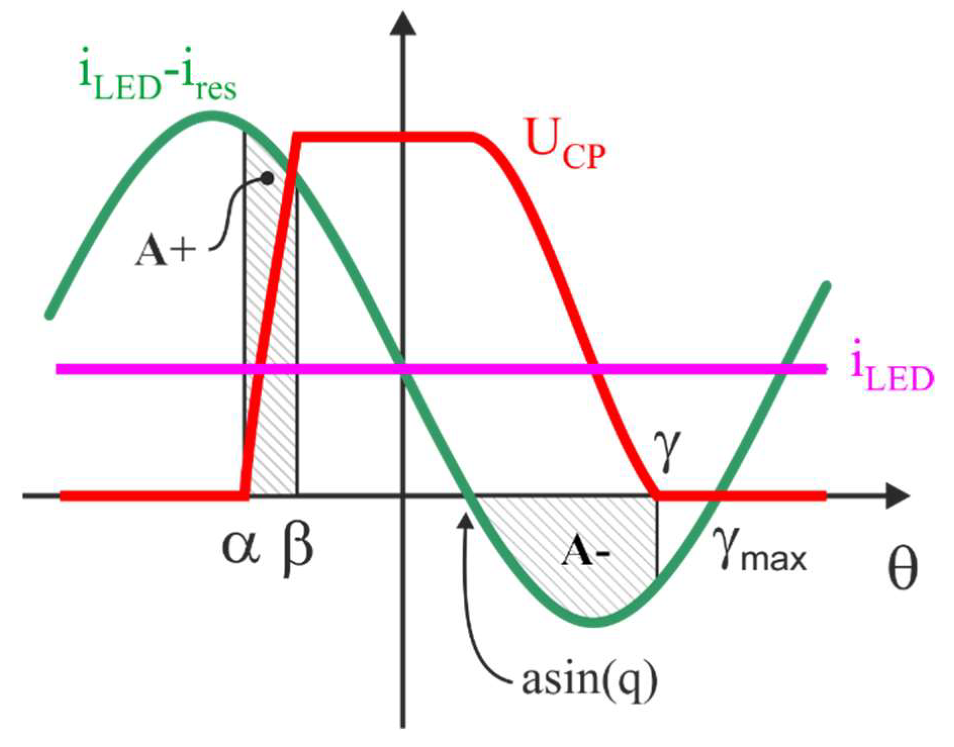
The detailed representation of the main circuit waveforms during one switching cycle is shown in
Figure 4.
In this figure, the angle reference is set at the zero crossing of the resonant current.
α angle defines the point where the transistor switches off.
β is the angle where
CP reaches the bus voltage and the clamping diode
DR turns on. When the current
iLED-
ires becomes negative (at
asin(
q)), capacitor
CP starts discharging until it reaches zero at
γ angle. The positive and negative shaded areas marked as A+ and A− in
Figure 4 must be equal at steady state, as the average capacitor current is null. This condition cannot be fulfilled if the angle
γ is greater than the
γmax angle indicated in the figure.
This behavior can be described by the following formula:
where
ω corresponds with the operating angular frequency and
Ires(peak) is the
peak value of the resonant current. To normalize the previous expression, parameter
q will be defined as:
Expression (1) can then be transformed into:
by means of the following definition:
The normalized expression of the bus voltage
MB can be calculated using:
There are several restrictions that apply to Expression (3). These restrictions can be used to obtain a set of three equations that define the basic relations between circuit parameters. These equations will be used to obtain the main design charts.
In first place, the voltage balance across
CP capacitor means that areas A+ and A− must be equal, (see
Figure 4). This condition provides the following equation:
The second equation will be obtained by means of the input-to-output power balance. Considering that the input and output powers must be equal, the following formula is obtained:
where parameter
ĸ is defined as:
The third equation will be obtained using the restriction that comes from the fact that the L
R-C
R resonant tank cannot handle active power. Therefore, the
MCP component of the fundamental harmonic that is in phase with the resonant current must be zero:
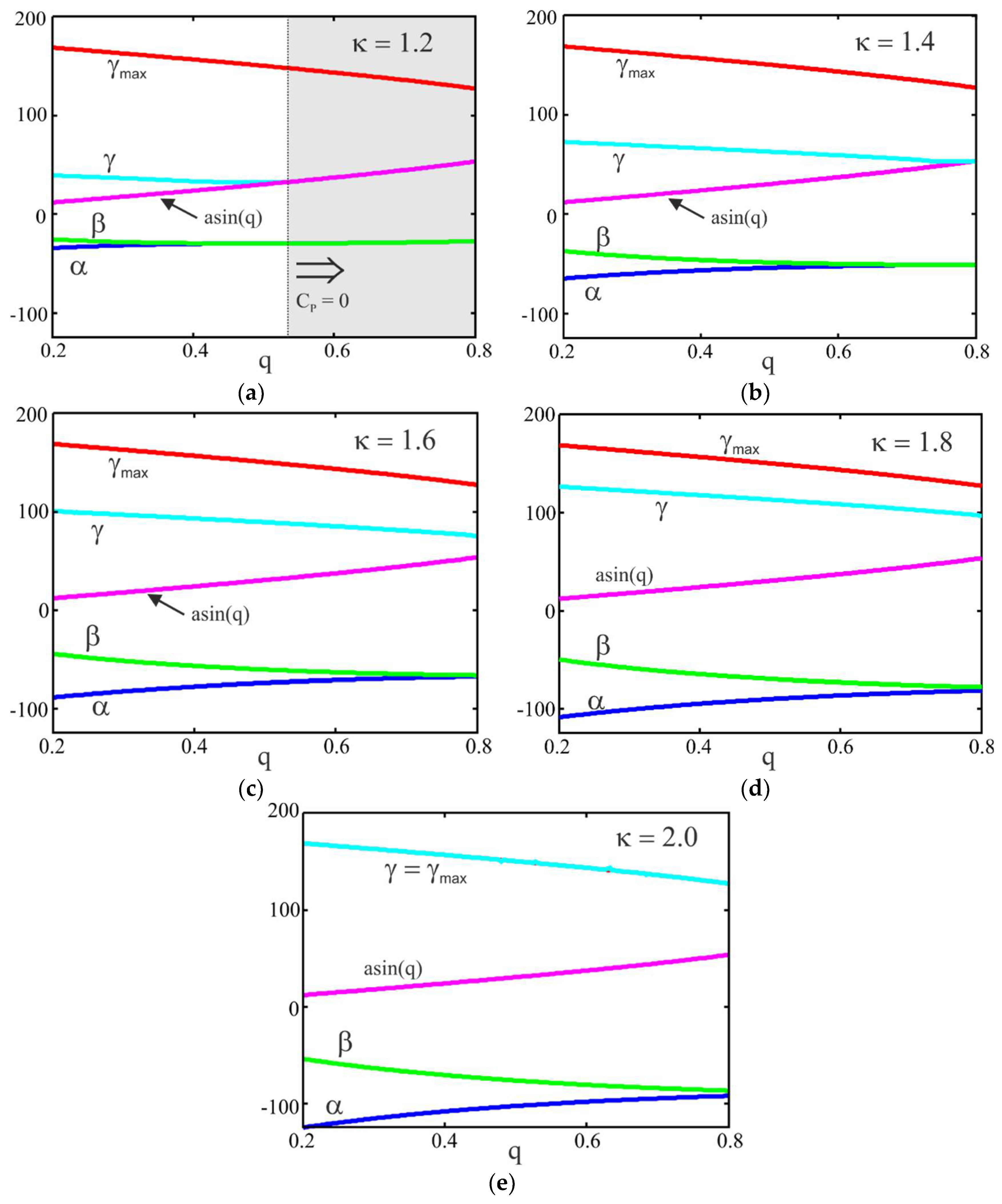
Expressions (6), (7), and (9) are defined as functions of 5 parameters, that is: q, α, β, γ, and ĸ.
These three equations allow to determine the angles that define the circuit operation (
α,
β, and
γ) as functions of parameters
q and
ĸ. The charts shown in
Figure 5 were obtained by numerically solving Equations (10)–(12) for different values of
q and
ĸ. According to theses charts, there are several conclusions that can be extracted. As it was stated before, transistor switch-on must take place between the instants defined by
γ and
γmax to achieve ZVS. For
ĸ = 2, as both angle values are coincident, there is no control margin and the transistor must be turned on at
γ.
Therefore,
ĸ = 2 defines the theoretical maximum ratio between the input and output voltages that can be used. For higher
ĸ values it is not possible to fully discharge capacitor
CP and maintain ZVS, giving rise to high switching losses. On the other hand, having a significant difference between
γ and
γmax means that the reactive power handled by the converter is high, increasing the losses in all circuit components. Besides, for small
ĸ values, the
q range that can be used is limited to the area where
α and
β are different thus the shaded area shown in
Figure 5a should be avoided.
In fact, one of the most important limitations of the proposed circuit is that the input-to-output ratio must be between 1.2 and 2 for proper operation.
4. Proposed Design Methodology
The best way to illustrate how the design can be made is by means of a practical example. For that purpose, a 40 W lamp with a rated voltage of 80V will be used. The lamp specifications and the basic circuit parameters of this example are summarized on
Table 1. The circuit will be used to reduce the low frequency ripple in the LED lamp and provide dimming capability. As it was addressed in previous section, parameter
ĸ must be between 1.2 and 2 for proper operation. In this example, the maximum
ĸ will be set at 1.9 and the minimum at 1.3, with a nominal value of 1.6. This allows handling a 16 V low frequency ripple with a nominal bus voltage of 128V.
In this example, based on our experience, the nominal
q value was set to 0.4, and the nominal operating frequency selected was 200 kHz. The nominal values of angles
α,
β and
γ can be obtained directly from
Figure 5.
In the next paragraphs, the procedure to calculate the main circuit parameters will be addressed. In first place, integrating Equation (1) between
α and
β the following relation is obtained:
where
R value is defined as:
This expression gives the
CP value shown in
Table 1. On the other hand, the
peak value of the fundamental component of voltage
UCP must be equal to the equivalent impedance of the
LR-
CR resonant tank (
Zres) multiplied by
Ires(peak). That is:
This relation can also be expressed as:
This expression can be used to calculate
Zres value at the nominal operating point. To determine the individual values of
LR and
CR an additional parameter must be defined:
Parameter ν corresponds to the ratio between the impedance at nominal frequency of the inductance LR referred to the impedance of CR.
Normally,
Zres impedance will have a dominant inductive behavior meaning that
ν should be greater than one. However, if this parameter is much bigger than one, the
LR-
CR will operate far from resonance and
ires will be highly distorted. On the other hand, if
ν is close to one, the circuit will be extremely sensitive to small changes in the operating frequency and tolerances in the component values. Besides, both
LR and
CR will handle higher voltages and present significantly higher losses. In this example, parameter
ν was set to a trade-off value of 1.5. The calculated values of
LR and
CR are shown in
Table 1.
Equation (15) can also be used to calculate the AC component of the voltage across the filter inductor LF. The minimum LF value to obtain a ripple below 10% across the LED is 1.2 mH. In this design the selected LF was 2 mH.
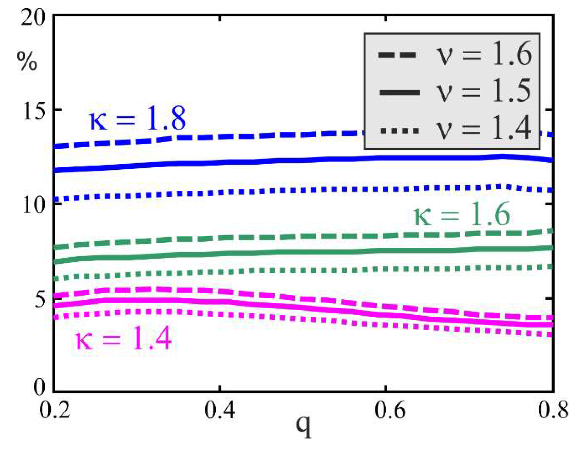
The fundamental approach has been used in all previous steps of the proposed analysis. The validity of this approach can be confirmed by comparing the amplitude of higher order harmonics with the fundamental. An estimation of this distortion can be made by assuming that the voltage
UCP can be approximated by Equation (1) even if there is a small distortion in the resonant current. Fourier analysis can then be used to estimate the higher order harmonics of
ires and compare them to the fundamental.
Figure 6 shows the ratio between the second harmonic and the fundamental as a percentage. As it can be observed, using the parameters of the previous example, the distortion of the second harmonic at nominal power is 7.3%, thus the error derived of using the fundamental approach is quite small.
5. Small Signal Analysis of Proposed Converter
As it was addressed before, the purpose of this circuit is to control the LED power with two objectives: reducing the low frequency ripple and providing dimming capability. Therefore, if either the bus or the lamp voltage change, the circuit must regulate the output power accordingly.
As in many resonant configurations, the only parameter that can be used to control the operating point of the proposed converter is the switching frequency. In this section, the non-linear equations obtained previously will be linearized in order to obtain the circuit sensitivity against changes in frequency, bus and lamp voltages.
To perform the small-signal analysis of the static characteristics, the Equations (10)–(12) will be combined with the Equations (13), (16), and (18). These last three equations were used to calculate
CP,
LR and
CR, and can also be written as:
In the remaining of this paper, the caret sign (^) will be used to identify small-signal variables, and sub-index ‘0′ will be used to indicate steady-state values of all variables.
The main goal of this analysis is to obtain the relation between the small-signal values of the lamp power
, lamp current
, lamp voltage
, bus voltage
and angular frequency
. To do so, some of the parameters used in previous equations must be calculated as functions of these five small-signal variables. In first place, using the Definition (8),
can be written as:
In a similar way, the lamp’s equivalent resistance can be expressed as:
Linearizing (17), the small-signal value
is found to be proportional to
:
Lamp power
can be expressed as a linear function of
and
:
Combining previous expressions and definitions the following small-signal matrix equation is obtained:
where
A and
B matrixes are defined as:
Using Equation (26) and Definitions (22)–(25) it is possible to obtain each small-signal variable as a linear function of
,
, and
. For example:
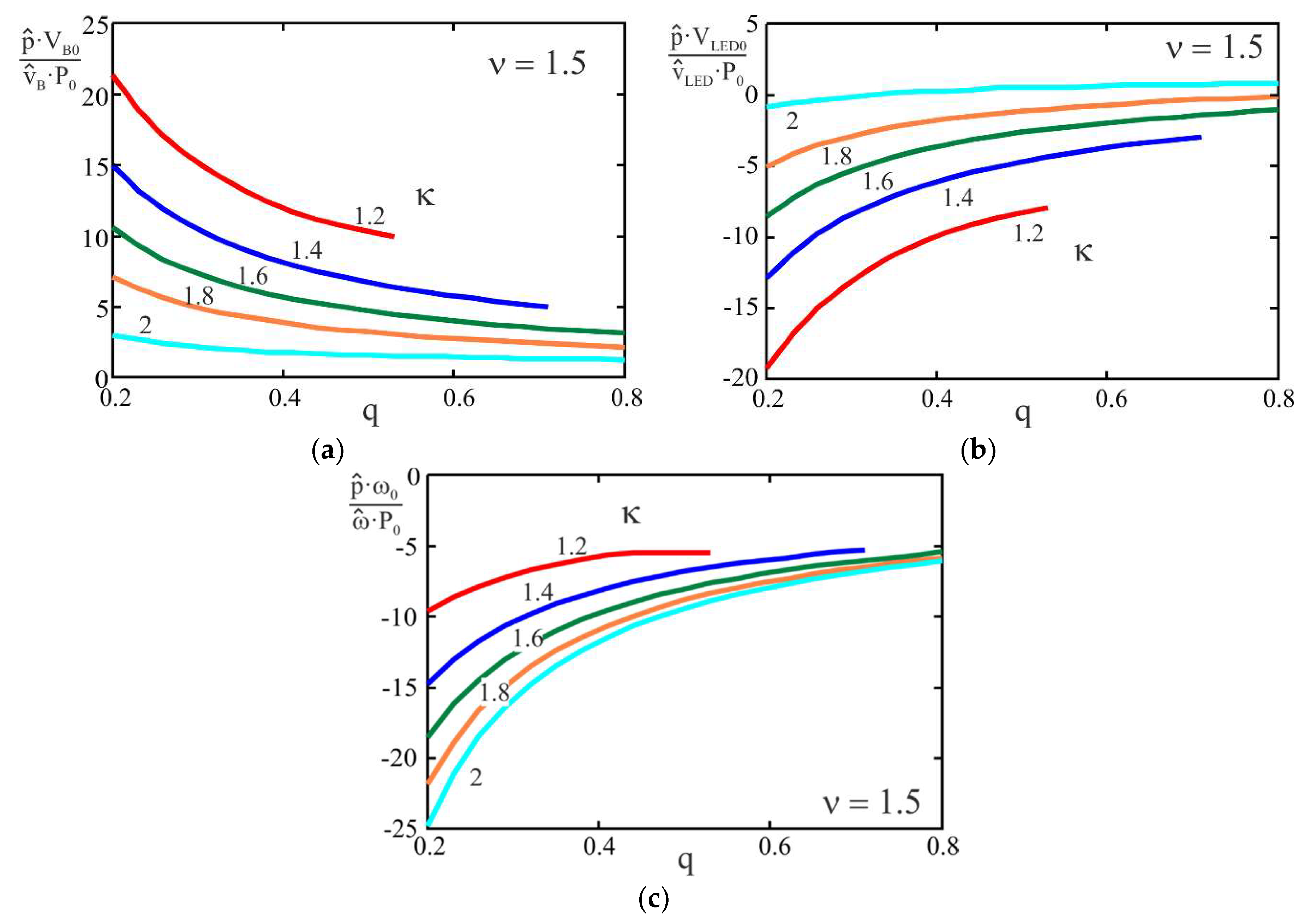
This equation, combined with (25), can be used to obtain the lamp power sensitivity charts shown in
Figure 7. These charts represent the ratio between the per-unit change in the lamp power
, referred to the per-unit change in
,
, and
, respectively.
One of the conclusions that can be extracted from these charts is that it is not possible to select an operating point where the power is independent of changes in the lamp voltage or the bus voltage. The best approach to this condition can only be obtained for ĸ close to two; but, as it was stated before, this should be avoided to maintain ZVS.
In the particular case of
q = 0.4 and
ĸ = 1.6 used in the example described in previous section, a power against bus voltage sensitivity value of 5.6 can be obtained from
Figure 7a. This value means that a variation of 1% in the bus voltage will lead to a change in the lamp power of 5.6%. Therefore, the operating point is extremely sensitive to changes at the converter input thus the control circuit must sense and compensate for changes in the bus voltage.
Figure 7c shows that the converter is highly sensitive to changes in the operating frequency. Therefore, the frequency excursion that will be required to control the operating point should be small. This is an interesting feature to minimize the size of the EMI filter that will be required.
To optimize the control, the most precise solution would be sensing the LED power and adjusting the switching frequency in closed loop. The main problem for its practical implementation would be sensing the lamp current. An expensive isolated DC current sensor will be needed as the lamp is not referred to ground. To overcome this limitation, a simple feedforward control is proposed in this work.
The main problem of the feedforward control is that both the bus and the LED voltages have to be measured independently and two different gains must be used to control the frequency against variations in both parameters. In the proposed topology, sensing the difference between
VB and
VLED is very easily done (see
Figure 8). Therefore, if the sensitivities of the lamp power with respect to both parameters are the same, this single measurement would allow to adjust the frequency using a single voltage-to-frequency gain.
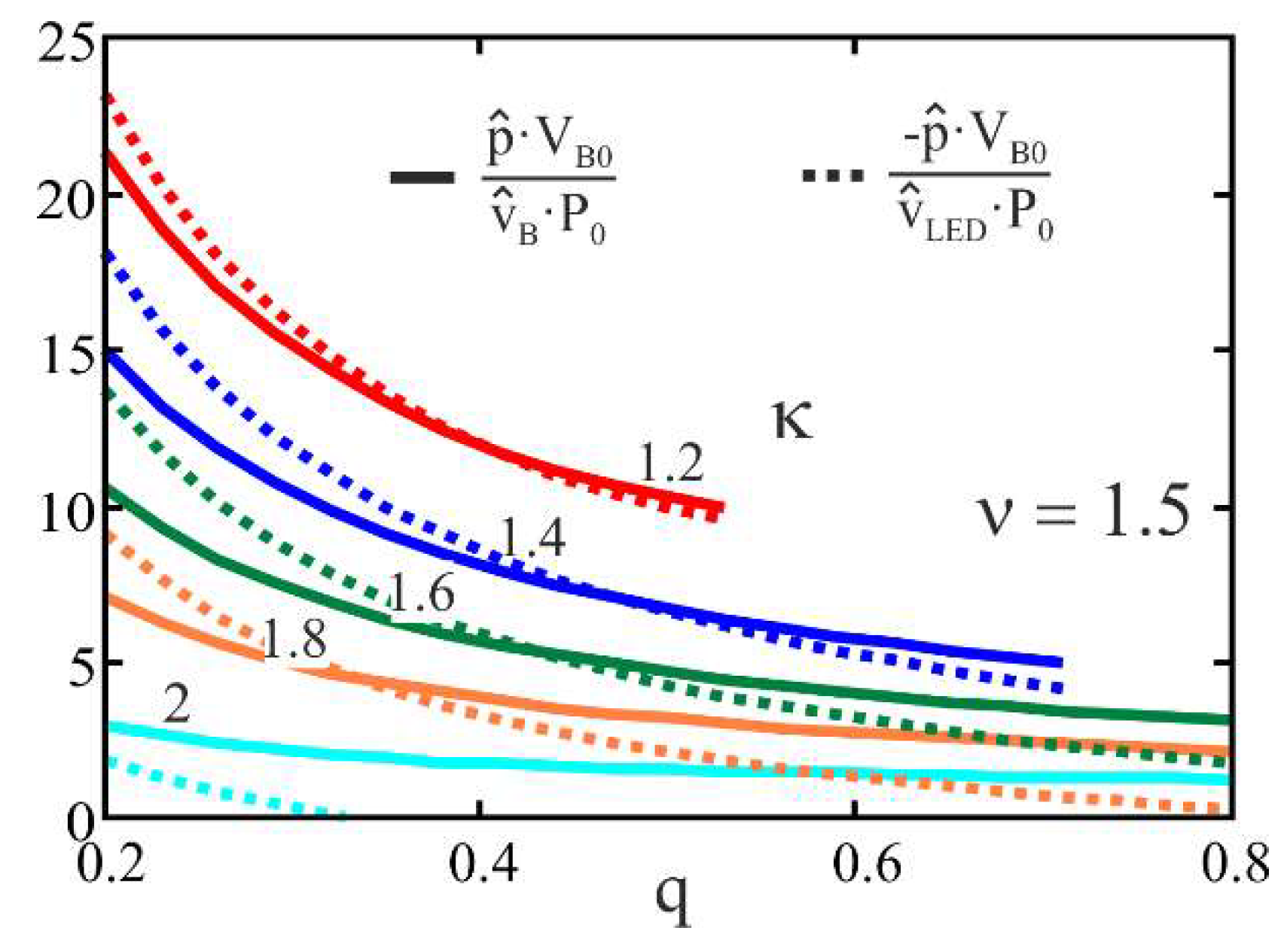
The frequency variation required to compensate for a change in the bus voltage (when
VLED is kept constant) can be calculated directly from
Figure 7a,c. With the proposed measurement, a change in
VLED cannot be distinguished from a change in
VB. However, if
is also referred to
VBUS0 instead of
VLED0 (multiplying by −
ĸ), the curves in
Figure 7b will be comparable to those in
Figure 7a. The small-signal power sensitivity charts against changes in
and
(both referred to
VBUS0) are shown in
Figure 9.
As it can be observed in the figure, for q = 0.4, ĸ = 1.6 and ν = 1.5, the dashed and solid lines are almost coincident thus the frequency change required to compensate a variation of 1 V in VB or −1 V in VLED will be approximately the same. This characteristic enables sensing VB-VLED instead of both signals independently. For other values of q, ĸ, and ν, this approximation will be less precise.
Due to the high di/dt values handled at the input of this converter is especially important placing a low ESR (equivalent series resistance) capacitor at the input (shown as
CIN in
Figure 8).
6. Design Analysis and Experimental Results
Using the design example described in
Section 4 and the control strategy described previously a laboratory prototype was built and tested. The main characteristics of the circuit components can be found on
Table 1.
Transistor switch-on was made by detecting the instant when capacitor
CP gets fully discharged. To do so, a threshold value close to zero was compared with
UCP. This value is shown in
Figure 8 as
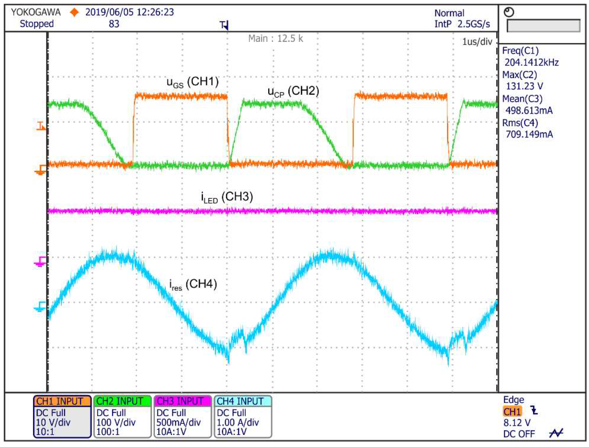
Vmin. This way, the time interval where the intrinsic mosfet diode is handling current is minimized, further reducing the conduction losses.
Figure 10 shows the main converter waveforms at the nominal operating point. As it can be seen, the ZVS condition is met and capacitor
CP is fully discharged when transistor switches on. The LED current has a negligible high frequency ripple due to the high value of the filter inductor
LF.
Figure 11 shows the circuit operating at maximum
VB and minimum
VLED, which corresponds to
ĸ = 2. It can be observed that the circuit is at the limit of ZVS and
CP is not fully discharged when the transistor switches on.
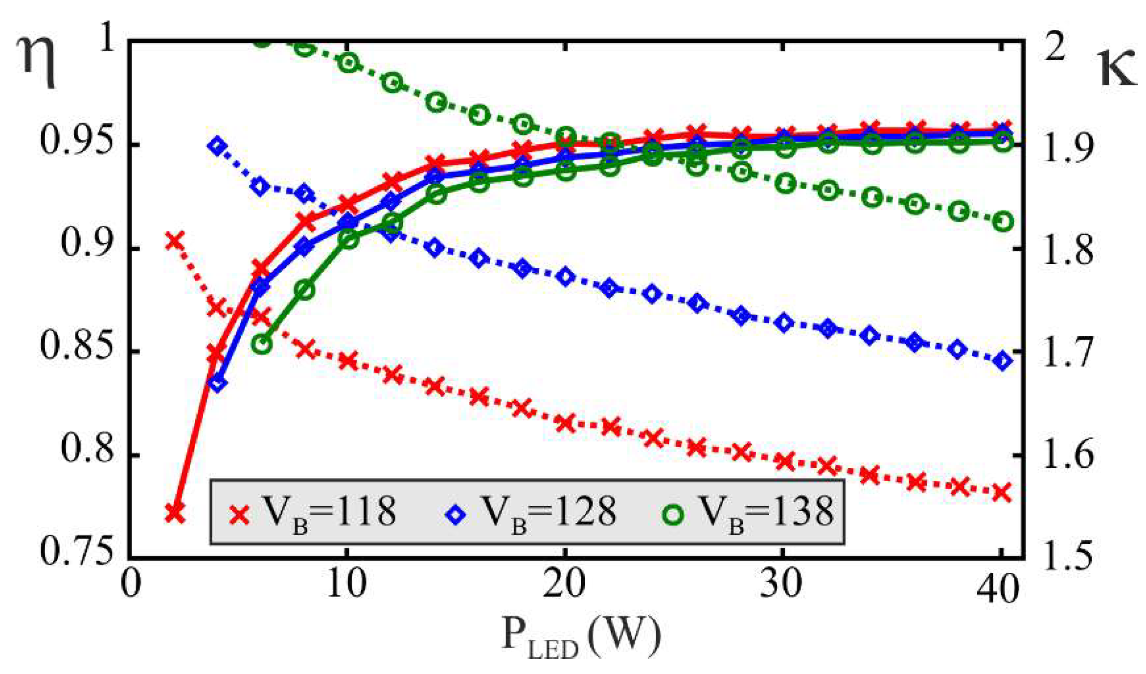
The circuit was also tested at different frequencies for three different values of the bus voltage. The efficiency was measured using a Yokogawa WT3000E Precision Power Analyzer and the results are summarized in
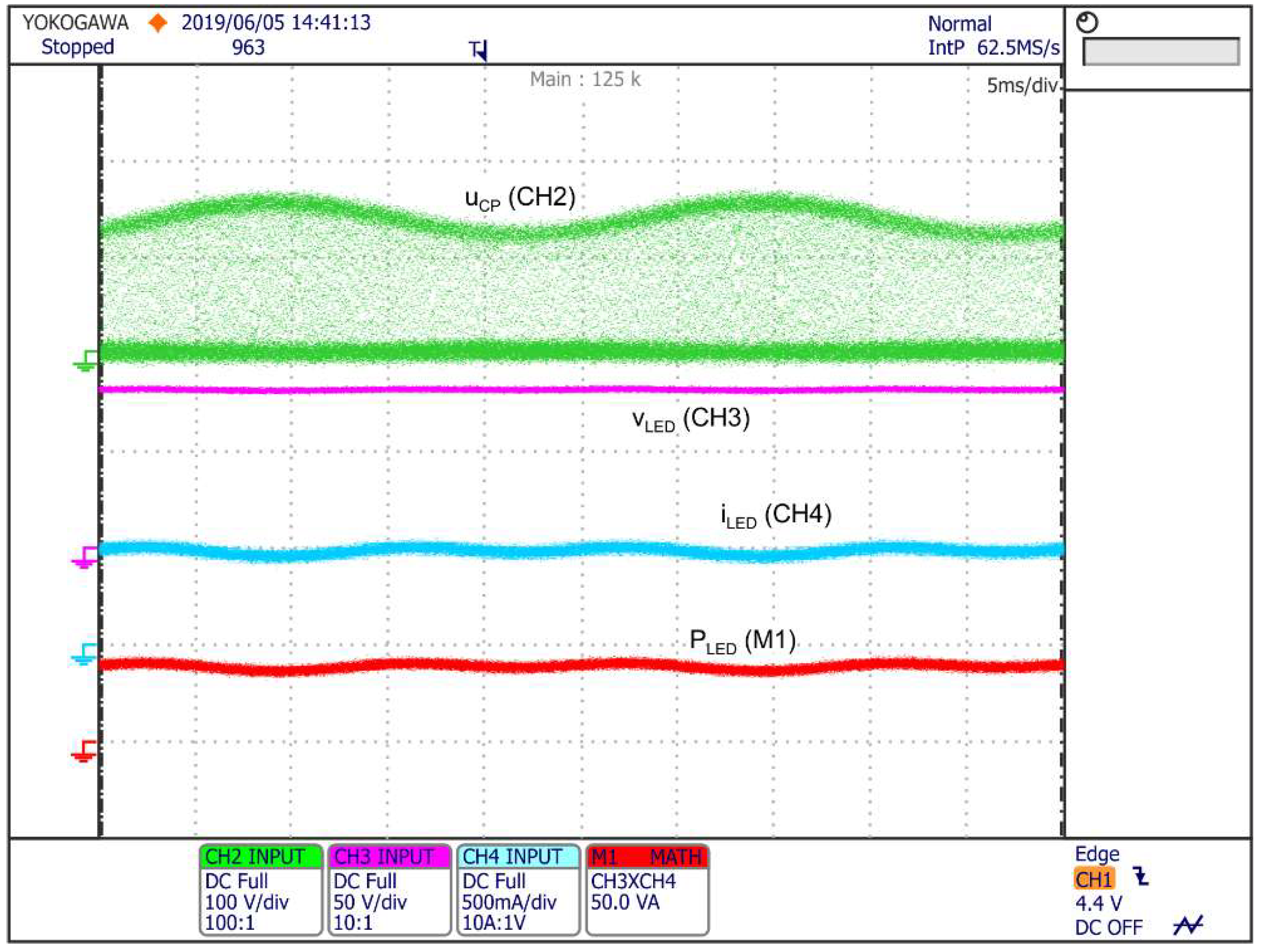
Figure 12. As it can be seen, the maximum efficiency is 95.7% at nominal power. One of the most interesting features observed is that the efficiency is kept above 90% even when the output power is dimmed below 25% of its nominal value. The minimum efficiency measured was 77.4% at 5% of the rated power.
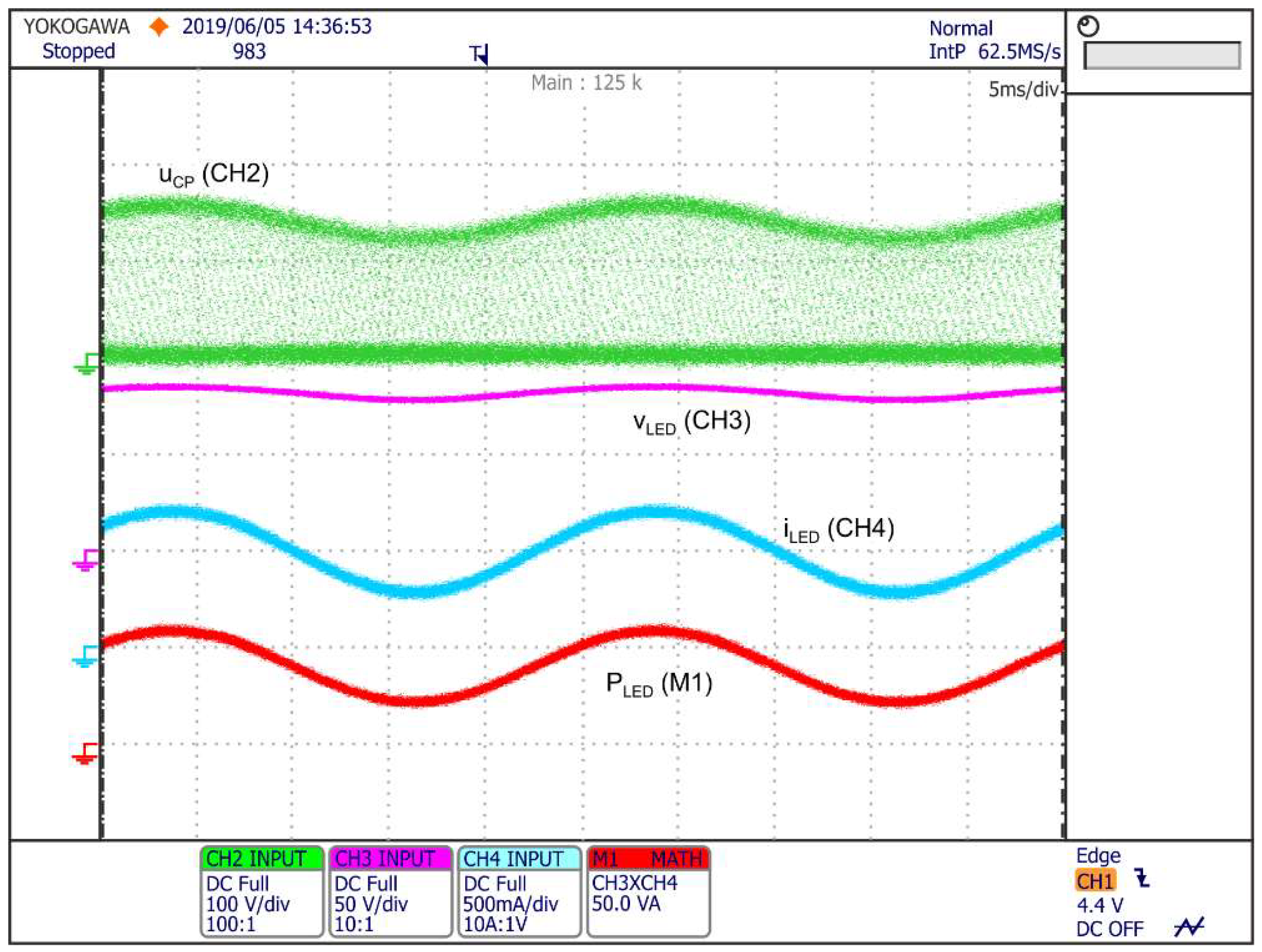
Figure 13 shows the lamp power and current at the nominal value of the bus voltage with a 100 Hz ripple of 16 V peak. This measurement was made at a constant switching frequency (i.e., with the feedforward control disabled). As it can be seen, there is a very high ripple in the lamp power thus the flicker recommendations of IEEE 1789 are not fulfilled.
Figure 14 shows the same waveforms as the previous figure but with the feedforward control enabled. As it can be observed, the lamp power flicker is highly reduced compared to the previous situation.
7. Conclusions
In present work, a new power topology based on a Class-E resonant inverter has been presented. The proposed topology works as a LED series current regulator and requires a single controlled switch referred to ground. As in the standard Class-E inverter, this converter is especially suited to operate at very high frequencies due to its extremely small switching losses.
The circuit behavior has been analyzed using the fundamental approach. This analysis has been oriented to obtain a set of charts that allow a straightforward design. Based on the proposed procedure, a design example has been carried out and the results obtained have been used to build a laboratory prototype.
A simple feedforward control has been used to compensate the variations in the bus and LED voltages. This control changed the switching frequency linearly with the difference between the bus and the lamp voltages. This allowed to compensate variations in both the input and LED voltages using a single voltage sensor. The prototype has been tested with a peak-to-peak input ripple up to 25% at 100 Hz without losing ZVS commutations.
The maximum efficiency measured was 95.7% at nominal power. One of the most interesting features observed during the experimentation is that the efficiency was kept above 90% even when the output power was dimmed below 25% of its nominal value.


