Article

Multiple Modulation Strategy of Flying Capacitor DC/DC Converter

by
Pengcheng Li
1,*,
Chunjiang Zhang
2,
Sanjeevikumar Padmanaban
3,* and
Leonowicz Zbigniew
4
1
Department of Electrical Engineering, Hebei University of Science and technology, Shijiazhuang 050018, China
2
Department of Electrical Engineering, Yanshan University, Qinhuangdao 066004, China
3
Department of Energy Technology, Aalborg University, 6700 Esbjerg, Denmark
4
Faculty of Electrical Engineering, Wroclaw University of Science and Technology, Wyb. Wyspianskiego 27, 50370 Wroclaw, Poland
*
Authors to whom correspondence should be addressed.
Electronics 2019, 8(7), 774; https://doi.org/10.3390/electronics8070774
Submission received: 24 May 2019 / Revised: 18 June 2019 / Accepted: 5 July 2019 / Published: 11 July 2019
(This article belongs to the Special Issue Power Converters in Power Electronics)

Abstract

:
Flying-capacitor multiplexed modulation technology is suitable for bipolar DC microgrids with higher voltage levels and higher current levels. The module combination and corresponding modulation method can be flexibly selected according to the voltage level and capacity level. This paper proposes a bipolar bidirectional DC/DC converter and its interleaved-complementary modulation strategy that is suitable for bipolar DC microgrids. The converter consists of two flying-capacitor three-level bidirectional DC/DC converters that are interleaved in parallel 90°, and then cascaded with another module to form a symmetrical structure of the upper and lower arms; the complementary modulation of the upper and lower half bridges constitutes an interleaved complementary multilevel bidirectional DC/DC converter. If the bidirectional converter needs to provide a stronger overcurrent capability, more bridge arms can be interleaved in parallel. Once n bridge arms are connected in parallel, the bridge arms should be interleaved 180°/n in parallel. In bipolar DC microgrids, the upper and lower arms should be complementarily modulated, and the input and output are isolated by the inductance. To solve the current difference, caused by the inconsistent parasitic, the voltage-current double closed-loop-control is used, and the dynamic response is faster during bidirectional operation. This paper proposes theoretical analysis and experiments that verify bipolar bidirectional DC/DC converter for high-power energy storage.

1. Introduction

With the high penetration of intermittent energy, such as solar and wind [1,2,3], a power electronic interface for distributed energy storage is becoming increasingly attractive. The bidirectional DC/DC converter (BDC) is an important piece of equipment for distributed energy storage in DC microgrids, which helps to promote intermittent energy scale applications. The BDCs are widely used in DC microgrids, due to their simple structure, easy expansion, and transmission power being independent of transformers [4,5,6,7].
In particular, it plays a large irreplaceable role in the distributed energy storage of high voltage and high power. For BDCs, current research focuses on buck/boost two-level converters and control strategies for suppressing load disturbances [8,9]; however, switches are subject to low-voltages applications. The voltage and current stresses of the converter are relatively high, so a multilevel converter is required. A multiplexed multiphase and multilevel BDC is used for a wide range of voltage variations (voltage conversion level less than 10 times); different from multilevel converters required for a high-voltage DC transmission (voltage conversion level more than 10 times), relying on transformer boosting to achieve a higher level of voltage conversion [10,11,12]. The n-level structure of the multiplexed multilevel BDC reduce voltage stress only 1/n of the high-side voltage; the m-phase of the multiplexed multiphase BDC reduce current stress only 1/m of the low-side current [13]. The multiphase and multilevel BDC adopts the interleaved phase modulation technology to improve the output current ripple frequency, reduce the filter capacitor ripple value in a DC microgrid [14,15,16,17].
When a battery is connected to a DC microgrid by a BDC, the BDC needs to have strong input and output impedance matching capability to keep the system stable. In particular, when the BDC operates in buck mode, the input impedance is large; when operating in boost mode, the input impedance is small; when operating in bidirectional mode, the impedance adjustment range is wider, and the response speed is faster, which is beneficial to the system stability [18].
H. L. Do. [19] proposed a soft-switching DC/DC converter with high voltage gain by a boost cell and a coupled inductor cell. Soft-switching characteristic reduces the switching loss of active power switches and increase the converter efficiency. However, the converter can only work in boost mode, and only S2 and D4 can achieve ZVS turn-on. The S1-D4 current stress is uneven, and S1 has a higher current stress. In high-voltage and high-power distributed energy storage, it is necessary to consider the equalization and current sharing problems. X. S. Zhang et al. [20] proposed the idea of battery energy storage systems (BESSs) with integrated wind farms to stabilize the grid power. High-power BDCs are required to meet high power requirements.
R. Naderi et al. [21] proposed a dual flying capacitor active-neutral-point-clamped (DFC-ANPC) DC/AC inverter with a five-level modulation method that achieves soft switching and neutral point voltage balancing. More importantly, the five-level modulation method eliminates the transient voltage balancing issue by series-connected switches of S5 and S6 and decreases the switching loss. F. Mohammadi [22] discussed the configuration, operation and decoupled control mode of a VSC-HVDC. Compared to the pulse width modulation (PWM) strategies, the vector control method generates fewer voltage harmonics and allows to control the active and reactive power independently. The vector control method is used to control the VSC-HVDC system, which is based on transforming a 3-φ system into a 2-φ system by d-q frame. Droop control is easily affected by the line impedance and the frequency fluctuation of the power grid, which reduces the distribution accuracy of the active and reactive power. In the future, the bidirectional DC/DC converter (BDC) will be connected to a bipolar DC microgrid by droop control.
Reference [23] used a DC bus capacitor to provide a three-level state (buck/boost synchronous PWM modulation). However, the converter operates at high gain, and S1 is subjected to high current stress, which exacerbates the switching losses. In Reference [24], a two-level buck/boost converter is cascaded to form a three-level bidirectional DC/DC converter. However, the modulation method easily causes inconsistent duty ratios of the upper and lower half bridges to be inconsistent, thereby affecting the voltage equalization effect of the DC bus, and requires an additional voltage equalization control loop at boost mode, which increases the complexity of the control structure.
This paper proposes a multiplexed modulation technique of the flying capacitor DC/DC converter to meet the high-voltage and high-power requirements. The BDC has many advantages: (1) the bus capacitor voltage is easily stabilized by the midpoint potential balance control of the rear inverter circuit; (2) the BDC is easy to combine by the PWM sequence to achieve multiple modulations; (3) it is easy to design the control loop and suppress phase-to-phase circulation; and (4) the BDC has a strong fault tolerance ability, and failure of any one of the arms does not affect the operation of other arms. The BDC is suitable for battery energy storage systems in bipolar DC microgrids.
This paper organized as follows. The Flying capacitor type three-level DC/DC basic unit in Section 2. Multiple modulation techniques are presented in Section 3. Controller design in Section 4. Experimental verifications in Section 5. Some conclusions are given in Section 6.

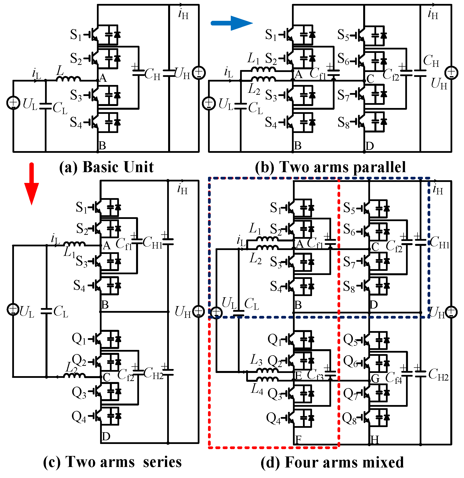
2. Flying Capacitor Type Three-level DC-DC Basic Unit

This paper proposes a bidirectional DC/DC converter (BDC) topology with multiplexed modulation strategy for a high-power system, as shown in Figure 1. The parallel operation improves the current capability of the BDC; the voltage level is increased in series operation; and the high-voltage and large-capacity characteristics are realized in series-parallel operation. The symbols and reference directions are indicated in the figure. The basic unit of the flying-capacitor-type three-level bidirectional DC/DC converter (3L_BDC) easily forms a bipolar BDC of high-voltage and high-current systems.
In Figure 1a, UL is the input-side voltage, UH is the DC bus side voltage, CL is the battery-side capacitance, and CH is the DC bus side capacitance. The conduction time of S3 and S4 is defined as Ton in the switching period Ts, and the duty ratio is D = Ton/Ts. To facilitate the analysis, define the switch function as follows:
M k = { 00 ( S 1 ,   S 2   ON ,    S 3 ,   S 4   OFF ) 01 ( S 2 ,   S 4   ON ,    S 1 ,   S 3   OFF ) 10 ( S 1 ,   S 3   ON ,    S 2 ,   S 4   OFF ) 11 ( S 3 ,   S 4   ON ,    S 1 ,   S 2   OFF ) .
The modal analysis is performed on the basic unit of the flying-capacitor-type three-level bidirectional DC/DC converter. The key waveform is shown in Figure 2. When the operating mode at D > 0.5, the switching mode of S3 and S4 is only 01, 10, 11, and not 00. The voltage at the two points of AB is 0.5UH or 0; at D < 0.5, the switching mode of S3 and S4 is only 00, 01, 10, and not 11. The voltage of AB is UH or 0.5UH. The inductive current flowing from the low-voltage side to the high-voltage side is defined as the positive direction.

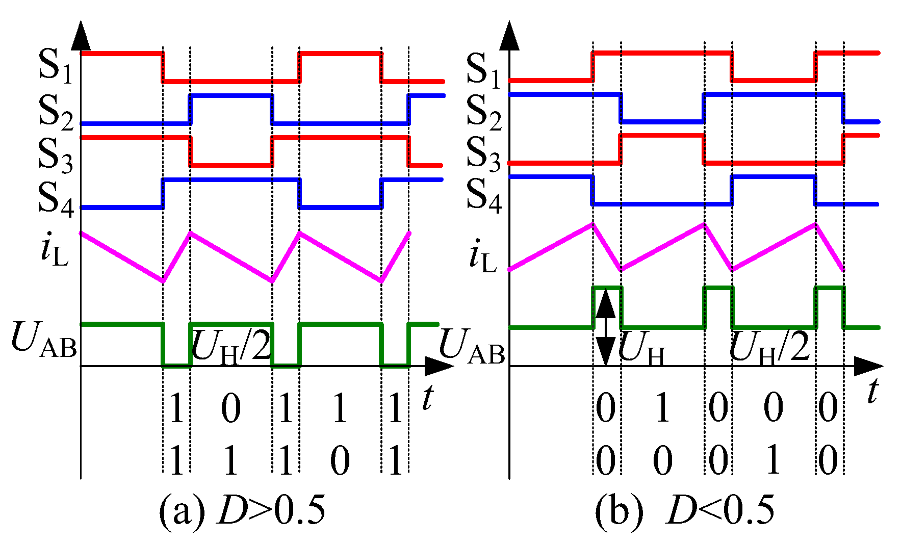
2.1. Operational Modal Analysis D > 0.5

During the switching cycle, there are three modes of 11, 01, and 10 for each arm.
  • Mode M3 = 11, S1 and S2 are turned off, S3 and S4 are turned on, S1 and S2 voltage stress are UH/2, the voltage of AB two-point is UAB = 0, the inductor voltage across L1 is UL, and iL flows to the high-voltage side and linearly increases:
    { i ˙ L = r L L i L + 1 L U L U ˙ H = 1 R H C H U H U ˙ f = 0 .
  • Mode M1 = 01, S1 and S3 turn off, S2 and S4 turn on, the S1 and S3 voltage stresses are UH/2, the flying capacitor Cf1 charge according to the differential equation Cf1 dUf1/dt = Ic, that is ΔUf1=t2Ic/Cf1 = Qc/Cf1, UAB = Uf1 = UH/2, the inductor L1 is UL - UAB < 0, the inductor current iL decreases linearly, and the average inductor current is IL = Ic.
    { i ˙ L = r L L i L + 1 L U L 1 L U f U ˙ H = 1 R H C H U H U ˙ f = 1 C f i L .
  • Mode M3 = 11, S1 and S2 are turned off, S3 and S4 are turned on, the S1 and S2 voltage stresses are UH/2, the voltage of the two-point of AB is UAB=0, the voltage of the inductance L1 is UL, and iL flows to high voltage side and linearly increase, as shown in Equation (2).
  • Mode M2 = 10, S2 and S4 are turned off, S1 and S3 are turned on, the S2 and S4 voltage stresses are UH/2, flying capacitor Cf1 is discharged, UAB = UHUf1 = UH/2, the voltage across inductor L1 is ULUAB < 0, and iL flows to the high-pressure side and decreases linearly. The column differential equation can be obtained as:
    { i ˙ L = r L L i L + 1 L U L + 1 L U f 1 L U H U ˙ H = 1 C H i L 1 R H C H U H U ˙ f = 1 C f i L .
According to the duty cycle definition, each equation group for the modal action time can be listed during the switching period:
{ t 1 + t 2 + t 3 = D T s t 1 + t 3 + t 4 = D T s t 1 + t 2 + t 3 + t 4 = T s { t 2 = ( 1 D ) T s    t 4 = ( 1 D ) T s    t 1 + t 3 = ( 2 D 1 ) T s .
The inductance satisfies the volt-second balance condition:
U L ( 2 D 1 ) T s + ( U L U H / 2 ) ( 2 2 D ) T s = 0 U H U L = 1 1 D .

2.2. Operational Modal Analysis D < 0.5

During the switching cycle, each arm has three modes of 00, 10, and 01.
  • Mode M0 = 00, S3 and S4 are turned off, S1 and S2 are turned on, the voltage of AB is UAB = UH, S3 and S4 voltage stress are UH/2, the voltage of inductance L1 is ULUH, iL flows to the high-voltage side and decreases linearly, and the corresponding differential equation can be expressed as:
    { i ˙ L = r L L i L + 1 L ( U L U H ) U ˙ H = 1 R H C H U H U ˙ f = 0 .
  • Mode M2 = 10, S2 and S4 are turned off, S1 and S3 are turned on, S2 and S4 voltage stress are UH/2, Cf1 is discharging, UAB = UHUf1 = UH/2, the voltage across inductor L1 is ULUAB>0, iL flows to the high-voltage side and increases linearly, and the differential equation can be expressed as Equation (4).
  • Mode M0 = 00, S3 and S4 are turned off, S1 and S2 are turned on, the voltage of AB is UAB = UH, S3 and S4 voltage stress are UH/2, inductance L1 voltage is ULUH, iL flow to high voltage side and the linearity is reduced, and the differential equation can be expressed as Equation (7).
  • Mode M1 = 01, S1 and S3 are turned off, S2 and S4 are turned on, S1 and S3 voltage stresses are UH/2, flying capacitor Cf1 is charging, UAB = Uf1 = UH/2, the inductor voltage across L1 is ULUAB > 0, iL flows to the high-voltage side and increases linearly, and the differential equation can be expressed as Equation (3). According to the duty cycle definition, each mode action time can be expressed as:
    { t 2 = D T s t 4 = D T s t 1 + t 3 = ( 1 2 D ) T s .
The inductance satisfies the volt-second balance:
2 D T s ( U L U H / 2 ) + ( 1 2 D ) T s ( U L U H ) = 0 U H U L = 1 1 D .

3. Multiple Modulation Technique

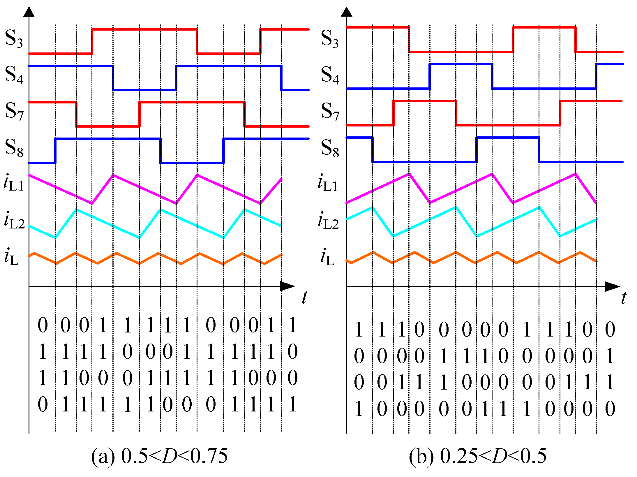
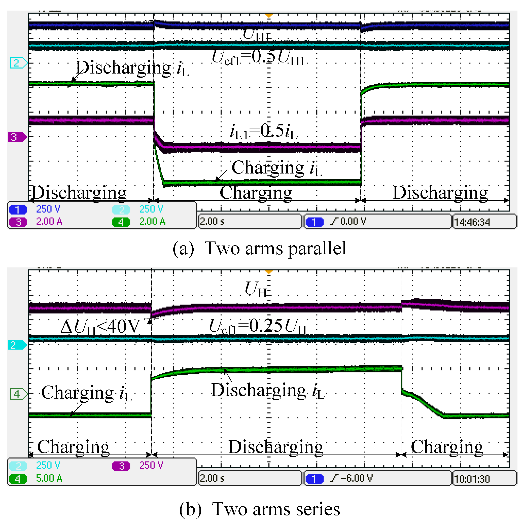
3.1. Two Arms Interleaved Parallel Modulation

Two arms are paralleled, as shown in in Figure 1b, to increase the overcurrent capability and reduce the input side ripple. Arm 1 is composed of S1-S4, the inductor L1 and the flying capacitor Cf1; and arm 2 is composed of S5, S6, S7, S8, the inductor L2 and the flying capacitor Cf2. Among them, S1 and S4 are turned on complementarily, S2 and S3 are turned on complementarily, the modulated waves of S1 and S2 are interleaved 180°, and the S3 and S4 modulated waves are interleaved 180°, as shown in Figure 3. Arm 2 is modulated in the same manner as arm 1 with a phase lag of 90°.
Two arms are interleaved 90° in parallel; eight modes are used at 0.5 < D < 0.75, and other eight modes are used at 0.25 < D < 0.5. The working mode of the space ratio is shown in Table 1. In the forward power flow (Boost mode), the inductor currents iL1 and iL2 are positive and flow from the low voltage side to the high voltage side. When the negative power flows (Buck mode), the inductor currents of iL1 and iL2 are negative, and the high voltage side flows to the low voltage side. The driving signal between the two arms is interleaved 90°, and the other side bridge arm switch maintains the original state when one side bridge arm is operated. After the inductor current is superimposed, the low-voltage side current is iL = iL1 + iL2 doubling the pulsation frequency, and the ripple of the iL is reduced.
Then the inductor current is superimposed, the low-voltage side current is iL = iL1 + iL2 doubling the pulsation frequency, and the ripple of the iL is reduced. According to Equations (2)–(9), the ripple current of three-level bi-directional DC/DC(3L-BDC) in Figure 1b, ΔIL1_3L_LBDC, can be calculated as
Δ I L 1 _ 3 L _ BDC = { ( U H 2 U L ) ( 1 D ) 2 L 1 f s , ( D > 0.5 ) ( 2 U L U H ) D 2 L 1 f s , ( D 0.5 ) .
Correspondingly, the ripple current of the inductor of two-level bidirectional DC/DC (2L_ BDC) can be calculated as
Δ I L 1 _ 2 L _ BDC = ( U H U L ) D L 1 f s .
To reduce currents ripple, n arms can be cascaded, and the drive signals between the arms are interleaved 180°/n. The more arms that participate in interleaved parallel connection, the more obvious the ripple reduction effect, and the more characteristic points of zero ripple appear at the same time—these zero ripple points show a uniform distribution law. The aforementioned analysis shows that the voltage stress on the switches and the flying capacitors of the 3L_BDC is half of UH, which is just half of the traditional 2L_BDC. To reduce the voltage stress, it is necessary to employ a series connection.

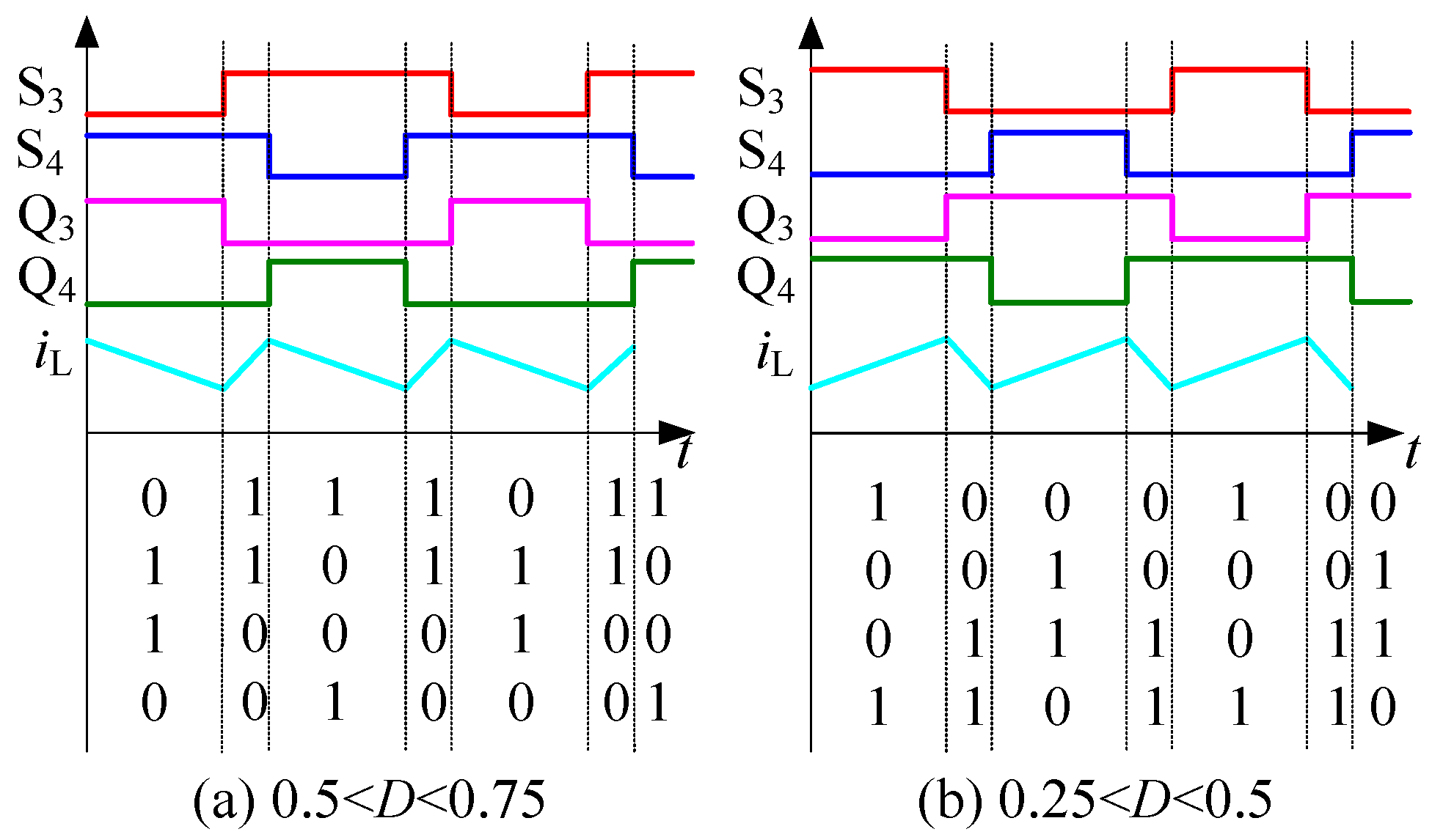
3.2. Two Arms Complementary Series Modulation

The topology is connected in series with two inductors to reduce the inductor current ripple amplitude; the low voltage side is isolated from the output side by two inductors, which can improve the energy storage unit safety; the series structure can reduce the voltage stress of the switches and increase the voltage level of the DBC, as shown in Figure 1c. The inductor current waveform during complementary modulation is shown in Figure 4. S4 and Q1 are the same drive signal, S3 and Q2 are the same drive signal, S2 and Q3 are the same drive signal, and S1 and Q4 are the same drive signal; that is, the switch modulation is based on the topology. The switching period inductance fluctuation frequency is equal to twice of the switching frequency, the inductance fluctuation amplitude is half of that of the single submodule, and the remaining mode complementary series modulation is shown in Table 2.
The voltage stress on the switches and the flying capacitors is 0.25 UH in Figure 1c. In order to reduce the voltage and current stress, it is necessary to increase the series and parallel bridge arms simultaneously. The ripple current of L1 in Figure 1c, ΔIL1_3L_LBDC, can be calculated as
Δ I L 1 _ 3 L _ BDC = { ( U H 2 U L ) ( 1 D ) 2 ( L 1 + L 3 ) f s , ( D > 0.5 ) ( 2 U L U H ) D 2 ( L 1 + L 3 ) f s , ( D 0.5 ) .

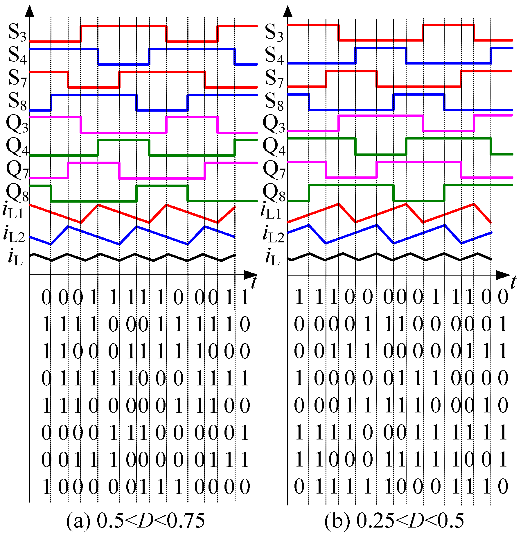
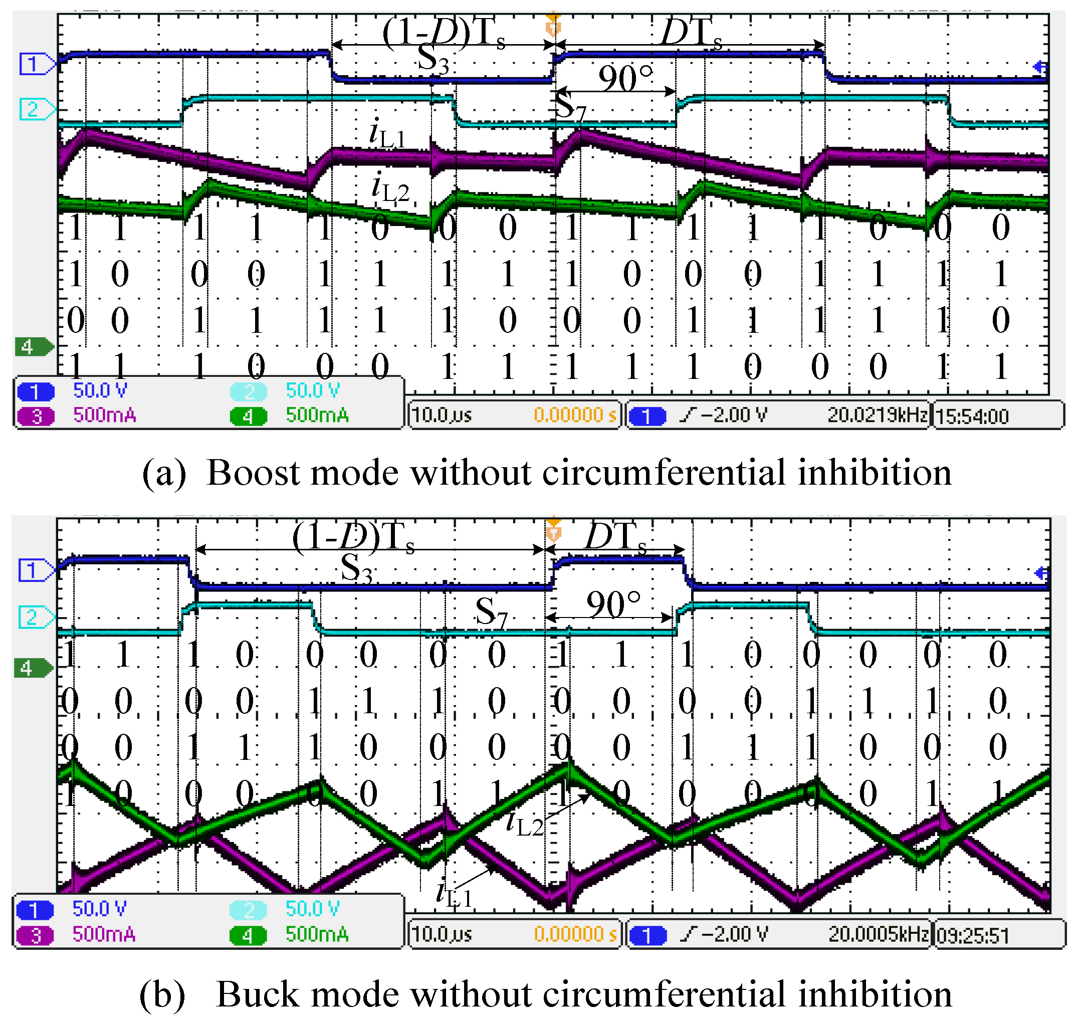
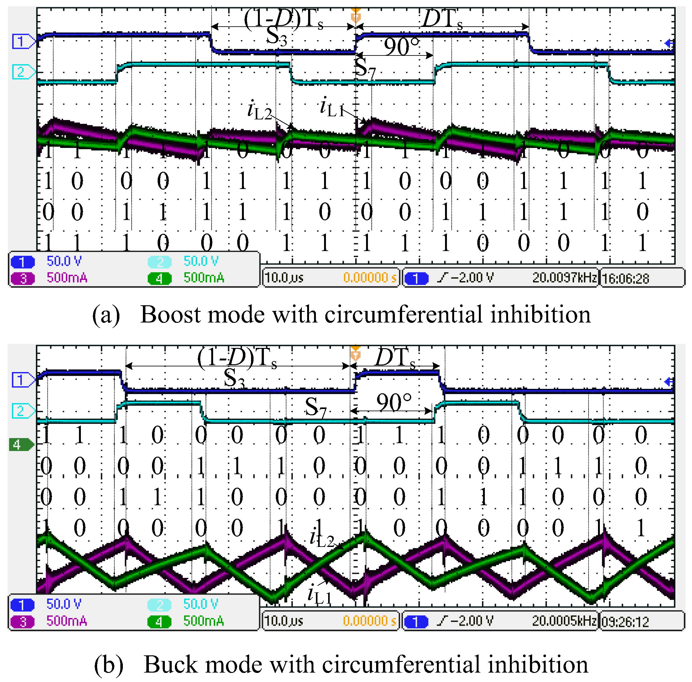
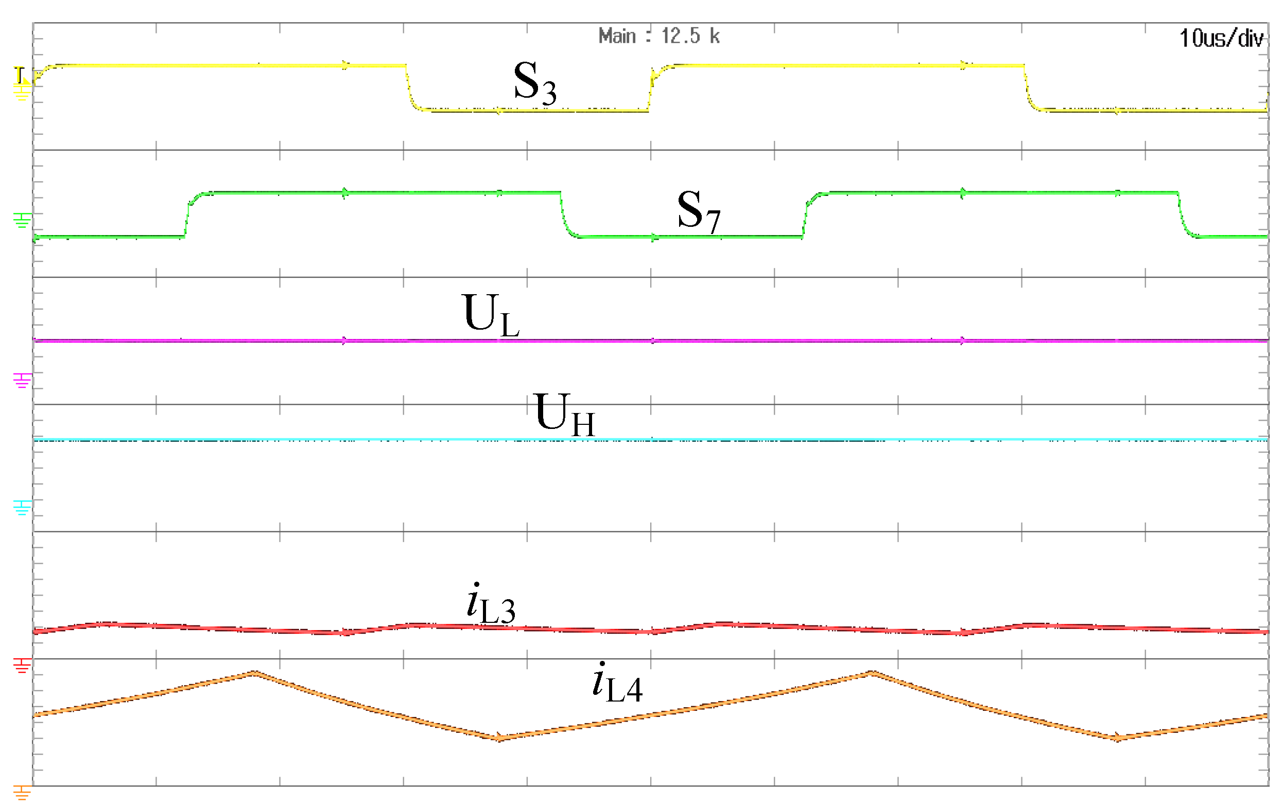
3.3. Four Arms Mixed Modulation

To meet the large-capacity requirements in the bipolar DC bus, the voltage and current stress of the switching tube should be reduced, so a four-arms mixed converter is proposed, that is, the cascaded form of the interleaved parallel flying-capacitor type three-level converter, as shown in Figure 1d. The left and right parallel arms are interleaved 90° parallel modulation, and the upper and lower series arms are complementarily connected in series. For example, when 0.5 < D < 0.75, in mode 0101/1010, it means S3 is off, S4 is on, S7 is off, S8 is on; while, Q3 is on, Q4 is off, Q7 is on, and Q8 is off. The modulation rule of the BDC is shown in Figure 5.
By mixed modulation, the average inductor current is only half of the single-arm current, the ripple frequency is doubled, the flying capacitor voltage is 0.25 UH, and the voltage stress of the switch is only 0.25 UH compared to the 2L_BDC. The modulation is shown in Table 3. To compare the characteristics of the structure, shown in Figure 1, the voltage and current stress conditions are listed in Table 3, and the four arms mixed modulation is more suitable for bipolar high-power applications. This modulation strategy helps to control and protect the design of the circuit. A topological comparison of the proposed BDC in this paper with others are shown in Table 4.

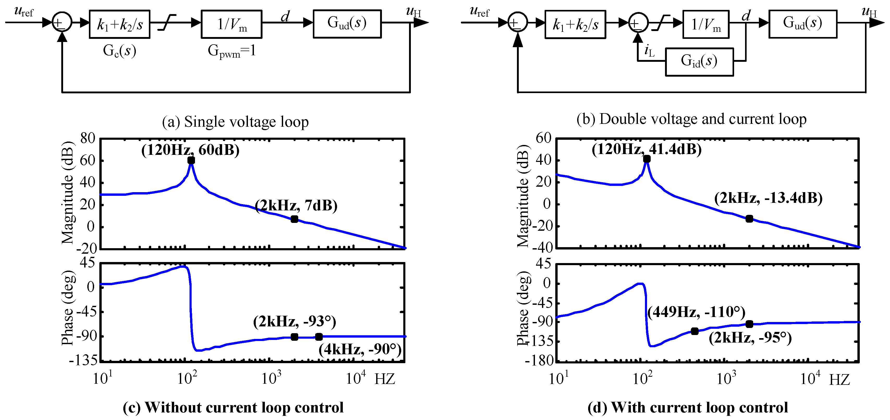
4. Controller design

Define the state variable as x = [ iL, UH, Uf ]T, the input variable as u = UL, the transfer function as Gid(s) from the duty cycle d to the inductor current iL and the transfer function Gud(s) from the duty cycle d to the output voltage UH, according to Equations (2)–(9).
G id ( s ) = U L C H R H 1 D s + 2 U L 1 D C H L R H s 2 + L s + R H ( 1 D ) 2 + r L ,
G ud ( s ) = L U L ( 1 D ) 2 s + R H U L r L U L ( 1 D ) 2 C H L R H s 2 + L s + R H ( 1 D ) 2 + r L ,
where, RH is Rload, and rL is the inductance parasitic resistance.
The main circuit parameters of the converter are shown in Table 5. Due to the inconsistent impedance of the IGBT parasitic parameters and the inductor winding process, the main loop has a certain degree of impedance difference. The controller’s PI regulator is Gc(s) = k1 + k2/s, where k1 = 0.1, k2 = 50, and the control block diagram is shown in Figure 6.
The Bode diagram of the proposed control strategy by a single voltage loop, as shown in Figure 6c. The low frequency range is 30 dB, the high frequency band traverses 0 dB with a slope of −20 dB/dec, and the corner frequency is 120 Hz. The gain crossover frequency is 4 kHz, the phase margin is 90°, and the system is stable; however, the gain is higher than 0dB at 0.1 times of switching frequency. The current inner loop uses inductor current feedback, as shown in Figure 6d. The PI regulator is Gc(s) = 0.1 + 50/s, the crossing frequency of the open-loop transfer function is 449 Hz when crossing the 0 dB line, and the phase margin is 70° at the crossing frequency. It can be judged that the closed loop system is stable. A first-order low-pass filter is added to the loop due to the influence of high frequency noise. The cutoff frequency of the first-order low-pass filter (ωc = 2πfc) is set at 0.1 times the switching frequency, and the gain margin kg (fc = 2 kHz) is 13.4 dB, which is ideal. The pole introduced by the first-order LPF is far from the real axis, and has little effect on the bode diagram and can be ignored.

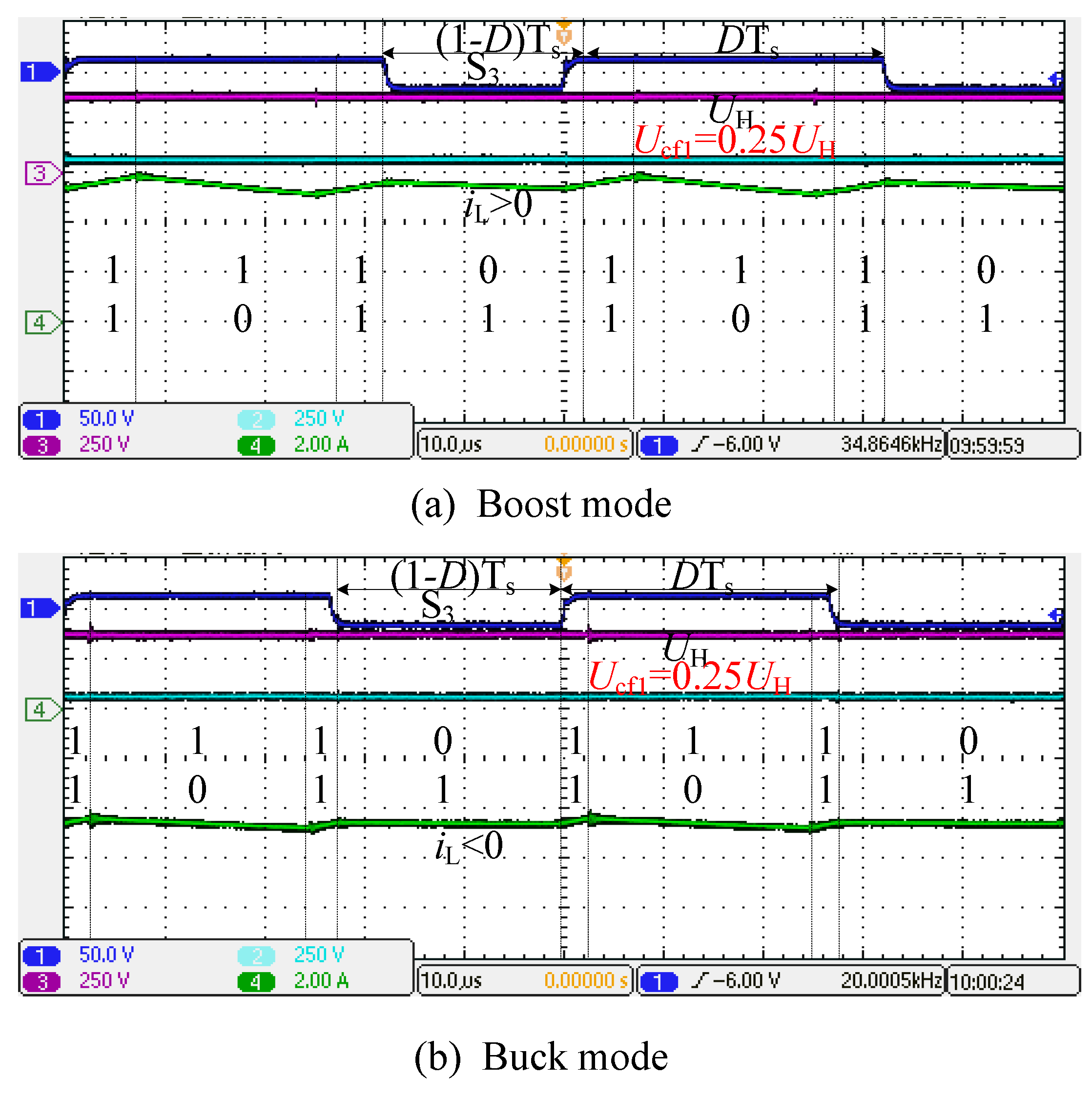
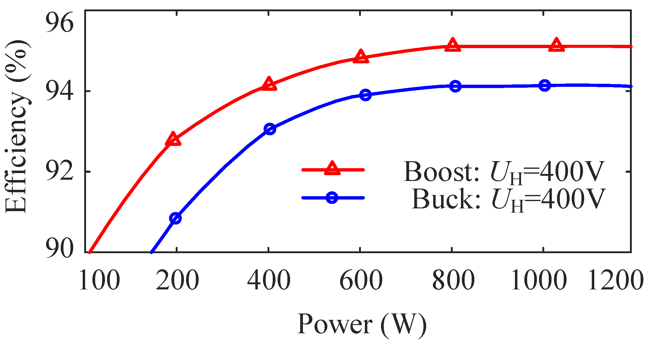
5. Experimental result

The experimental platform is shown in Figure 7. In the platform, the DC power supply E and resistance R are used to simulate the power generation change of the renewable energy source. The rated voltage of the DC power supply E is 450 V, and the DC bus voltage rating is 400 V. Super capacitor rated voltage is 250 V, rated capacity is 10 F, maximum discharge current is 15 A, charging current is 10 A, super capacitor voltage UL range is 150~220 V; switching frequency fs is 20 kHz. DC power supply Chroma 62050H-600 (Chroma Systems Solutions, Inc., Foothill Ranch, CA, USA), DC probe YOKOGAWA 701934 (Yokogawa Electric, Inc., Tokyo, Japan), oscilloscope Tek DPO2024B (Tektronix, Inc., Beaverton, OR, USA). The control chip uses DSP (TMS28335) combined with FPGA (EP3C25Q240); DSP is used for signal sampling and control signal generation, and FPGA is used to generate the modulated wave. To test the feasibility of multiple applications, super capacitor UL = 200V, high side load RH = 200 Ω, adjustable power supply E = 450 V, resistance R = 10 Ω; during switch S disconnection, super capacitor discharge, converter operates on boost 0.5 < D < 0.75 mode, the high side capacitor voltage is stable to UH = 400 V. Super capacitor UL = 250 V, high-voltage-side load RH = 200 Ω, adjustable power supply E = 450 V, resistance R = 10 Ω; during switch S closing, super capacitor charging.
In the project, due to the inconsistent IGBT parasitic parameters and the inconsistent impedance caused by the inductor winding process, the main loop objectively has impedance differences.
The voltage and current double closed-loop PI regulators are used for impedance matching. The two control loops share the voltage outer loop, and the current inner loop uses respective inductor current feedback. The control loop is shown in Figure 7b. The difference in the modulation signals generated by the control loop adjusts the respective output impedances to achieve current sharing control. The left and right arms are interleaved 90° parallel, the two inductor current ripples cancel each other, and the output voltage is stable, as shown in Figure 8 and Figure 9. The current iL fluctuating frequency is twice of the switching frequency, and the inductor current fluctuation amplitude is reduced, due to iL through two inductors evenly. Two arms series, the flying capacitor voltage is 0.25 UH, as shown in Figure 10. The inductor current ripple is small, and the flying capacitor voltage is equal to 0.25 UH.
Switch S is turned on at tON, and the supercapacitor charging power is 800 W in buck mode. Switch S is turned off at tOFF, and the supercapacitor discharging power is 1200 W in boost mode, as shown in Figure 11. The dynamic response time is less than 20 ms from charging to discharging. The dynamic response time is 400 ms from discharging to charging in the four-arms mixed modes. The flying capacitor voltage is always stable, and the DC bus voltage fluctuation is less than 20 V. The input voltage varies between 150–220 V, the output voltage is stable at 400 V, and the change range of D is 0.63–0.45. From the experimental results in Figure 8, Figure 9, Figure 10 and Figure 11, it can be seen that the input and output side voltage ripple is less than 1%, and the current ripple frequency is relatively small, which is beneficial to the stable operation of the energy storage unit. When Q7 shorted, iL4 ripple is only once per cycle, losing the advantage of three levels. However, the overall performance of the converter remains stable, and the input and output voltage ripples are low, as shown in Figure 12. Therefore, the BDC has a strong fault tolerance ability, and failure of any one of the arms does not affect the operation of other arms.
The efficiency is reduced, due to the inherent loss increase with a light load. Since there is a dead time of 1.5 µs when the converter is actually running, energy can be transferred from the low voltage side to the high voltage side through the IGBT body diode during dead time, as shown in Figure 13. Thus, the boost mode efficiency is higher than the buck mode. The efficiency curve is more than 90% from light load to heavy load, meeting design requirements.

6. Conclusions

This paper proposes a BDC topology with a multiplexed modulation strategy for high-power energy storage in bipolar DC microgrids. The parallel arms divide the input side current, which can effectively overcome the current difference caused by the inconsistent parasitic parameters of the parallel arms. The series arms divide the voltage of the high voltage side, which can effectively reduce the voltage stress of the switch and the flying capacitor. The bidirectional transient response is milliseconds, which ensures the dynamic performance and operating efficiency of the converter. The BDC has a strong fault tolerance ability, and the failure of any one of the arms does not affect the operation of other arms. The proposed BDC topology and its modulation strategy can effectively solve the issue of high-power energy storage in bipolar DC microgrids.

Author Contributions

P.L. designed the prototype and was responsible for writing the paper. C.Z., S.P. and L.Z. were responsible for guidance in the experiment and thesis writing process.

Funding

This research was supported by the National Nature Science Foundation of China under Grants 51477148 and the Science Foundation of Hebei University of Science and technology Grants PYB2019011. This research also received funding from EEEIC International, Poland.

Conflicts of Interest

The authors declare no potential conflict of interest.

References

  1. Ji, Y.; Yang, Y.; Zhou, J.; Ding, H.; Guo, X.; Padmanaban, S. Control Strategies of Mitigating Dead-time Effect on Power Converters: An Overview. Electronics 2019, 8, 196. [Google Scholar] [CrossRef]
  2. Guo, X.; Jia, X. Hardware-based cascaded topology and modulation strategy with leakage current reduction for transformerless PV systems. IEEE Trans. Ind. Electron. 2016, 62, 7823–7832. [Google Scholar] [CrossRef]
  3. Guo, X.; Yang, R.Y.; He, R.; Wang, B.; Blaabjerg, F. Transformerless Z-source four-leg PV inverter with leakage current reduction. IEEE Trans. Power Electron. 2019, 34, 4343–4352. [Google Scholar] [CrossRef]
  4. Mahmoudi, M.A.H.; Ahmadi, R. Modulated model predictive control of three level flying capacitor buck converter. In Proceedings of the IEEE Power and Energy Conference at Illinois (PECI), Champaign, IL USA, 23–24 February 2017; pp. 1–5. [Google Scholar]
  5. Jin, K.; Yang, M.; Ruan, X.; Xu, M. Three-Level Bidirectional Converter for Fuel-Cell/Battery Hybrid Power System. IEEE Trans. Ind. Electron. 2010, 57, 1976–1986. [Google Scholar] [CrossRef]
  6. Zhang, C.; Li, P.; Kan, Z.; Chai, X.; Guo, X. Integrated Half Bridge CLLC Bidirectional Converter for Energy Storage Systems. IEEE Trans. Ind. Electron. 2018, 65, 3879–3889. [Google Scholar] [CrossRef]
  7. Li, P.; Zhang, C.; Kan, Z.; Fu, Y. An Interleaving 90° Three-Level DC-DC Converter and Current Sharing Control. In Proceedings of the 2nd IEEE International Power Electronics and Application Conference and Exposition, Shenzhen, China, 4–7 November 2018. [Google Scholar]
  8. Dragičević, T.; Guerrero, J.M.; Vasquez, J.C.; Škrlec, D. Supervisory Control of an Adaptive-Droop Regulated DC Microgrid with Battery Management Capability. IEEE Trans. Power Electron. 2014, 29, 695–706. [Google Scholar] [CrossRef]
  9. Huang, X.; Lee, F.C.; Li, Q.; Du, W. High-Frequency High-Efficiency GaN-Based Interleaved CRM Bidirectional Buck/Boost Converter with Inverse Coupled Inductor. IEEE Trans. Power Electron. 2016, 31, 4343–4352. [Google Scholar] [CrossRef]
  10. Xiao, G.; Zhou, J.; He, R.; Jia, X.; Rojas, C.A. Leakage current attenuation of a three-phase cascaded inverter for transformerless grid-connected pv systems. IEEE Trans. Ind. Electron. 2018, 65, 676–686. [Google Scholar]
  11. Chen, W.; Ruan, X.; Yan, H.; Tse, C.K. DC/DC Conversion Systems Consisting of Multiple Converter Modules: Stability, Control, and Experimental Verifications. IEEE Trans. Power Electron. 2009, 24, 1463–1474. [Google Scholar] [CrossRef]
  12. Jin, L.; Liu, B.Y.; Duan, S.X. ZVS Operation Range Analysis of Three-Level Dual Active Bridge DC-DC Converter with Phase-Shift Control. In Proceedings of the 2017 Thirty Second Annual IEEE Applied Power Electronics Conference and Exposition (Apec), Tampa, FL, USA, 26–30 March 2017. [Google Scholar]
  13. Wang, Y.; Yuan, Z.; Fu, J.; Li, Y.; Zhao, Y. A feasible coordination protection strategy for MMC-MTDC systems under DC faults. Int. J. Electr. Power Energy Syst. 2017, 90, 103–111. [Google Scholar] [CrossRef]
  14. Kakigano, H.; Miura, Y.; Ise, T. Low-Voltage Bipolar-Type DC Microgrid for Super High-Quality Distribution. IEEE Trans. Power Electron. 2010, 25, 3066–3075. [Google Scholar] [CrossRef]
  15. Xiao, G.; Yang, Y.; Wang, B.; Blaabjerg, F. Leakage Current Reduction of Three-phase Z-source three-level four-leg inverter for transformerless PV system. IEEE Trans. Power Electron. 2019, 34, 6299–6308. [Google Scholar]
  16. Dusmez, S.; Khaligh, A.; Hasanzadeh, A. A Zero-Voltage-Transition Bidirectional DC/DC Converter. IEEE Trans. Ind. Electron. 2015, 62, 3152–3162. [Google Scholar] [CrossRef]
  17. Guo, Z.; Chai, X.; Li, P.; Zhang, C. A new balance control method of three-level converter NPP. In Proceedings of the IEEE 8th International Power Electronics and Motion Control Conference (IPEMC-ECCE Asia), Piscataway, NJ, USA, 22–26 May 2016; pp. 2356–2361. [Google Scholar]
  18. Singh, S.N. Selection of non-isolated DC-DC converters for solar photovoltaic system. Renew. Sustain. Energy Rev. 2017, 76, 1230–1247. [Google Scholar]
  19. Do, H.L. A Soft-Switching DC/DC Converter with High Voltage Gain. IEEE Trans. Power Electron. 2010, 25, 1193–1200. [Google Scholar]
  20. Zhang, X.S.; Yuan, Y.; Hua, L.; Cao, Y.; Qian, K.J. On Generation Schedule Tracking of Wind Farms with Battery Energy Storage Systems. IEEE Trans. Sustain. Energy 2017, 8, 341–353. [Google Scholar] [CrossRef]
  21. Naderi, R.; Sadigh, A.K.; Smedley, K.M. Dual Flying Capacitor Active-Neutral-Point-Clamped Multilevel Converter. IEEE Trans. Power Electron. 2016, 31, 6476–6484. [Google Scholar] [CrossRef]
  22. Mohammadi, F. Power Management Strategy in Multi-Terminal VSC-HVDC System. In Proceedings of the 4th National Conference on Applied Research in Electrical, Mechanical, Computer and IT Engineering, Tehran, Iran, 5 January 2018. [Google Scholar]
  23. Uno, M. High Step-Down Converter Integrating Switched Capacitor Converter and PWM Synchronous Buck Converter. In Proceedings of the 35th International Telecommunications Energy Conference, Hamburg, Germany, 13–17 October 2013. [Google Scholar]
  24. Li, X.; Zhang, W.; Li, H.; Xie, R.; Xu, D. Design and control of bi-directional DC/DC converter for 30kW fuel cell power system. In Proceedings of the 8th International Conference on Power Electronics-ECCE Asia, Jeju, Korea, 30 May–3 June 2011; pp. 1024–1030. [Google Scholar]
Figure 1. The proposed bidirectional DC/DC converter. (a) Flying capacitor type three-level DC-DC basic unit. (b) Two basic units parallel. (c) Two basic units parallel. (d) Four basic units mixed.
Electronics 08 00774 g001
Figure 2. The main waveform of the basic unit. (a) Mode D > 0.5. (b) Mode D < 0.5.
Electronics 08 00774 g002
Figure 3. The main waveform of two parallel arms. (a) Mode 0.5 < D < 0.75, (b) Mode 0.25 < D < 0.5.
Electronics 08 00774 g003
Figure 4. The key waveform of two arms series. (a) Mode 0.5 < D < 0.75, (b) Mode 0.25 < D < 0.5.
Electronics 08 00774 g004
Figure 5. The key waveform of the four arms mixed. (a) Mode 0.5 < D < 0.75, (b) Mode 0.25 < D < 0.5.
Electronics 08 00774 g005
Figure 6. The control strategy. (a) & (c) are single voltage loop and its Bode without current loop control. (b) & (d) are double voltage-current loop and its Bode with current loop control.
Electronics 08 00774 g006
Figure 7. Experimental setup. (a) The experimental system, (b) Control system logic.
Electronics 08 00774 g007
Figure 8. Left and right arms interleaved 90º parallel without circumferential inhibition. (a) Boost mode. (b) Buck mode.
Electronics 08 00774 g008
Figure 9. Left and right arms interleaved 90º parallel with circumferential inhibition. (a) Boost mode, (b) Buck mode.
Electronics 08 00774 g009
Figure 10. Two arms complementary series. (a) Boost mode, (b) Buck mode.
Electronics 08 00774 g010
Figure 11. Transient response for bidirectional operation. (a) Two arms interleaved parallel transient response, (b) Two arms complementary series transient response.
Electronics 08 00774 g011
Figure 12. Switch Q7 short circuit experiment.
Electronics 08 00774 g012
Figure 13. The efficiency curves.
Electronics 08 00774 g013
Table 1. Two arms interleaved parallel coding.
0~0.25D = 0.250.25~0.5D = 0.50.5~0.75D = 0.750.75~1
0000001010101010010111011111
0010001000101010110111011101
0000010001100110100110111111
0100010001000110101110111011
0000000101010101101011101111
0001000100010101111011101110
0000100010011001011001111111
1000100010001001011101110111
Table 2. Two arms complementary series coding.
0~0.250.250.25~0.50.50.5~0.750.750.75~1
00/1100/1100/1101/1011/0011/0011/00
01/1001/1001/1010/0110/0110/0110/01
00/1100/1100/1101/1011/0011/0011/00
10/0110/0110/0110/0101/1001/1001/10
Table 3. Four arms mixed modulation coding.
0~0.25D = 0.250.25~0.5D = 0.50.5~0.75D = 0.750.75~1
0000/11110010/11011010/01011010/01010101/10101101/00101111/0000
0010/11010010/11010010/11011010/01011101/00101101/00101101/0010
0000/11110100/10110110/10010110/10011001/01101011/01001111/0000
0100/10110100/10110100/10110110/10011011/01001011/01001011/0100
0000/11110001/11100101/10100101/10101010/01011110/00011111/0000
0001/11100001/11100001/11100101/10101110/00011110/00011110/0001
0000/11111000/01111001/01101001/01100110/10010111/10001111/0000
1000/01111000/01111000/01111001/01100111/10000111/10000111/1000
Table 4. Topological comparison.
(a) Comparison in terms of passive component and out gain, inductor ripple current and switching frequency.
ProposedNumber of ElementsGain of VoltageΔiL f Δ i L
SC [23]C = 3 S = 4 L = 1 2 U L 1 D ( U H 2 U L ) D 2 L f s fs
Double Buck/Boost [24]C = 3 S = 4 L = 2 U L 1 D U H ( 1 D ) D L f s 2fs
Basic FC [5]C = 3 S = 4 L = 1 U L 1 D { ( U H 2 U L ) ( 1 D ) 2 L 1 f s , ( D > 0.5 ) ( 2 U L U H ) D 2 L 1 f s , ( D 0.5 ) 2fs
Interleaved FC [7]C = 4 S = 8 L = 2 U L 1 D { ( U H 2 U L ) ( 1 D ) 2 L 1 f s , ( D > 0.5 ) ( 2 U L U H ) D 2 L 1 f s , ( D 0.5 ) 4fs
Complementary FC [21]C = 5 S = 8 L = 2 U L 1 D { ( U H 2 U L ) ( 1 D ) 2 ( L 1 + L 3 ) f s , ( D > 0.5 ) ( 2 U L U H ) D 2 ( L 1 + L 3 ) f s , ( D 0.5 ) 2fs
This paperC = 7 S = 16 L = 4 U L 1 D { ( U H 2 U L ) ( 1 D ) 2 ( L 1 + L 3 ) f s , ( D > 0.5 ) ( 2 U L U H ) D 2 ( L 1 + L 3 ) f s , ( D 0.5 ) 4fs
(b) Comparison in terms of out capacitor, flying capacitor voltage, voltage across switch, inductor current and fault tolerant capabilities
Proposed.Output Capacitor VoltageFlying capacitor voltageSwitch VoltageInductor CurrentFault Tolerance
SC [23]2 UL/(1-D)0.5 UH0.5 UHILWeak
Double Buck/Boost [24]UL/(1-D)No0.5 UHILWeak
Basic FC [5]UL/(1-D)0.5 UH0.5 UHILWeak
Interleaved FC [7]UL/(1-D)0.5 UH0.5 UH0.5 ILAverage
Complementary FC [21]UL/(2-2D)0.25 UH0.25 UHILAverage
This paperUL/(2-2D)0.25 UH0.25 UH0.5 ILStrong
Table 5. The Parameters of BDC.
ParametersValueParametersValue
UL/V150~220CL/μF220
UH/V400CH/μF110
Po/kW1Cf1/μF110
L1~L2/mH2Cf2/μF110
rL0.2fs/kHz20

