Article

Miniature Compact Folded Dipole for Metal Mountable UHF RFID Tag Antenna

1
Department of Electrical Engineering, University of Malaya, 50603 Kuala Lumpur, Malaysia
2
Department of Electrical and Electronic Engineering, Universiti Tunku Abdul Rahman, 43000 Selangor, Malaysia
3
Complex of Science and Technology, Faculty of Science and Natural Resources, Universiti Malaysia Sabah, 88400 Kota Kinabalu, Malaysia
*
Authors to whom correspondence should be addressed.
Electronics 2019, 8(6), 713; https://doi.org/10.3390/electronics8060713
Submission received: 10 May 2019 / Revised: 14 June 2019 / Accepted: 19 June 2019 / Published: 24 June 2019
(This article belongs to the Special Issue Advanced RFID Technology and Applications)

Abstract

:
This article describes the design of an Ultra-High Frequency (UHF) miniature folded dipole Radio Frequency Identification (RFID) tag antenna that can be mountable on metallic objects. The compact tag antenna is formed from symmetric C-shaped resonators connected with additional arms embedded into the outer strip lines for miniaturization purposes. It is loaded with outer strip lines, resulting in a flexible tuning method that is capable of matching the integrated circuit (IC) chip’s impedance. The proposed tag is fabricated on a single layer of Polytetrafluoroethylene (PTFE) substrate. It has simple structure and does not require any metallic vias or shorting plate. The miniature tag antenna with a size of 82.75 × 19.5 × 1.5   mm 3 yields a total realized gain of 0.53   dB at the resonance frequency when attached to a 40 × 40   cm 2 metal plate. The presented design utilizes a European RFID band, and the simulated results of realized gain, read range, and input impedance are verified with measurement results.

1. Introduction

Recently, the implementation of a passive radio frequency identification (RFID) ( 860 960   MHz ) has attracted a considerable amount of attention from numerous sectors, such as logistics, retail industries, and tracking management [1,2,3]. Passive RFID tag antenna consisting of an antenna and integrated circuit (IC) chip, and implemented at an ultra-high frequency (UHF) band is capable of prolonging the read range at the expense of a low manufacturing cost [4,5]. However, its performance in the presence of a metallic surface can display a significant degradation in terms of efficiency and gain. Meanwhile, the input impedance and bandwidth can be changed due to the presence of a coupling effect between the conductive material and tag antenna [6]. Therefore, designing a UHF RFID tag that has the capacity to generate a good performance while being mounted on a metallic object is a formidable task.
The presence of a metallic object close to a tag antenna can essentially affect its performance, rendering its function to be inefficient. Therefore, various methods have been suggested to overcome this particular obstacle by enhancing the tag’s performance in terms of gain, radiation efficiency, read range, size and more. Artificial magnetic conductor (AMC) structure has been proposed to be used for preventing performance degradation from the backing metal and improving the tag antenna gain. In ref. [7], a tag antenna is placed on top of an AMC structure that is constructed from rectangular patch-type units with offset vias, which is then utilized to shrink its size by shifting the resonance frequency down because of the parasitic capacitance induced between tag antenna and AMC structure. However, it consists of two layers that result in a thicker profile, thereby rendering it to be unsuitable for mounting on a metallic surface. Another method for enhancing the tag antenna’s performances is through the use of electromagnetic bandgap (EBG) structure. Patch EBG structure presented in ref. [8] uses periodic circles etched on the ground plane as the EBG layer, while the authors in ref. [9] have opted to employ EBG cells with vias shorted to the ground. In both of the works, the use of EBG has enhanced the antenna efficiency by preventing surface current. However, it has a complicated structure due to the inclusion of vias and high operational cost as it involves an abundance of etching works. Furthermore, various tag antenna design techniques are proposed; for example, use of air gap separation between two layers [1], a 3D tag antenna comprised of a single tag antenna incorporated into a reflector surface [10], the utilization of thick substrate with a low loss tangent [11], the usage of a foam-attached tag [12,13,14], a parasitic substrate orthogonally loaded on the top of tag antenna for shifting the operating frequency down [15], a fully encapsulated RFID tag antenna for protection and ruggedness [16], and an autonomous semi-passive tag antenna for metallic application [17].
Other researchers have utilized a high-permittivity substrate, which can also be employed to achieve size reduction for metal-mountable tag antenna [6,18], but it also has the drawback of higher costs. In ref. [19], a microstrip patch antenna is used for a metal-mountable UHF RFID tag antenna, whereby the ground plane isolates the radiator from the backing metal. However, the downside of this method is the use of a large radiator size due to its half-wavelength patch size. The radiation patch that is shorted to the ground can also achieve size reduction by employing shorting walls [20] and vias [21,22] but with the disadvantages of higher fabrication cost and complexity. In addition, their performances are significantly more sensitive to the position of the vias, particularly for the planar inverted-F antenna (PIFA), and the tuning process is generally a challenging task. For example, the proposed tag antenna in [23] comprises two shorted stub lines with four slim PIFAs that can reduce the effect of metallic objects by utilization of corner vias. However, the antenna impedance is adjusted by parasitic radiators, change of the slot length, and tuning the positions of the via-holes at top radiators. In contrast, the folded patch antenna in refs. [24,25] does not include metallic vias so as to achieve size reduction; its thickness exceeds 2 mm to attain a comparable realized gain.
The previous reported structures [7,8,9,10,11,12,13,14,15,16,17,18,19,20,21,22,23,24,25] have utilized complex methods such as AMC structure, EBG cells, EBG ground layer, air gap, foam layer, reflector, costly substrate, shorting vias or walls. These mentioned approaches require difficult fabrication work and thus add to overall cost. In contrast, our upfront goal is to design a low cost tag antenna with a feature of simplicity and thus is suitable for large scale production as well. In other words, our proposed design does not require any complex techniques while achieving better or comparable results. A folded dipole tag antenna is used because it is postulated to be easily designed, compact in size, and inexpensive as the fabrication processes do not require any shorting vias or walls. Moreover, the folded dipole is not only used for size reduction; the lengthened arms can increase the antenna resistance for better radiation efficiency and attain a good conjugate match [26]. Hence, in this work, the simulated design in ref. [27] is improved by removing the spilt-ring resonators (SRR), which did not bring any considerable enhancement in the tag’s performance. Furthermore, the suggested tag antenna is miniaturized significantly and the results are presented in detail.
Although the simple structure of the folded dipole antenna is flexible in nature, the small size of the tag antenna commonly renders the self-resonance frequency to be very high [28]. Consequently, useful tuning mechanisms are always required to reduce the resonance frequency of the design in ensuring that they are usable for UHF bands. Miniaturizing the folded dipole antenna into a size less than 2500   mm 2 causes the tag resonance frequency to be excessively high for it to be employed as a UHF RFID tag. Thus, the folded dipole utilizes certain tuning techniques, such as: (1) embedded matching loop with dipole arms appended to patch [26]; (2) inductively coupled loop with meandered folded dipole [29]; (3) T-match structure and meandered folded dipole surrounded by an additional loop for gain enhancement [14]; and (4) additional tuning elements with metallic vias for miniaturizing purposes [30]. Further improvement for the impedance matching of the tag antenna is thereby presented using a circumferential patch connected with four identical open stubs for tuning the tag’s resonance frequency, as seen in ref. [31]. In this article, a compact folded dipole is proposed by designing a miniaturized tag antenna for the UHF European band, which can be effectively fine-tuned by adjusting its C-shaped resonator’s dimensions. The outer strip lines ensure optimum S 11 response, causing the resonance frequency to be easily tuned due to the exclusion of any metallic vias or shorting pins. The design is fabricated on a single Polytetrafluoroethylene (PTFE) dielectric slab, which can be described as simple, cheap and convenient for mass production. The achieved gain is comparable to the other designs in previous studies, while the simulated results of the designed tag are confirmed with the measurement results.

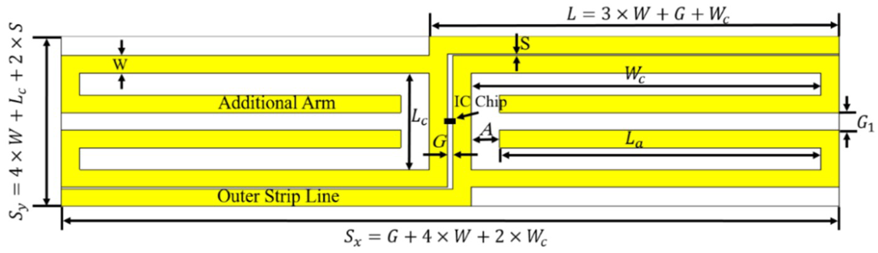
2. Antenna Structure

The miniature folded dipole tag antenna shown in Figure 1 is proposed for metallic objects designed for the European band. The PTFE substrate has been used to fabricate the tag antenna having dielectric constant of 2.55 ( tan δ = 0.0015 at test frequency 10 GHz). The thickness of substrate is 1.5 mm. Symmetric C-shaped resonators with additional arms and outer strip lines have formed the proposed compact tag antenna, with the additional arms positioned inside the C-shaped resonators and connected to the resonator from one side. The upper/lower outer strip lines are aligned with the horizontal arms of the folded dipole and are connected with the left/right arm of the folded dipole, respectively. The IC chip is attached between the folded dipole ( G = 0.5   mm ) in the middle side of the layout. The width W c and length L c of C-shaped resonators are parametrically optimized to attain the final dimensions of the miniaturized tag antenna. The addition of the outer strip lines ( L = G + 3 × W + W c ) and additional arms ( L a = W c A ) to the C-shaped resonators is the key attribute to miniaturizing the size of the proposed tag antenna and attaining the optimum impedance match. The C-shaped resonators can be easily tuned to attain a match with the IC chip, forming the input impedance network. The input impedance matching is also capable of being precisely adjusted to work over any UHF region band by tuning the dimensions of the C-shaped resonators. All dimensions are as shown in Figure 1.

3. Design Procedure and Analysis
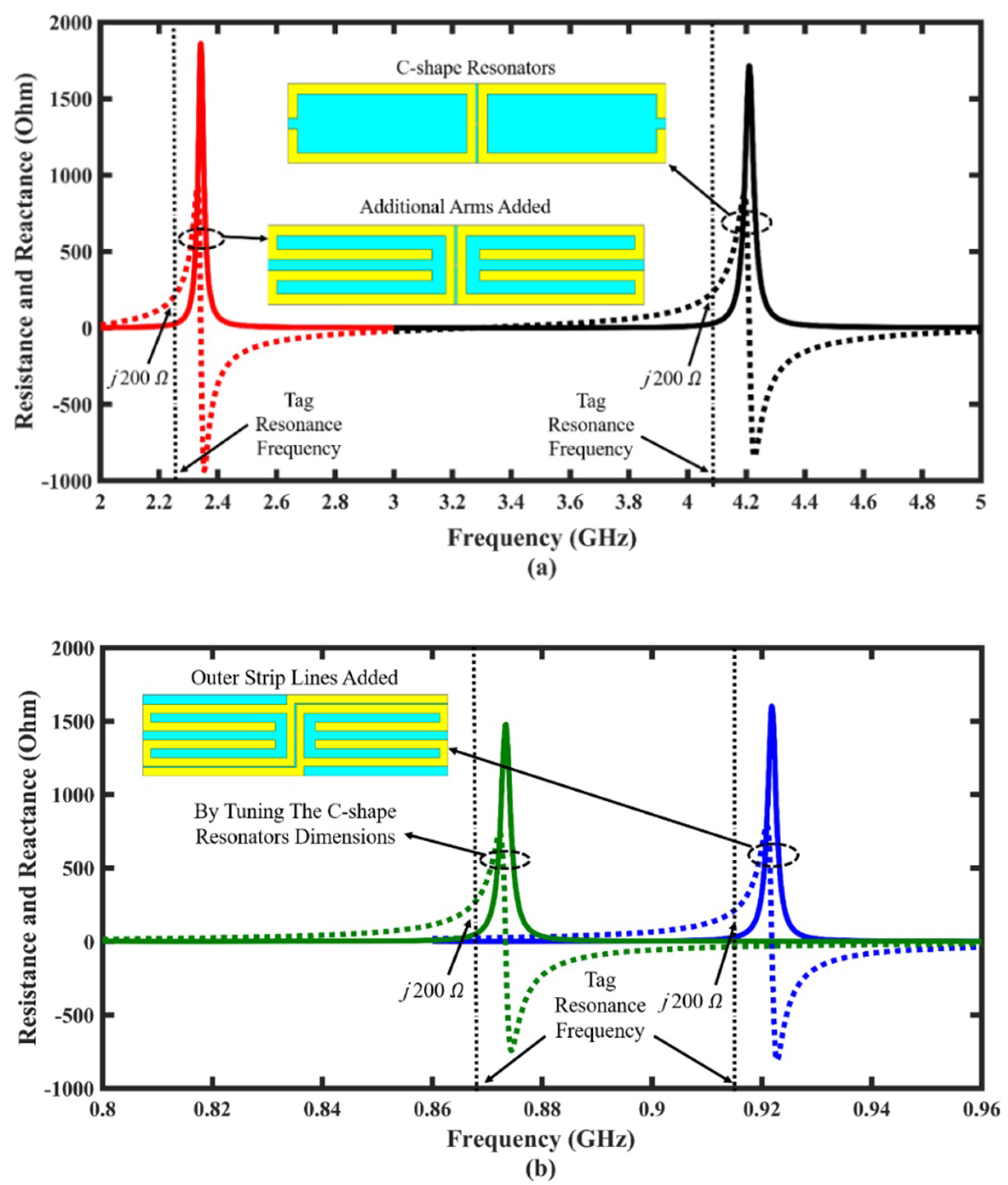
3.1. Design Stages

Computer Simulation Technology (CST) is employed to generate a simulation for the antenna design, which incorporates the Murata RFIDMAGICSTRAP LXMS31ACNA-011 tag chip (Murata Electronics, Kuala Lumpur, Malaysia) ( 25 j 200   at 886.5 MHz). The IC chip threshold power is 8   dB m . The tag antenna is placed on top of a 40 × 40   cm 2 perfect electrical conductor (PEC) that is 1 mm thick. The resonance frequency of an electrically small tag antenna is known to be commonly high, thus making it crucial for the operating frequency to be shifted down for utilization over UHF band frequencies. The designed procedure requires the current path to be increased by adding the additional arms and outer strip lines, whereby inductance of the tag antenna is increased by raising the surface current density [32], as illustrated in Figure 2. The first stage is initialized by simulating the folded dipole having two symmetric C-shaped resonators only, in which the IC chip is attached in the gap ( G = 0.5   mm ) between the resonators. The resonance frequency of this stage is found to be greater than 4.066 GHz as can be seen in Figure 2a. Thus, it could not be used for UHF RFID implementations. In the second stage, additional arms are added to the C-shaped resonators and consequently brought down the resonance frequency to 2.25   GHz . This is also shown in Figure 2a accordingly. The resonance frequency shifted down due to the effect of the increasing length (inductance) of the folded dipole antenna. The additional arms occupy the empty space inside the C-shaped resonators as shown in Figure 1, in which the space utilization is purposely done to miniaturize the size of the proposed antenna. Next, the third stage involves the tag antenna that is loaded with outer strip lines to bring down its resonance frequency over UHF band frequencies. This is shown in Figure 2b, which results in antenna impedance that matches the IC chip impedance. Such occurrence is due to the outer strip lines being utilized to minimize the S 11 response (less than 10   dB ). Therefore, the presence of the outer strip lines is considered as the main key attribute to realize an ideal reflection coefficient and impedance matching. The length of the additional arms ( L a = W a A ) and the outer stripe lines ( L = G + 3 × W + W c ) is related directly to the width of C-shaped resonators ( W c ), rendering them to be suitable for flexible tuning technique. Lastly, the dimensions of the C-shaped resonators ( L c and W c ) are forming the antenna impedance network, whereby the impedance matching can be realized between the antenna and IC chip by adjusting the dimensions precisely. Accuracy is ensured by ensuring that the length ( L c ) and width ( W c ) of C-shaped resonators that are parametrically optimized to achieve the impedance matching. The values of L c are correlated to a specific W c value to attain the desired S 11 response. Tuning the dimensions of the C-shaped resonators consequently brings down the tag antenna’s resonance frequency to 886.5   MHz . This is shown in Figure 2b, in which the resonance frequency is scaled down and fine-tuned by adjusting the dimensions of the C-shaped resonators to the desired centre frequency.

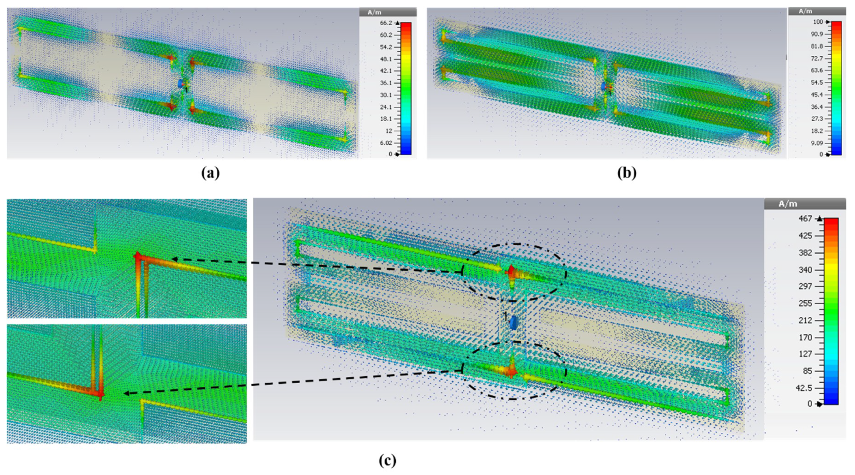
3.2. Current Analysis
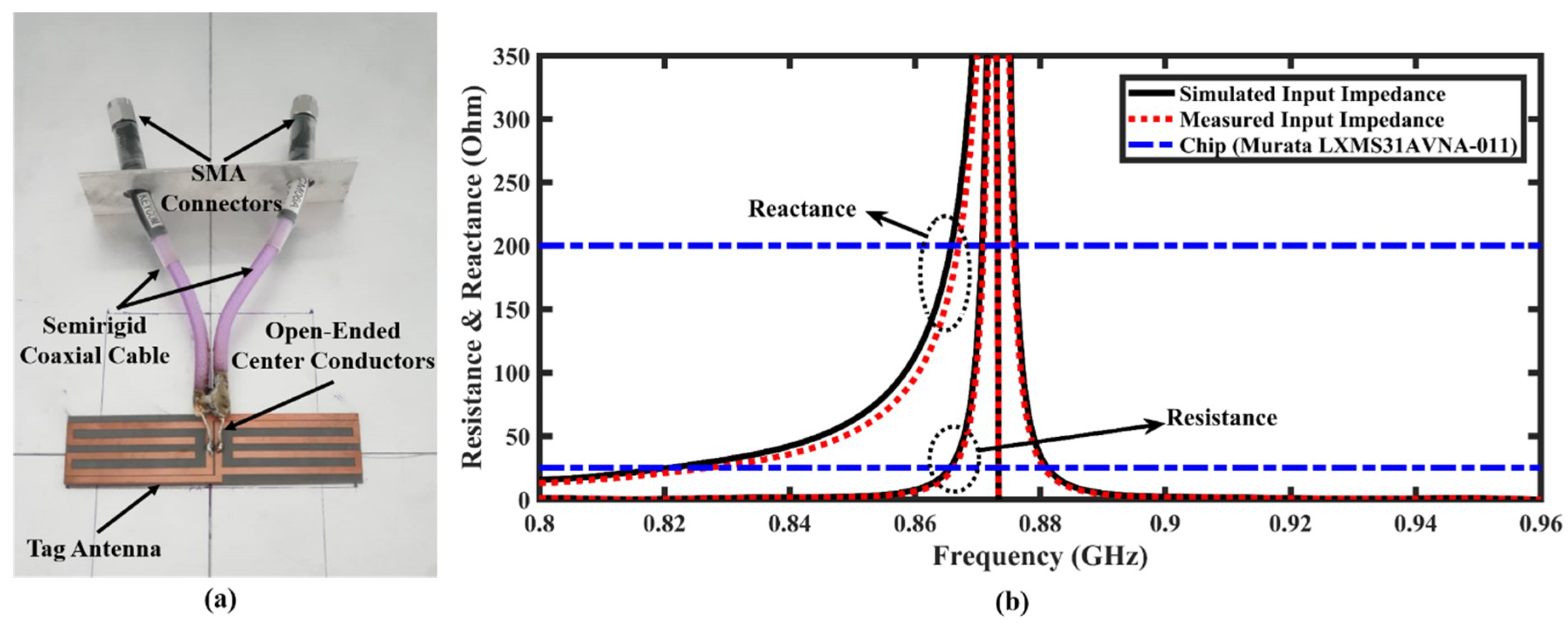
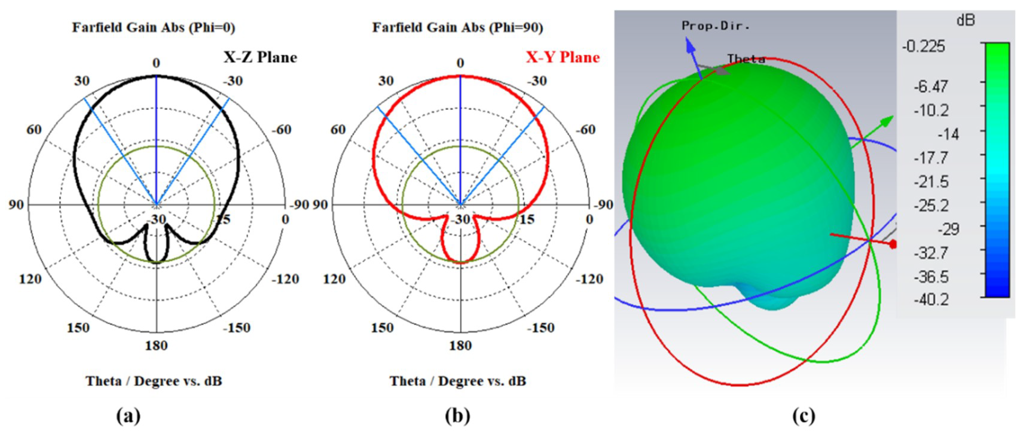
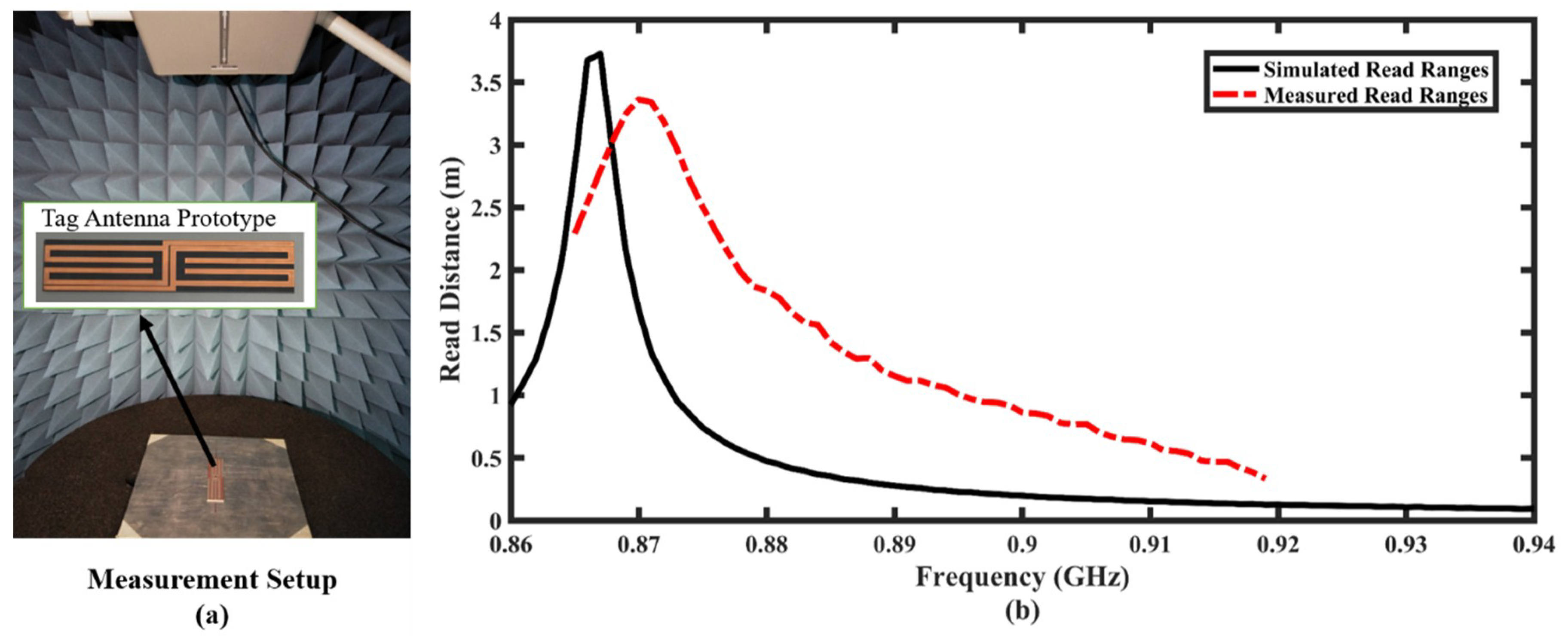
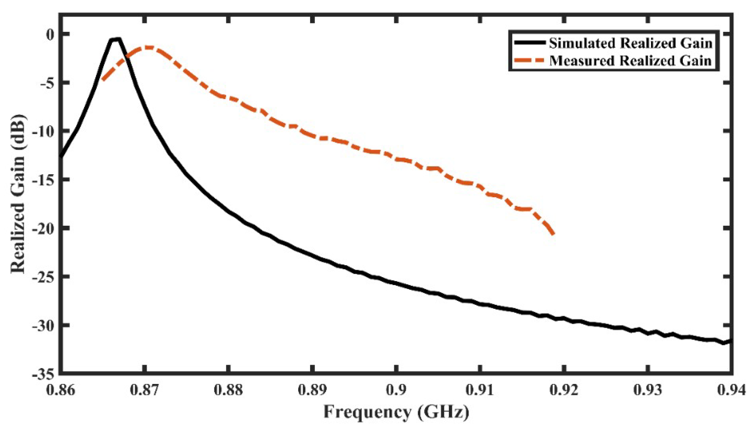
After presenting the design stages above, the corresponding surface current analysis of various design stages is explored here. As shown in Figure 3a, a lower surface current density of 66.2 A/m occurs when only the C-shape resonators are simulated (first stage). In the second stage, by adding the additional arms to the C-shaped resonators, the overall increase of inductance of the tag antenna takes place and is evident by increased current density in comparison to the first stage. Here, as shown in Figure 3b, the surface current value is 100 A/m, which is higher than the first design stage. It is to note that the surface currents plotted in Figure 3a,b have been plotted at corresponding resonance frequencies. Lastly, the simulated surface current on the miniaturized tag antenna when placed on a metallic plate is depicted in Figure 3c, at the resonance frequency of 866.5 MHz. The current path becomes longer after the addition of the additional arms and the outer strip lines, raising the tag antenna inductance further and resulting in a miniature size. Similarly, the resonance frequency is also shifted down over the UHF band, with the highest current density found on the outer strip lines and C-shaped resonators’ arms. This is an indication of their potential to be utilized for tuning the resonance frequency of the proposed tag antenna. Moreover, the presence of the outer strip lines is aimed at minimizing the reflection coefficient (less than 10   dB ) in order to realize the IC impedance. The dimensional adjustment of the C-shaped resonators effectively shifts down the resonance frequency to 866.5   MHz .

4. Test and Results

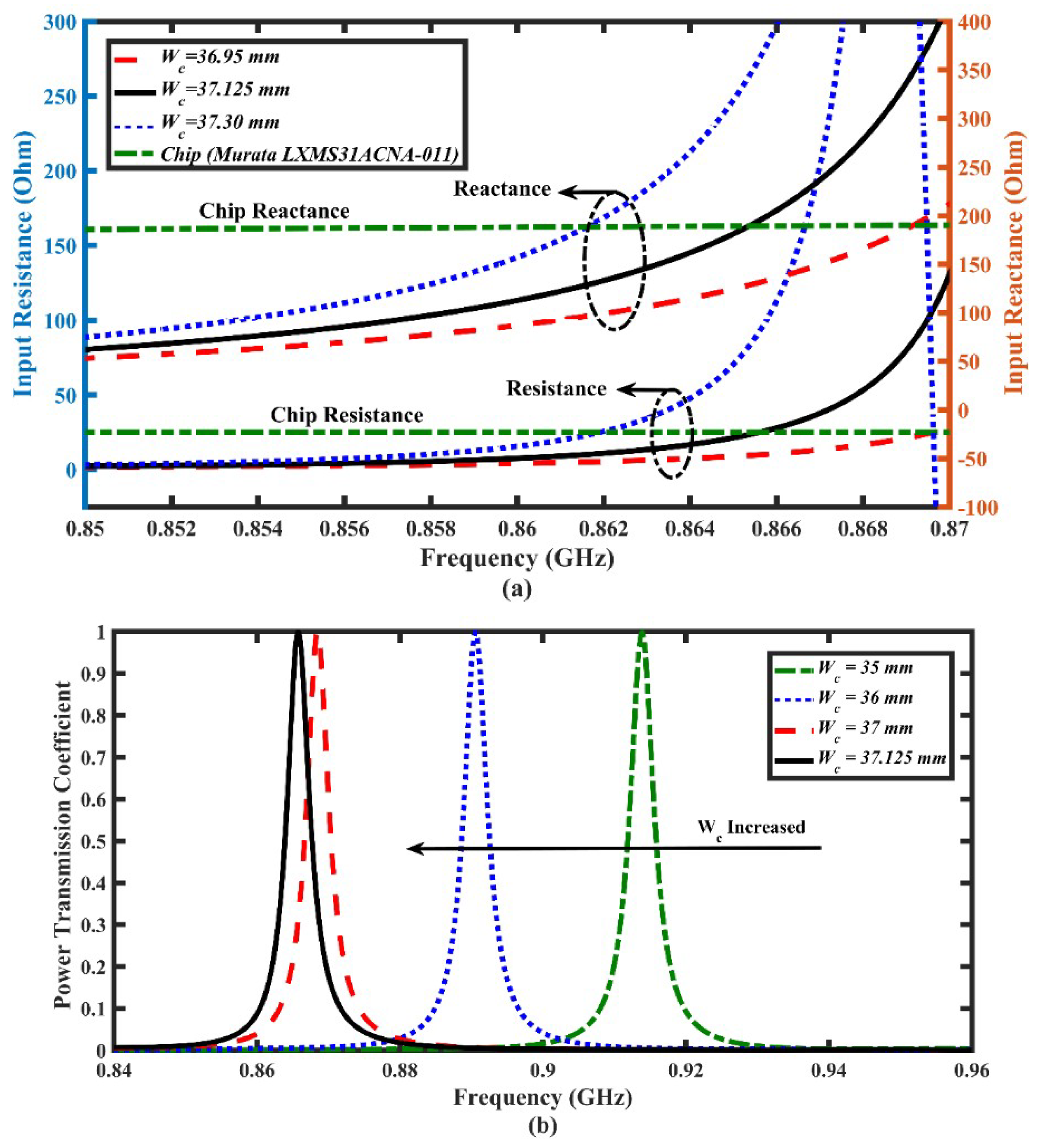
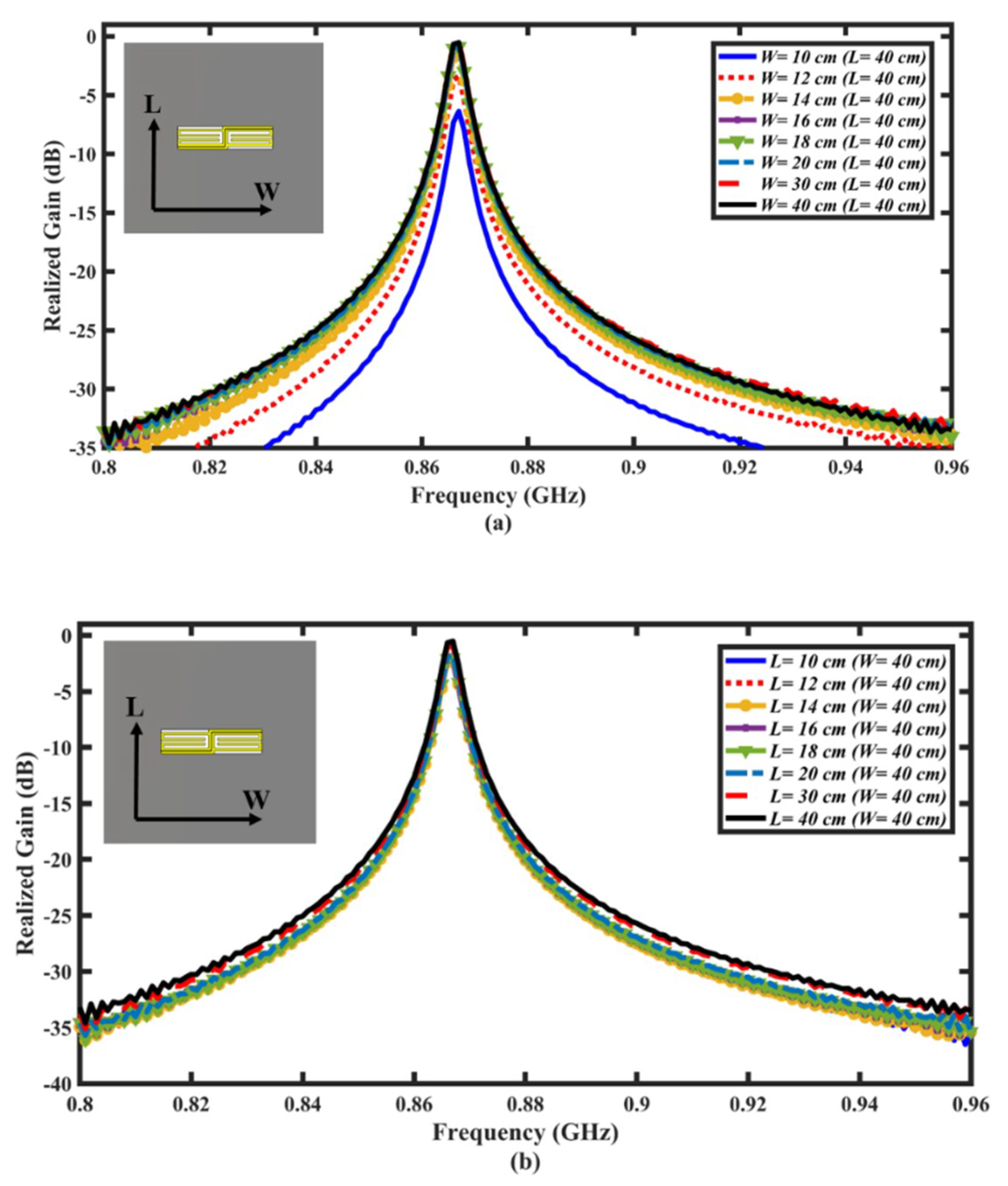
4.1. Parametric Study

The gain, input impedance, and antenna size have been studied in this work to design a UHF tag antenna. The design procedure includes four stages as presented in the previous section to design a miniaturized UHF RFID tag antenna design for the European band. The outer strip lines guarantee the reflection coefficient response of less than 10   dB , which ensures the possibility of attaining impedance matching. Meanwhile, the additional arms are used for miniaturization purposes, whereby the size of the proposed tag without them will be 86   mm × 61.7   mm . The number projected is in case of a tuned dimension of the C-shaped resonators at L c = 53.3   mm and W a = 38.75   mm , with the presence of outer strip lines. The presence of additional arms has reduced the antenna size by 69.6 % . The tag antenna’s input impedance is seen from the middle of the C-shaped resonators where the IC chip is placed; consequently, it requires a careful selection of the dimensions to attain a minimum S 11 response. The CST software has been used to perform the parametric analysis, using the L c and W c values as the crucial design parameters capable of affecting the input impedance and power transmission coefficient (τ). Varying W c in small increments results in antenna’s input impedance curves as depicted in Figure 4a. The variation in the reactance values is shown to exceed the differences in the resistance values; W c varied from 36.95   to   37.30   mm for the fixed L c value ( 11.1   mm ). The reactance and resistance of the tag antenna also increase when the value of W c increases. Meanwhile, the power transmission coefficient which is defined as the level of impedance matching for the tag antenna at the desired frequency remains unchanged at ( τ = 1 ). This can be seen in Figure 4b where W c is varied from 35   to   37.125   mm . From the above parametric analysis, it can be inferred that the tag antenna’s input impedance can be conjugately matched to the IC chip’s impedance by using careful selection of L c and W c values.

4.2. Simulated and Measured Results

The differential probe method [33] as shown in Figure 5a is utilized to measure the tag antenna’s input impedance due to it being a practical and cheap technique. As displayed in Figure 5a, the open-ended centre-conductors of the two ports are soldered to tag the antenna on one side and the other side is connected to the vector network analyser (VNA) through SMA ports. The tag antenna’s impedance is computed by measuring S-parameters of the equivalent two-port network and using the equation Z i n = ( 2 Z 0 ( 1 S 11 S 22 + S 12 S 21 S 12 S 21 ) ) / ( ( 1 S 11 ) ( 1 S 22 ) S 21 S 12 ) , where Z 0 is the coxial cable’s characteristic impedance. The tag antenna’s impedance is determined by measuring S-parameters, whereby the measured input impedance of the tag antenna is compared with that computed by the CST simulator. The results are shown in Figure 5b. The computed antenna impedance is 26 + j 198.9 while the measured antenna impedance is 21.1 + j 165.6 at resonance frequency of 866.5 MHz. A small discrepancy is observed between the simulated and measured tag antenna’s impedance, which may be caused by the soldering imperfection that exists between the antenna and the differential probe, or defects occurred during antenna fabrication.
The simulated radiation pattern of the miniaturized tag antenna at the resonance frequency is presented in Figure 6. The miniaturized folded dipole tag antenna is placed on a PEC sheet with a dimension of 40   cm × 40   cm , which resulted in the highest achieved gain of 0.225   dB at the boresight direction ( θ = 0 ° ). The X–Z and X–Y cutplanes for radiation patterns are depicted in Figure 6a,b respectively. The performance of the tag antenna is enhanced due to the metallic plate working as a reflector, reducing its back radiation.
The read distance is measured inside an anechoic chamber by utilizing the Voyantic Tagformance system. The miniaturized tag antenna is attached to the centre of the metal plate of 40   cm   ×   40   cm size inside the chamber, as shown in Figure 7a. The distance between the tag antenna and reader is 0.5 m, in which the detection distance expresses the tag antenna’s read range. This can be calculated by using the Friis formula, r = ( λ / 4 π ) P E I R P × G a × τ / P t h , where λ is the wavelength, P t h is the threshold power of the selected IC chip, P E I R P refers to the reader allowable output power for RFID (3.28 W), and G a is the tag antenna’s gain. The computed read distance is verified with the measured results over a frequency range of 865.6   MHz 867.6   MHz as presented in Figure 7b. The computed read range for the 40   cm × 40   cm metal sheet is 3.73   m , while the maximum measured detection distance of the tag antenna is up to 3.36   m . The frequency difference between simulated and measured results may be due to fabrication defects and variations of chip impedance, which are common in actual implementation. A discrepancy of 10 % is found between the simulated and measured results, where the IC chip’s operation frequency is from 865   MHz 955   MHz while the simulated results presented from 860   MHz   to   960   MHz . The results in Figure 7b have also proven that the measured read distance correlates satisfactorily with the simulated read distance plot.
The realized gain ( G r ) can be calculated by using G r = G a × τ , taking into account of the impedance mismatch between the chip and the antenna. It is considered one of the vital parameters for evaluating the miniaturized tag antenna’s performances. The results in Figure 8 show that the simulated and measured realized gain of the proposed tag antenna at the desired frequency are achieved at 0.53   dB and 1.41   dB , respectively. The discrepancy between the simulated and the measured results can be attributed to the mismatched losses. Changing the dimensions ( L × W ) of the backing metal is investigated here to see the effects on the performance of the proposed tag antenna. Firstly, the width (W) of the backing metallic surface is varied from 10   cm   to   40   cm while the length (L) is fixed at 40   cm . The effect is exhibited in Figure 9a. The maximum realized gain is 0.53   dB at the resonance frequency. Varying the length of the metallic surface exhibits similar effects on the performance of the tag antenna when L is changed from 10   cm to 40   cm ( W = 40   cm is fixed). This is shown in Figure 9b. These results show that the presented tag antenna’s operating frequency is not affected with the variation of the dimensions of the metallic surface, which is preferable for metal-mountable applications of the tag antenna.

5. Discussion

Table 1 exhibits a comparison of the miniature folded dipole with tag antennas attached to metallic objects in terms of the antenna structure, volume, realized gain, and read range. In [21], a small electrical tag antenna on a dual-layer substrate is constructed using two PIFA array radiators and a loaded via-patch, respectively, for impedance matching purposes. Meanwhile, the dual-layer tag antenna in ref. [34] consists of two slotted PIFAs and a middle layer embedded, with a slotted patch for miniaturizing purposes. Similarly, a compact dual-layer antenna comprised of four PIFAs and stub lines shorted to the ground for impedance matching goal is presented in [23], whereas, in [7], a folded dipole antenna with a centre gap placed on the AMC substrate is proposed. All of these studies [7,21,23,34] have been constructed to be dual-layer in nature, have metallic vias, and have a profile-thickness > 2   mm . Such thickness is generally not preferred to be mountable into a metallic surface. Furthermore, the use of metallic vias renders the tuning of the antenna’s input impedance and its resonance frequency to be tedious. Similarly, its cost has increased significantly despite the smaller antenna size. The works presented in refs. [30,35,36] comprised of a single substrate with a number of vias of thickness less than 2 mm. The best realized gain is recorded at 1.63   dB in [36], but its configuration utilizes eight metallic vias that consequently raised the level of complexity and its cost. Meanwhile, the works presented in refs. [24,25,26,28,32,37] have used folding polyethylene terephthalate (PET) around the foam without requiring any metallic vias or shorting pins. However, the best achieved realized gain is 1   dB for the designed work in ref. [25] at a thickness of 3   mm , which is not preferred for a metal mountable tag antenna. Therefore, the simple configuration shown in the proposed miniaturized folded dipole in our work does not require metallic vias or shorting walls. It is fabricated on a PTFE substrate of 1.5   mm thickness, ensuring the suitability of its configuration to be mountable on metallic objects. Moreover, its operation is realized with a flexible tuning technique, recording a higher realized gain compared to previous literature. The detection distance can also be further improved by incorporating a microchip that offers better reading sensitivity. Nevertheless, in comparison to the other literature, the proposed miniaturized folded dipole has been successfully implemented on metallic objects and offers the advantages of having only one layer with simple structure and comparable gain and size. In addition, since the design does not incorporate any complex fabrication technique unlike previously reported designs, based on its low complexity, the design is suitable for mass production.

6. Conclusions

This paper has proposed a miniature folded dipole tag antenna that is capable of functioning while being mounted to metal objects over UHF European band. The miniaturized size is achieved without relying on shorting the radiator to the ground layer using vias or pins. Furthermore, its configuration is inexpensive, easy to fabricate, and is characterized by a low profile with a thickness of 1.5 mm. The outer strip lines have guaranteed a good impedance matching with IC chip while tuning the dimensions of the C-shaped resonators have introduced a flexible control for the resonance frequency. Lastly, the realized gain that is achieved by the tag antenna when attached to a 40   cm × 40   cm sheet is 0.53   dB . Therefore, the proposed miniature folded dipole tag antenna can be considered as an acceptable candidate for RFID applications mounted onto metal sheets.

Author Contributions

Conceptualization, F.E., E.H. and R.S.; methodology, F.E., E.H. and R.S.; investigation, F.E. and H.U.; resources, F.E. and E.-H.L.; data curation, F.E.; writing—original draft preparation, F.E.; writing—review and editing E.H., H.U., and W.A.W.M.M.; supervision, E.H., W.A.W.M.M., S.W.H. and E.-H.L.; funding acquisition, E.H., W.A.W.M.M., S.W.H., and M.Z.H.M.

Acknowledgments

This work is supported by the University of Malaya Research University Grant-Faculty Programme under Grant No. RF005A-2018, University of Malaya Faculty Research Grant under Grant No. GPF029A-2018, and University Malaysia Sabah (UMS).

Conflicts of Interest

The authors declare no conflict of interest.

References

  1. Hamani, A.; Yagoub, M.C.E.; Vuong, T.P.; Touhami, R. A novel broadband antenna design for UHF RFID tags on metallic surface environments. IEEE Antennas Wirel. Propag. Lett. 2017, 16, 91–94. [Google Scholar] [CrossRef]
  2. Gao, X.; Shen, Z. UHF/UWB tag antenna of circular polarization. IEEE Trans. Antennas Propag. 2016, 64, 3794–3802. [Google Scholar] [CrossRef]
  3. Hu, W.; Wen, G.; Inserra, D.; Huang, Y.; Li, J.; Chen, Z. A circularly polarized antenna array with gain. Electronics 2019, 8, 400. [Google Scholar] [CrossRef]
  4. Salman, K.N.; Ismail, A.; Abdullah, R.S.A.R.; Saeedi, T. Coplanar UHF RFID tag antenna with U-shaped inductively coupled feed for metallic applications. PLoS ONE 2017, 12, e0178388. [Google Scholar] [CrossRef] [PubMed]
  5. Liu, M.; Ma, L.; Wang, N.; Zhang, Y.; Yang, Y.; Wang, H. Passive multiple target indoor localization based on joint interference cancellation in an RFID system. Electronics 2019, 8, 426. [Google Scholar] [CrossRef]
  6. Yu, B.; Kim, S.-J.; Jung, B.; Harackiewicz, F.J.; Lee, B. RFID tag antenna using two-shorted microstrip patches mountable on metallic objects. Microw. Opt. Technol. Lett. 2007, 49, 414–416. [Google Scholar] [CrossRef]
  7. Kim, D.; Yeo, J. Low-profile RFID tag antenna using compact AMC substrate for metallic objects. IEEE Antennas Wirel. Propag. Lett. 2008, 7, 718–720. [Google Scholar]
  8. Ukkonen, L.; Sydänheimo, L.; Kivikoski, M. Effects of metallic plate size on the performance of microstrip patch-type tag antennas for passive RFID. IEEE Antennas Wirel. Propag. Lett. 2005, 4, 410–413. [Google Scholar] [CrossRef]
  9. Kamalvand, P.; Pandey, G.K.; Meshram, M.K.; Mallahzadeh, A. A single sided dual-antenna structure for UHF RFID tag applications. Int. J. RF Microwave Comput.-Aided Eng. 2015, 25, 619–628. [Google Scholar] [CrossRef]
  10. Benmessaoud, L.; Vuong, T.P.; Yagoub, M.C.E.; Touhami, R. A novel 3-D tag with improved read range for UHF RFID localization applications. IEEE Antennas Wirel. Propag. Lett. 2017, 16, 161–164. [Google Scholar] [CrossRef]
  11. Bilgiç, M.M.; Yeğin, K. An HF/UHF dual mode RFID transponder antenna and HF range extension using UHF wireless power transmission. Turkish J. Electr. Eng. Comput. Sci. 2016, 24, 3949–3960. [Google Scholar] [CrossRef]
  12. Ennasar, M.A.; Aznabet, I.; el Mrabet, O.; Essaaidi, M. Design and characterization of a compact single layer modified S-shaped tag antenna for UHF-RFID applications. Adv. Electromagn. 2019, 8, 59–65. [Google Scholar] [CrossRef]
  13. Lin, Y.F.; Chang, M.J.; Chen, H.M.; Lai, B.Y. Gain Enhancement of Ground Radiation Antenna for RFID Tag Mounted on Metallic Plane. IEEE Trans. Antennas Propag. 2016, 64, 1193–1200. [Google Scholar] [CrossRef]
  14. Koo, T.W.; Kim, D.; Ryu, J.I.; Seo, H.M.; Yook, J.G.; Kim, J.C. Design of a label-typed UHF RFID tag antenna for metallic object. IEEE Antennas Wirel. Propag. Lett. 2011, 10, 1010–1014. [Google Scholar]
  15. Niew, Y.-H.; Lee, K.-Y.; Lim, E.-H.; Bong, F.-L.; Chung, B.-K. Patch-loaded semicircular dipolar antenna for metal-mountable UHF RFID tag design. IEEE Trans. Antennas Propag. 2019, 1. [Google Scholar] [CrossRef]
  16. Rao, K.V.S.; Lam, S.F.; Nikitin, P.V. Wideband metal mount UHF RFID tag. In IEEE Antennas and Propagation Society International Symposium; IEEE: Piscataway, NJ, USA, 2008; pp. 1–4. [Google Scholar]
  17. Jankowski-Mihułowicz, P.; Kawalec, D.; Wȩglarski, M. Antenna design for semi-passive UHF RFID transponder with energy harvester. Radioengineering 2015, 24, 722–728. [Google Scholar] [CrossRef]
  18. Gao, B.; Yuen, M.M.F. Passive UHF RFID packaging with electromagnetic band gap (EBG) material for metallic objects tracking. IEEE Trans. Compon. Packag. Manuf. Technol. 2011, 1, 1140–1146. [Google Scholar] [CrossRef]
  19. Kuo, S.K.; Liao, L.G. An analytic model for impedance calculation of an RFID metal tag. IEEE Antennas Wirel. Propag. Lett. 2010, 9, 603–607. [Google Scholar] [CrossRef]
  20. Kwon, H.; Lee, B. Compact slotted planar inverted-F RFID tag mountable on metallic objects. Electron. Lett. 2005, 41, 1308–1310. [Google Scholar] [CrossRef]
  21. Zhang, J.; Long, Y. A novel metal-mountable electrically small antenna for RFID tag applications with practical guidelines for the antenna design. IEEE Trans. Antennas Propag. 2014, 62, 5820–5829. [Google Scholar] [CrossRef]
  22. Kim, J.S.; Choi, W.; Choi, G.Y. UHF RFID tag antenna using two PIFAs embedded in metallic objects. Electron. Lett. 2008, 44, 1181–1182. [Google Scholar] [CrossRef]
  23. Zhang, J.; Long, Y. A dual-layer broadband compact UHF RFID tag antenna for platform tolerant application. IEEE Trans. Antennas Propag. 2013, 61, 4447–4455. [Google Scholar] [CrossRef]
  24. Moh, C.-W.; Lim, E.-H.; Bong, F.-L.; Chung, B.-K. Miniature coplanar-fed folded patch for metal mountable UHF RFID tag. IEEE Trans. Antennas Propag. 2018, 66, 2245–2253. [Google Scholar] [CrossRef]
  25. Ng, W.H.; Lim, E.H.; Bong, F.L.; Chung, B.K. E-shaped folded-patch Antenna with multiple tuning parameters for on-metal UHF RFID tag. IEEE Trans. Antennas Propag. 2018, 67, 56–64. [Google Scholar] [CrossRef]
  26. Bong, F.L.; Lim, E.H.; Lo, F.L. Compact folded dipole with embedded matching loop for universal tag applications. IEEE Trans. Antennas Propag. 2017, 65, 2173–2181. [Google Scholar] [CrossRef]
  27. Erman, F.; Ismail, A.; Abdullah, R.S.A.R.; Alhawari, A.R.H.; Shabaneh, A.; Mohamed, N. UHR RFID spilt-ring resonator-based tag antenna with photonic bandgap structure for metallic objects. J. Fundam. Appl. Sci. 2017, 9, 630–636. [Google Scholar] [CrossRef]
  28. Bong, F.L.; Lim, E.H.; Lo, F.L. Flexible folded-patch Antenna with serrated edges for metal-mountable UHF RFID tag. IEEE Trans. Antennas Propag. 2017, 65, 873–877. [Google Scholar] [CrossRef]
  29. Son, H.-W.; Pyo, C.-S. Design of RFID tag antennas using an inductively coupled feed. Electron. Lett. 2005, 41, 994–996. [Google Scholar] [CrossRef]
  30. Genovesi, S.; Monorchio, A. Low-profile three-arm folded dipole antenna for UHF band RFID tags mountable on metallic objects. IEEE Antennas Wirel. Propag. Lett. 2010, 9, 1225–1228. [Google Scholar] [CrossRef]
  31. Lee, S.R.; Lim, E.H.; Bong, F.L.; Chung, B.K. Slotted circular patch with multiple loading stubs for platform insensitive tag. IEEE Trans. Antennas Propag. 2018, 66, 5072–5079. [Google Scholar] [CrossRef]
  32. Ng, W.H.; Lim, E.H.; Bong, F.L.; Chung, B.K. Folded patch Antenna with tunable inductive slots and stubs for UHF tag design. IEEE Trans. Antennas Propag. 2018, 66, 2799–2806. [Google Scholar] [CrossRef]
  33. Alhawari, A.R.H.; Ismail, A.; Jalal, A.S.A.; Abudullah, R.S.A.R.; Rasid, M.F.A. U-shaped inductively coupled feed radio frequency identification tag antennas for gain enhancement. Electromagnetics 2014, 34, 487–496. [Google Scholar] [CrossRef]
  34. Zhang, J.; Long, Y. A miniaturized via-patch loaded dual-layer rfid tag antenna for metallic object applications. IEEE Antennas Wirel. Propag. Lett. 2013, 12, 1184–1187. [Google Scholar] [CrossRef]
  35. Yang, E.-S.; Son, H.-W. Dual-polarised metal-mountable UHF RFID tag antenna for polarisation diversity. Electron. Lett. 2016, 52, 496–498. [Google Scholar] [CrossRef]
  36. Zeng, W.; Zhao, J.; Ke, B.; Wu, Q. Compact microstrip RFID tag antenna mountable on metallic objects. Procedia Eng. 2011, 16, 320–324. [Google Scholar] [CrossRef]
  37. Lee, S.R.; Lim, E.H.; Bong, F.L.; Chung, B.K. Slotted folded patch antenna with double-t-slots for platform insensitive UHF tag design. IEEE Trans. Antennas Propag. 2018, 67, 670–675. [Google Scholar] [CrossRef]
Figure 1. Geometry of the miniature folded dipole tag antenna S x = 82.75 , S y = 19.5 , W c = 37.125 , L c = 11.1 , W = 2 , A = 3 , S = 0.2 , G = 0.5 , G 1 = 2 (unit: mm).
Electronics 08 00713 g001
Figure 2. (a) input impedance for the stages with C-shaped resonators and additional arms; (b) input impedance for the stages with outer strip lines and tuning the dimensions of C-shaped resonators (Solid line: Resistance, Dotted line: Reactance).
Electronics 08 00713 g002
Figure 3. Tag antenna’s surface current distribution at the resonance frequency for design procedure; (a) first stage, (b) second stage and (c) final stage.
Electronics 08 00713 g003
Figure 4. (a) simulated antenna’s input impedance for different W c values; (b) power transmission coefficient for various W c values.
Electronics 08 00713 g004
Figure 5. (a) differential probe method; (b) simulated and measured tag antenna’s impedance.
Electronics 08 00713 g005
Figure 6. Simulated radiation pattern at resonance frequency for the miniature tag antenna; (a) X–Z plane; (b) X–Y plane; and (c) radiation pattern.
Electronics 08 00713 g006
Figure 7. (a) the measurement setup; (b) the computed and measured detection distances.
Electronics 08 00713 g007
Figure 8. The simulated and measured realized gains of the tag antenna.
Electronics 08 00713 g008
Figure 9. The simulated realized gain (a) varying the length of backing metal for fixed width; (b) varying the width of the backing metal for fixed length.
Electronics 08 00713 g009
Table 1. Comparing the performance of the metallic mountable tag antennas.
Reference Tag   Dimension   ( mm ) Tag   Volume   ( mm 3 ) Substrate P E I R P   ( W ) P i c ( d B m ) Realized Gain (dB)Read Rang (m)
[21] 26 × 14 × 2.4 873.6FR4 + PTFE4−1505.2
[34] 28 × 14 × 3.2 1254.4FR44−15−11.21.8
[23] 56 × 26 × 3.2 4659.2FR44−15−3.84
[7] 67 × 34.4 × 3.52 8112.9Taconic RF-60 + Foam--−0.74.8
[30] 69.5 × 14 × 1.5 1459.5FR42−15−9.662.2
[35] 64 × 64 × 2 8192FR44−17.4−1.1810.2
[36] 60 × 45 × 1.6 4320FR44-1.636.2
[24] 40 × 25 × 3 3000PET + Foam4−17.8−0.910.7
[25] 30 × 30 × 3 2700PET + Foam4−20114.5
[26] D = 31   mm 4828PET + Foam3.28−20−181.8
[28] 30 × 30 × 3 2700PET + Foam4−17.8−57.2
[32] 40 × 40 × 1.6 2560PET + Foam3.28−20−86.3
[37] 42 × 50 × 1.6 3360PET + Foam4−20−105.2
Proposed 82.75 × 19.5 × 1.5 2420PTFE3.28−8−0.533.72

