Article

The Room Temperature Multi-Channel Heterodyne Receiver Section of the PHAROS2 Phased Array Feed

1
National Institute for Astrophysics (INAF), Astronomical Observatory of Cagliari, Via della Scienza 5, 09047 Selargius, Italy
2
National Institute for Astrophysics (INAF), Institute of Radio Astronomy, Via P. Gobetti 101, 40129 Bologna, Italy
3
Italian Space Agency (ASI), Via del Politecnico snc, 00133 Roma, Italy
*
Author to whom correspondence should be addressed.
Electronics 2019, 8(6), 666; https://doi.org/10.3390/electronics8060666
Submission received: 9 May 2019 / Revised: 24 May 2019 / Accepted: 6 June 2019 / Published: 12 June 2019
(This article belongs to the Section Microwave and Wireless Communications)

Abstract

:
This paper describes the design, fabrication, and test results of a room temperature multi-channel heterodyne receiver operating across the 2.3–8.2 GHz radio frequency (RF) band. Such a “Warm Section” (WS) receiver is part of phased arrays for reflector observing systems 2 (PHAROS2), a C-band phased array feed (PAF) demonstrator with digital beamformer for radio astronomy application. The WS receiver is cascaded to the PHAROS2 cryostat, which includes an array of Vivaldi antennas with low noise pre-amplification stages. The WS can handle up to 32 RF signals and, for each of them, realizes the operations of filtering, RF amplification and down-conversion from the RF to the 375–650 MHz intermediate frequency (IF). Also, the WS incorporates an IF-to-optical signal conversion through analogue wavelength division multiplexing IF over fiber (IFoF) and fiber-optic transmitters (OTXs). The 32-channel WS receiver consists of four eight-channel WS RF/IF modules, one local oscillator (LO) splitter module and one monitoring and control module, all hosted in a standard 6U × 19-inch rack.

1. Introduction

High-sensitivity large-scale surveys are an essential tool for new discoveries in radio astronomy.
A phased array feed (PAF) placed at the focal plane of an antenna can increase the field-of-view (FoV) and the mapping efficiency by fully sampling the sky [1,2,3]. A typical PAF consists of few hundred closely packed antenna elements with about half wavelength element separation that, by spatially sampling the focal plane, can synthesize multiple independent beams and be set to Nyquist-sample the sky. Through a beam-forming process, PAFs are capable of electronic steering and optimization of the antenna illumination to provide high-quality far-field patterns for each of the beams. An example of two new generation radio astronomy facilities operating L-band PAFs at room temperature with digital beamformers are described in references [4,5].
PHAROS (phased arrays for reflector observing systems) [6,7,8,9] is a cryogenically cooled PAF demonstrator with analogue beamformer based on an array of dual polarization 10 × 11 Vivaldi antennas (see a picture in Figure 1) designed for radio astronomy observations across the 4–8 GHz band. The Vivaldi array utilizes high-performance Taconic printed circuit boards (PCBs) based on a three-layer laminated board structure. The complete PHAROS focal plane array was built with 11 boards in both the x and the y directions, each integrating 10 Vivaldi antenna elements with 21 mm spacing. The spacing-to-wavelength ratio is 0.56 at the PHAROS maximum operating frequency of 8 GHz (λmin = 37.5 mm). The overall size of the array on the x-y plane is ≈ 230 × 230 mm2, i.e., 6λmin × 6λmin (and equivalently 3λmax × 3λmax for λmax = 75 mm, relative to the 4 GHz minimum frequency). Only a sub-set of 24 elements of the array with same polarization is populated with cryogenic low noise amplifiers (LNAs), while the non-active elements are terminated into 50 Ω loads. The non-active elements add negligible noise contribution due to their low operating temperature of ≈20 K.
The PHAROS upgraded version, PHAROS2 [10], utilizes new components to reduce the system noise temperature, enhance the aperture efficiency and digitize the signals from a sub-array of 24 single-polarization PAF antenna elements that synthesize four independent single polarization beams. PHAROS2 is being developed in the framework of the PAF SKA (Square Kilometer Array) [11] advanced instrumentation program as a technology demonstrator resulting from the international collaboration between the Italian National Institute for Astrophysics (INAF), Jodrell Bank Observatory at the University of Manchester (UK), ASTRON (the Netherlands), the University of Malta (Malta) and the University of Chalmers (Sweden).
A block diagram of the PHAROS2 system is illustrated in Figure 2. The Warm Section (WS) is the signal chain section located between the cryogenically cooled PHAROS2 antenna array and the digital beamformer that will enable first-ever radio astronomy observation in C-band with a phased array feed. PHAROS2 features the following:
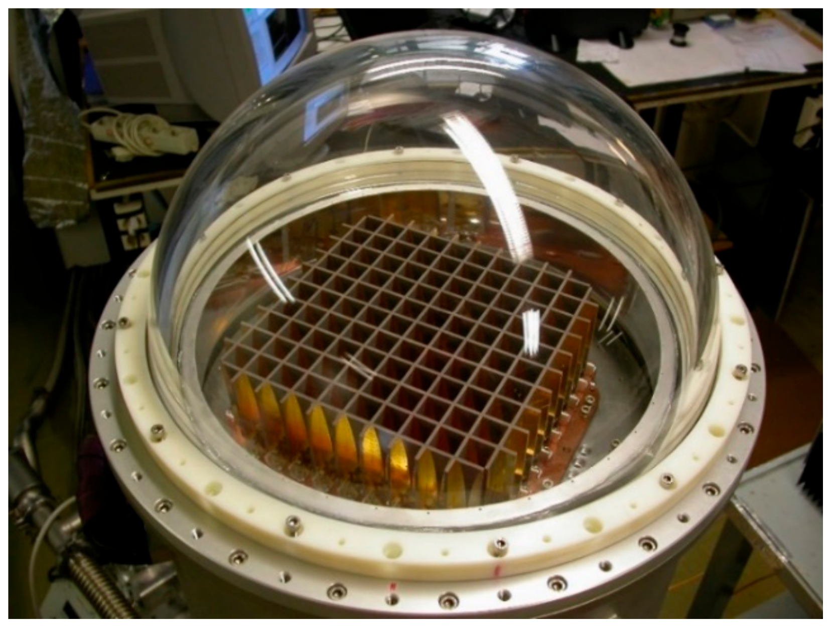
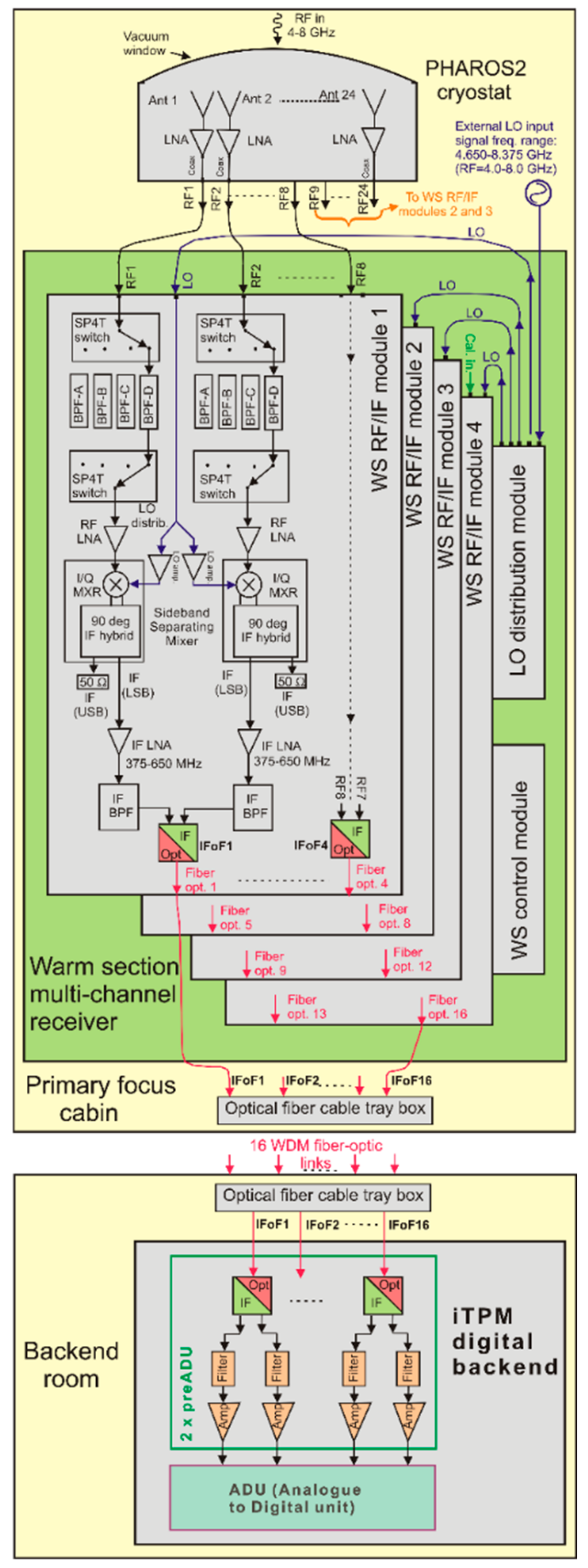
  • A 4–8 GHz cryogenic section comprising an array of Vivaldi antennas cascaded with new LNAs with state-of-the-art performance (noise temperature Tn = 2.3 K typical);
  • A 2.3–8.2 GHz room-temperature WS multi-channel receiver, described in this paper;
  • An Italian tile processing module (iTPM) digital backend based on a field programmable gate array (FPGA) that is capable of digitizing and forming four independent beams across a ≈275 MHz IF band [12].
We note that the frequency range of the WS receiver, 2.3–8.2 GHz (fmax/fmin ≈ 3.6), is larger than the one delivered by the PHAROS2 Vivaldi array cryogenic section (4–8 GHz). Therefore, the WS and associated digital backend can be used not only with PHAROS2, but also with other PAF antenna arrays that could be developed to cover 2.3–8.2 GHz or part of such frequency range. A single “high-frequency” PAF array operating at frequencies greater than ≈3 GHz with few hundred antenna elements would require few WS receivers connected in parallel to pre-filter and downconvert multiples of 32 × RF input signals to a frequency range suitable for digitization and further processing by a backend. Currently, the WS is a necessary piece of hardware for PAFs designed to operate beyond few GHz, as a direct sampling of the RF signal by analog to digital converters (ADCs) is only possible up to several GHz [13]. The existing high-performance ADCs have enough bits of resolution (typically 8–12) to operate in moderate RFI environment, but limited bandwidth and maximum frequency, which makes them suitable solutions for PAFs radio astronomy application up to S-band (or lower frequency), but not yet for 4–8 GHz or beyond. This is likely to change in the near future as the current technology trends of development of ADCs with continuously higher sampling frequency and sufficient bit resolution might soon allow performing direct multichannel RF digitization (through direct sampling or interleaved sampling) of signals from PAF antennas operating at ≈10 GHz and beyond with frequency bandwidths of few GHz. Furthermore, a new generation of FPGA that incorporates ADC on chip, known as RFSoC (radio frequency system-on-chip) [14], is set to revolutionize the FPGA market sector and has great potential for use with PAFs.
The high amplification of the PHAROS2 cryogenic LNAs (Gain ≈ 39 dB) relaxes the noise temperature requirements of the WS receiver chain, which is designed to add a negligible contribution to the overall receiver noise.
In this paper, we describe the design and experimental results of the 2.3–8.2 GHz WS 32-channel receiver that we developed for PHAROS2.
In Section 2, we illustrate the WS multi-channel receiver specifications and its design and architecture. The WS fabrication, integration and assembly of the receiver sub-systems are presented in Section 3. The WS receiver characterization results and the conclusions are discussed in Section 4 and Section 5, respectively.

2. Design of Warm Section Multi-Channel Receiver

The main specifications of the Warm Section receiver, such as the number of RF channels, the RF band, the frequency conversion scheme, the local oscillator (LO) and intermediate frequency (IF) bands, the features of the filter bank and the characteristics of the control module, are listed in Table 1. The instrument is required to handle up to 32 RF input signals, although only 24 (plus 1 for calibration) will be used for PHAROS2.
A 3D view of the WS 32-channel receiver, equipped with all its modules, is given in Figure 3. The WS includes four eight-channel WS RF/IF modules, one LO distribution module and one WS monitor and control module arranged in a standard rack with a size of 6U × 19-inch (where 6 rack units = 266.7 mm). The receiver performs signal filtering by using a switched filter bank, signal conditioning, and single frequency down-conversion of a section of the 2.3–8.2 GHz RF band down to the 375–650 MHz IF band (275 MHz instantaneous bandwidth). The down-conversion scheme utilizes sideband separating mixers in lower side band (LSB), with the upper side band (USB) being internally terminated. The IF signals are converted to optical signals by an analogue wavelength division multiplexing (WDM) IFoF fiber-optic transmitter (OTX) that transports two IFs over a single optical fiber.
The switched filter bank on the WS receiver input section is used to mitigate the effects of the radio frequency interference (RFI) signals across the RF band that could otherwise saturate the receiver chain and the optical links. One of the four BPF filters, BPF-A, is specified to cover the broad 2.3–8.2 GHz RF frequency band, while the other three filters (BPF-B, -C and -D) have ≈275 MHz “narrowband” features (Table 1), with bands centered around astronomical lines. As we will see in the following sections, the selection of one of the narrowband filters allows to achieve an image sideband rejection greater than 50 dB, as a result of the combined effects of the filter rejection (≥30 dB for USB to LSB frequency separation of 2 × fIFmin = 750 MHz) and of the sideband separating mixer rejection (≥20 dB).

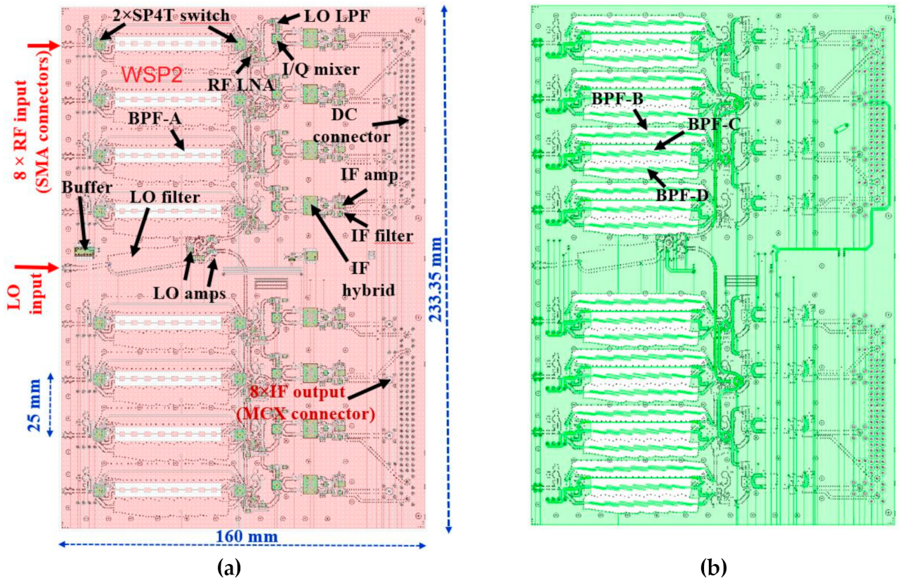
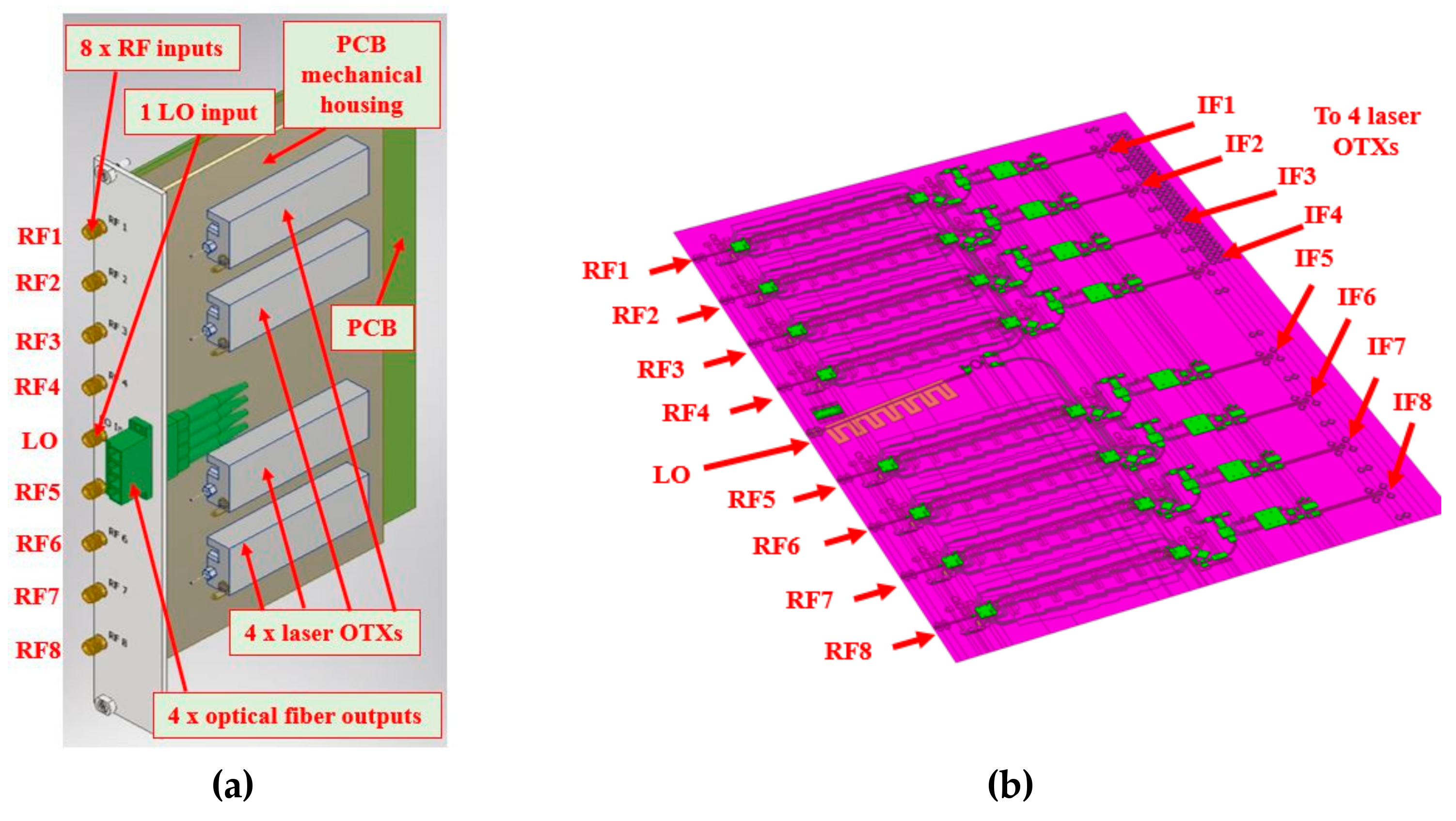
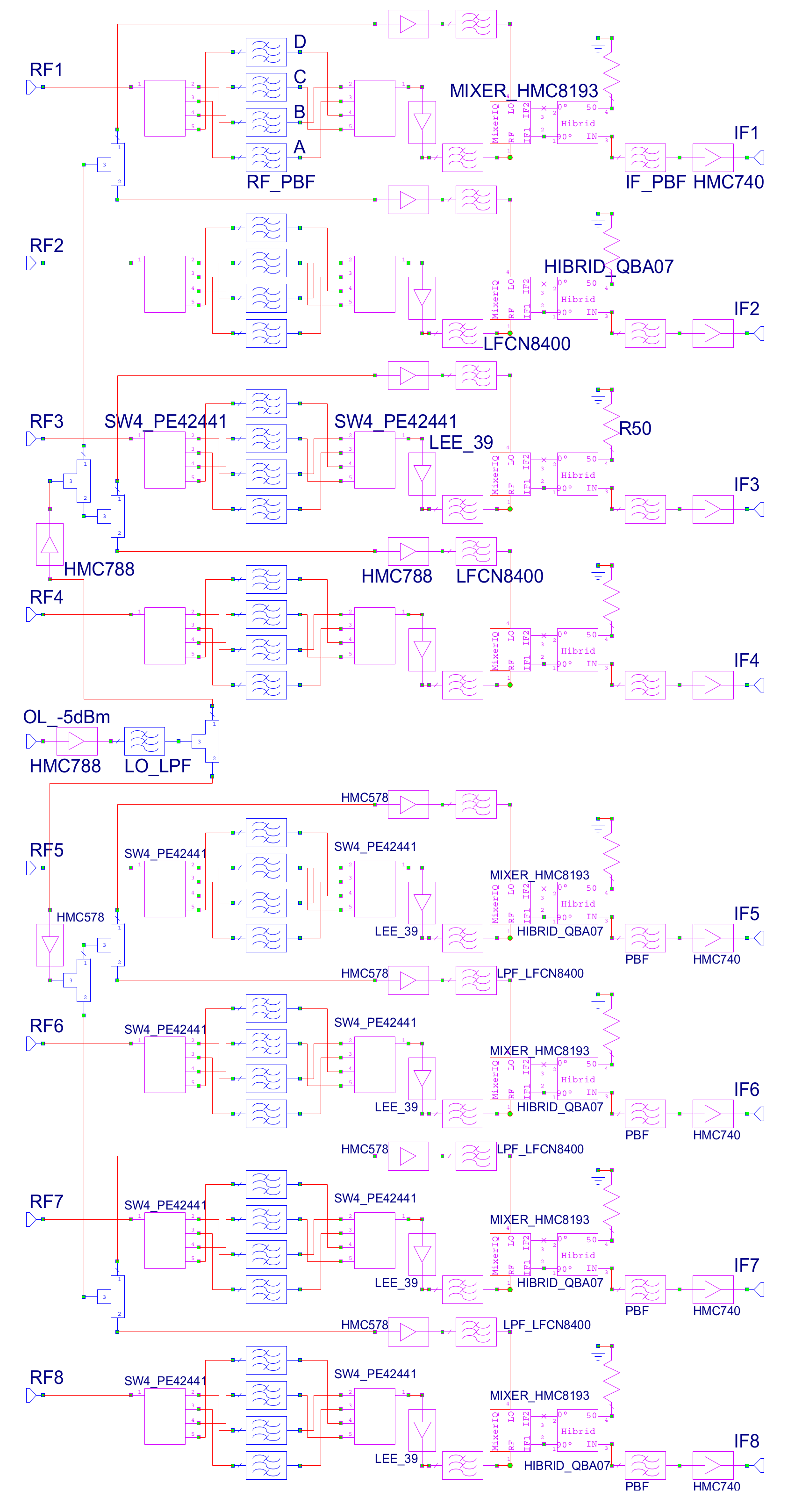
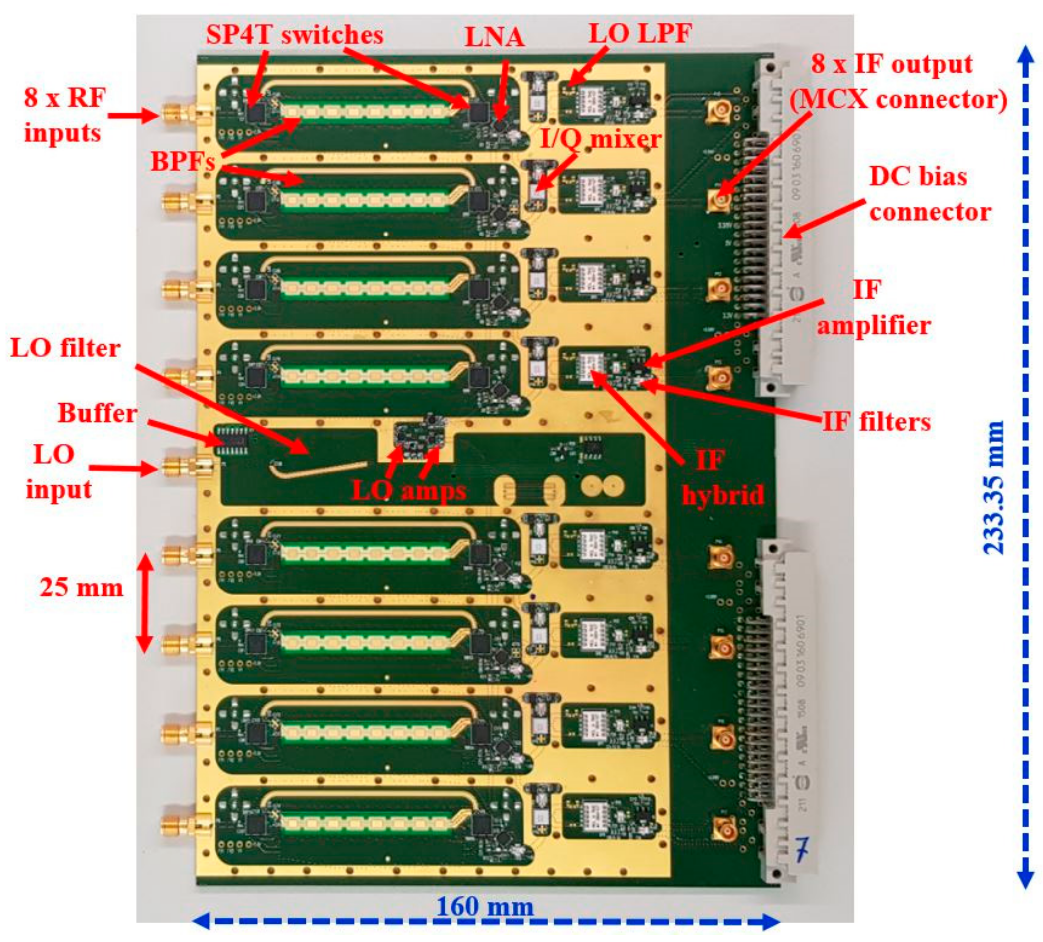
2.1. Eight-Channel Warm Section RF/IF Module

Each of the WS RF/IF modules (Figure 4) includes a PCB circuit and four WDM fiber-optic transmitters (OTXs) attached on opposite sides of a mechanical support. The RF/IF module has eight SMA (SubMiniature version A) RF input connectors, one SMA LO input connector centered on the front panel, and one quad LC/APC (Lucent Connector/Angle Polished Connector) output connector to extract the four WDM G652D IFoF optical fiber outputs provided by the four OTXs. Figure 5 shows a schematic of the receiver chain implemented on the board. The module employs a single four-layer PCB based on RG4003C (Rogers Corporation, Chandler, AZ, USA) substrate with a thickness of 0.508 mm and commercial surface-mounted components soldered in place (no bonding required).
The PCB adopts the standard double-height Eurocard size (6U) that can be plugged into a standard chassis which, in turn, can be mounted in a 19-inch rack. A cross-section view of the PCB (total thickness ≈ 1.76 mm, including substrates, prepegs and metallization) is shown in Figure 6. Metalized via holes are employed to connect the different metallization layers.
The board and its components (switches, RF and IF LNAs, mixers, etc.) are easy to fabricate and assemble. The board is biased with a single voltage (+5 V) and incorporates a sensor for monitoring the physical temperature. The IF output signals are extracted from micro coaxial connectors (MCX) mounted orthogonally to the board.
The eight channels of the board are based on identical components and same-length transmission lines in order to achieve identical performance: this was a design requirement that aimed at minimizing the amplitude and phase variations between the different WS receiver channels. These variations, if not properly minimized or calibrated out, affect the antenna beam patterns by causing their temporal modification. In fact, in a PAF the beams are formed by adding the responses of multiple elements. Thus, maintaining stable beams requires maintaining the same phases and amplitudes in all the receiver chains. By designing the WS with identical receiver channels, we minimized the potential phase and amplitude variations that could be caused by temperature gradients. In this respect, the mechanical support that holds the PCB helps mitigating these effects as it adds a thermal mass and minimizes thermal variations due to temperature changes that are external to the WS.
A 25 mm spacing between contiguous input SMA connectors allows accommodating nine uniformly distributed SMAs (eight RF plus a central one for the LO) on a 6U double-height Eurocard. Thus, the RF, IF and LO circuitries of each channel are required to be laterally confined within 25 mm. High electromagnetic isolation between the independent RF channels is provided by a series of uniformly spaced metalized via holes connecting the PCB layers, placed to surround the eight independent RF circuitries. All components are mounted on the PCB top metallization layer. The board is bolted with its top metallization layer in contact with the mechanical housing, designed to have rectangular pockets at positions that avoid interference with the PCB components. The pockets of the mechanical housing surround the independent circuitries of the PCB and provide extra electromagnetic isolation between the independent RF channels. Microwave absorbers are placed at the bottom of the pockets, above the components, to avoid cavity resonances (see next section).
A prototype version of the PCB was designed and fabricated. The prototype employs a BPF-A covering the 4–8 GHz band, rather than the 2.3–8.2 GHz band of the “production” board presented in this paper. Views of two of the production board PCB layers are shown in Figure 7. BPF-A is based on a L-C cell high-pass filter cascaded with a microstrip eight-pole Chebyshev low-pass filter, while BPF-B, C and D are based on six-pole Chebyshev bandpass filters fully implemented on microstrip. Due to their narrow-band features BPF-B, C and D could be optimized for low input reflection and insertion loss, while BPF-A resulted in more limited performance due to its broadband characteristics.
The four-way switch filter-bank allows selection of one of the four RF band pass filters through two SP4T switches (Peregrine PE42441). An inverting buffer (TI SN7404) is used to route the DC signals to bias the switches. The switches are configured to enable selection of the same filter type in all channels of the four WS RF/IF modules at the same time through a two bit TTL signal. Figure 8 shows the detail of a part of the circuit board centered around one of the switch filter bank section. The switched filter-bank is cascaded with an RF amplification stage followed by a sideband separating (2SB) mixer (see Figure 2 and Figure 5) operated in single down conversion LSB mode. The 2SB mixer consists of a commercial I/Q mixer (AD HMC8193) cascaded with a 90° IF hybrid (mini-circuits QBA-07+) that delivers two IF output signals to two independent ports. The USB output of the IF hybrid is terminated into a 50 Ω load, while its LSB output is band pass filtered and amplified. The IFs signal are routed to the on-board MCX connectors. Eight 16.5 cm long coaxial cables (type RG316), connectorized with male MCX connectors on both sides, are employed to transport the IF signals from the board to the input of the WDM fiber-optics transmitters, each of which accepts two IF inputs. The OTXs are mounted on the backside of the mechanical support that houses the PCB (see Figure 4a).
The PCB has one SMA connector for the LO input signal, centrally located on the RF side of the board. The LO signal is amplified, band pass filtered (by a cascade of low pass and high pass filters) and distributed internally to the I/Q mixers of the PCB with one eight-way splitter based on a cascade of Wilkinson power dividers. Equal electrical path lengths are used for the LO distribution signal chain to the eight receiver channels of the PCB. Each mixer is pumped with a LO power of ≈ 18 dBm and has a typical image rejection of 25 dBc. The LO power level required at the LO coaxial connector of each of the WS RF/IF modules is ≈−5 dBm.
We used the commercial software NI-AWR Microwave Office to design the PCB circuitry and simulate the electromagnetic response of the WS receiver chains with their band pass filters and components. The S-parameter simulator was employed to optimize the scattering parameters of the receiver chains. We imported the S parameters of the components (available from the manufacturers website) in the electromagnetic simulation program and optimized the parameters of the interconnecting transmission lines and matching circuitries.
Figure 9 plots the simulated RF transmissions that would be obtained by selecting the four BPFs. The simulated response of the filters closely matches the specified ones in terms of passband (bandwidth at half-power points), insertion loss, return loss, in-band ripple, stop-band attenuations, and size.

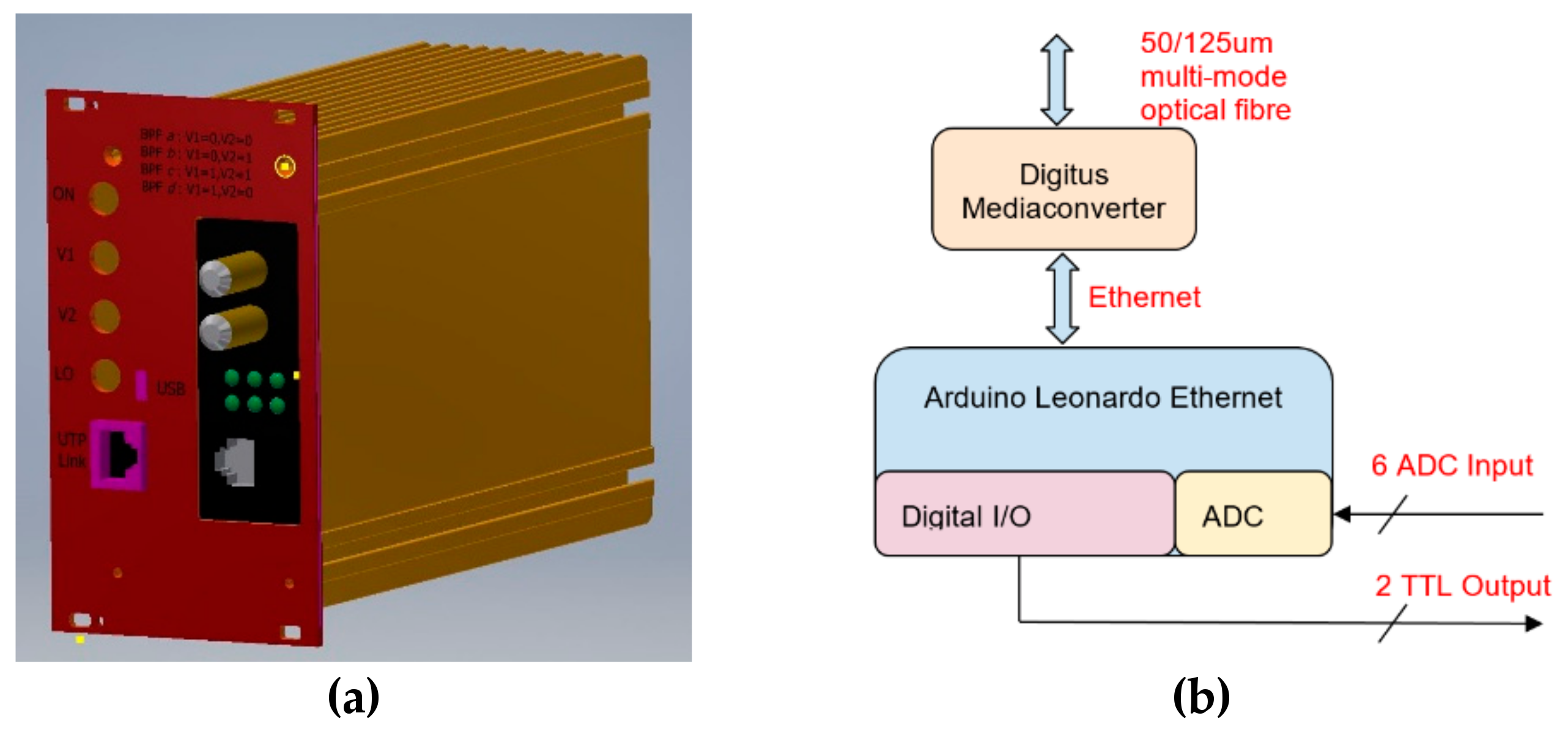
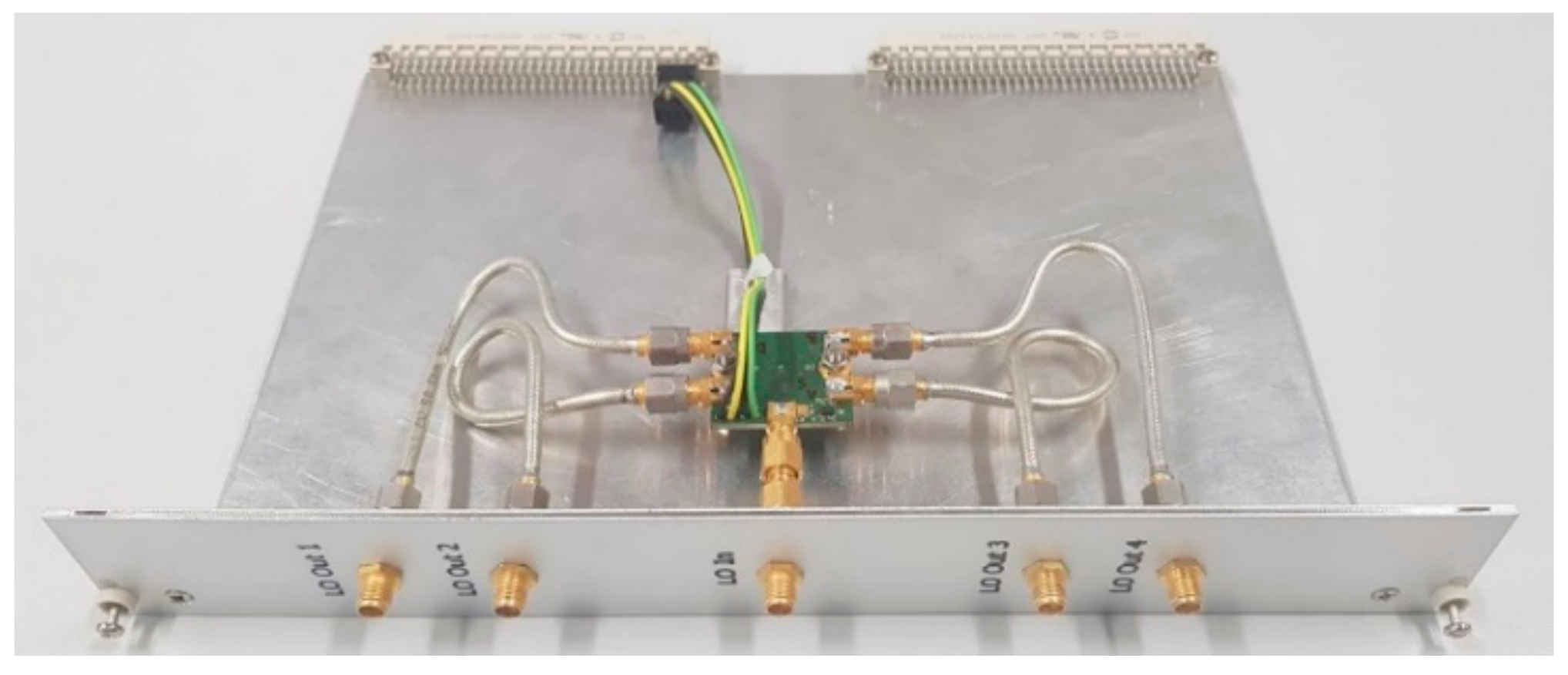
2.2. Local Oscillator Distribution Module

The four WS RF/IF modules receive a copy of the same LO signal from the LO distribution module (Figure 3) so that the 4 × 8 mixers are pumped under identical conditions. The design of the 2.950–8.575 GHz four-way LO splitter, based on Wilkinson power dividers implemented on the Rogers RG4003C substrate, is shown in Figure 10. The LO splitter board incorporates a directional coupler (coupling value ≈ −20 dB) that directs part of the signal to a detector (AD8317, Analog Devices Corporate, Norwood, MA, USA). The detector converts the LO power to a decibel-scaled DC output. The DC voltage, inversely proportional to the LO power, is used for monitoring purposes. The power level at the SMA input of the LO distribution module should be ≈+5 dBm in order to have ≈−5 dBm at the SMA LO input connector of the WS RF/IF modules.

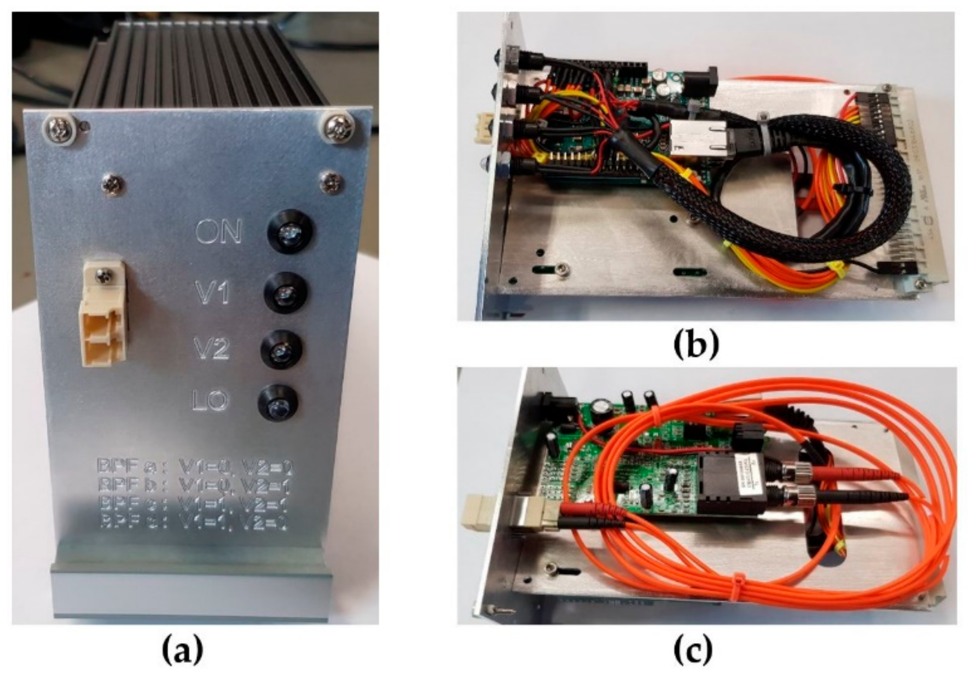
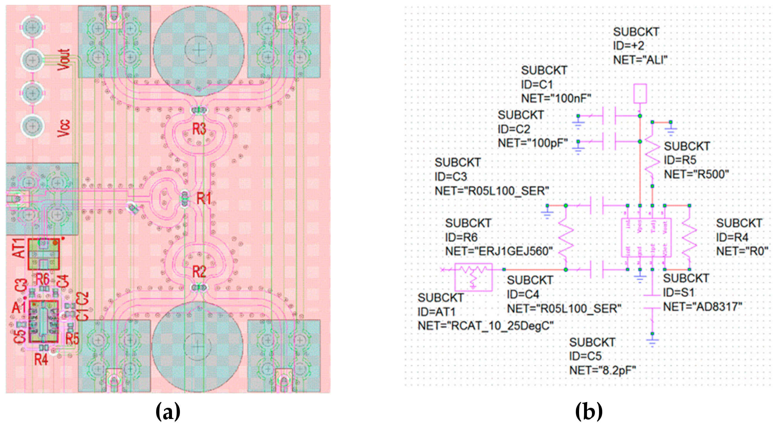
2.3. Warm Section Monitor and Control Module

The WS monitor and control (M and C) module (Figure 3 and Figure 11) is based on a commercial optical fiber to Ethernet media-converter (Digitus DN-82010, Lüdenscheid, Germany) and microcontroller (Arduino Leonardo ETH) incorporated into a 3U rack-mountable box biased with +5 V. The module utilizes a transmitting/receiving mode with a TX/RX multimode fiber and has two TTL outputs. It allows the selection of one among four possible BPFs and returns voltage values that are inversely proportional to the LO power of the LO distribution module. Furthermore, the module reads the physical temperature provided by four sensors (one per PCB). The front-panel includes LEDs for visual information on the selected filter, the presence/absence of LO power (set to switch the led off if power is below a given threshold) and of bias voltage.

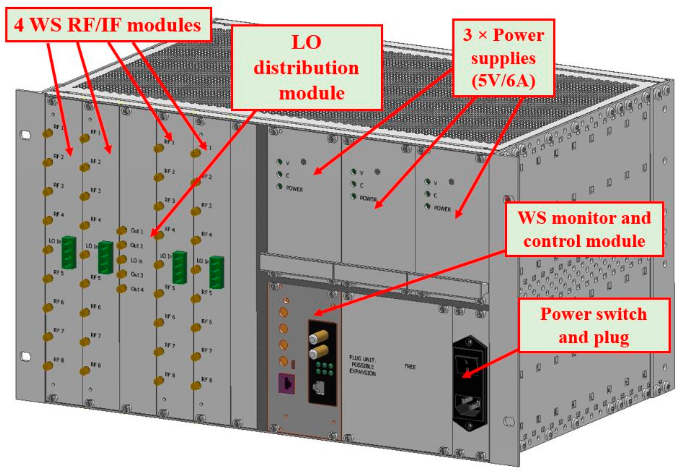
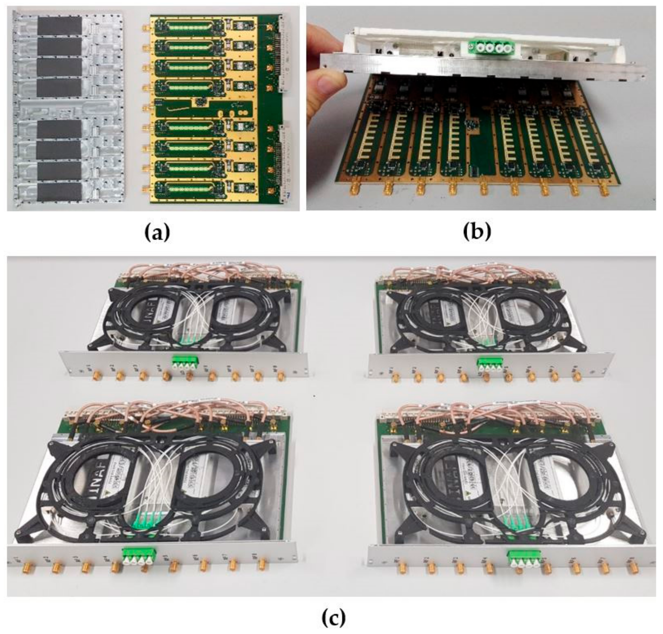
3. WS Fabrication, Integration and Assembly

In this section we describe the fabrication of the PCBs and their integration and assembly with the other components that form the WS RF/IF modules. Also, we illustrate the assembly of the LO distribution module and of the monitor and control module. Then, we present how all these modules are assembled into racks.

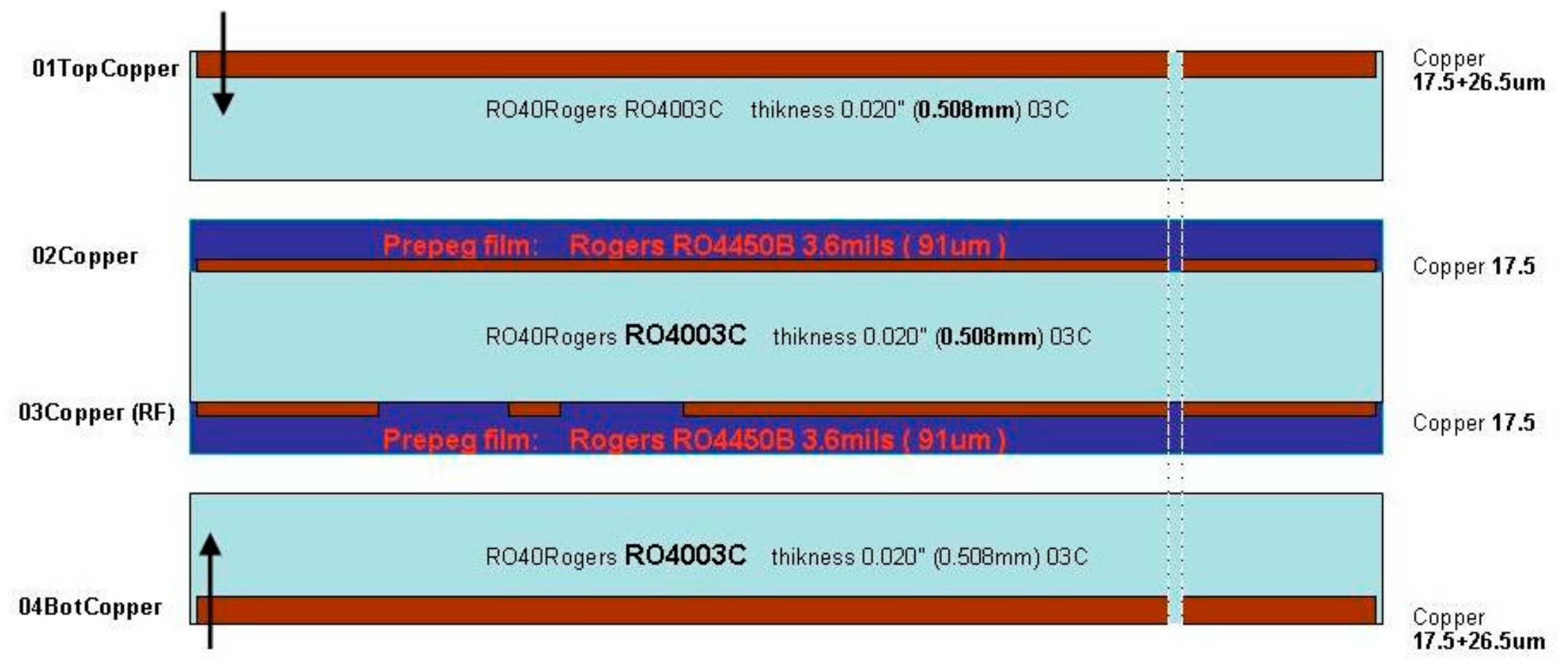
3.1. Eight-Channel Warm Section RF/IF Module

The WS RF/IF board was fabricated and assembled by two Italian companies. A photo of one of the boards is shown in Figure 12. The board includes the SMA input connectors, the MCX output connectors and two 96-pin DC connectors (DIN 41612C, Deutsches Institut für Normung, Berlin, Germany). The DC bias connector visible on the top right of Figure 12 is used for biasing, controlling and monitoring, while the one on the bottom right only serves mechanical purposes such as better fixing of the board to the standard chassis backplane of the rack.
The PCB mechanical housings were fabricated by INAF. Figure 13 shows photos of the boards we fully assembled with the mechanical housing and optical transmitters. The four OTXs of each module are fixed to the mechanical housing that supports a plastic frame used for routing the optical fibers to the quad LC/APC connector.
The IFoF fiber-optic links were developed for the SKA low frequency aperture array by an INAF‑led collaboration with industrial partners and adopted for this project. The test results of the ones adopted for PHAROS2 are given in reference [15]. The WDM IF over fiber technology utilizes dual distributed feedback (DFB) laser sources on the OTXs and dual photodiode detectors on the ORXs, thereby providing IF isolation between channels greater than 45 dB up to the maximum frequency (650 MHz). The signals are de-multiplexed at the optical receiver side. The optical (infrared) wavelengths at λ = 1270 nm and λ = 1330 nm were chosen to minimize the signal dispersion of the G652D optical fibers across the IF band. The OTX optical lasers are class 3A, delivering an optical power at each of the two WDM wavelengths of less than 5 mW (total of the optical power less than 10 mW per link). The length of the optical-fiber pigtail from the transmitter to PHAROS2 WS RF/IF board is 1 m. The ORX utilizes two independent IF receiver chains that adapt the signals for digital conversion by the following iTPM analog to digital unit (ADU). Each of the chains perform amplification and level adjustment through digital step attenuators (DSAs) with 31 dB range and 1 dB step. The OTX control adopts the SPI bus from the ADU board. The maximum gain of the IFoF link is ≈60 dB when the DSA is set to its minimum attenuation of 0 dB (the link gain is of order ≈ 35 dB when setting the DSA to 25 dB).
Each optical transmitter absorbs a current of 200 mA and is biased from the PCB with a voltage of 5 V through the central pin of one of the two input MCX connectors (total power consumption of order 1 W per OTX). The power consumption of one WS RF/IF module, 12.5 W (2.5 A × 5 V), is due to the four OTXs (≈4 W) and the PCB board (≈8.5 W).

3.2. LO Distribution Module

The LO distribution board was fabricated on the same PCB fabrication run as the RF/IF boards. The four-way LO splitter PCB is mounted on a thin aluminum frame that supports two DIN DC connectors on the backplane side for bias and monitor of the LO. Coaxial cables are used to connect the board to the module front-panel (see Figure 14).

3.3. Monitor and Control Module

We developed two versions of the M and C module. The first version employed the Digitus media-converter on the front panel (as from drawing of Figure 11). In the new version, the media-converter is located inside the mechanical box for better screening of the self-generated RFIs, as shown in Figure 15.

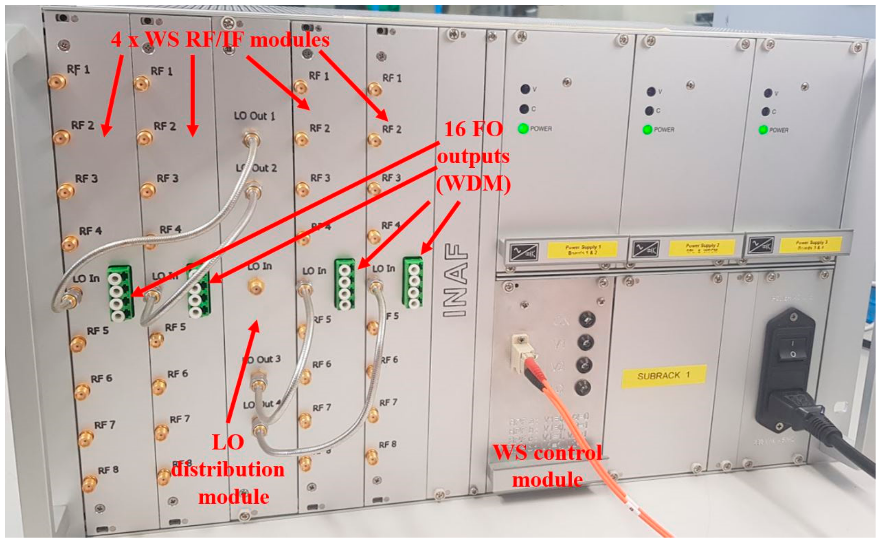
3.4. Fully Assembled 32-Channel Receiver

Two identical 32-channel receivers were fully assembled and characterized, although only one was required to equip the PHAROS2 PAF. In total, eight WS RF/IF modules (four per rack), two LO distribution modules and two M and C control modules were built and tested.
Figure 16 shows a photo of one of the two 32-channel receivers assembled at INAF. The four RF/IF modules, the LO distribution module and the M and C module are arranged in the standard 19-inch rack that also includes three 3U commercial linear power supplies (Schroff PSG105, Straubenhardt, Germany, 5V/6A each) and a module for the 230 VAC plug and switch on the front panel. All the connections and DC distribution are implemented on the rack backplane. The four WS RF/IF modules a total power consumption of ≈50 W (see Section 3.1). We measured the power consumption of the fully assembled WS rack to be ≈140 W. This value accounts for the consumption of the four WS RF/IF modules, of the three linear power supplies (efficiencies less than 50%-not used at their maximum ratings), of the control module and of the LO distribution module.

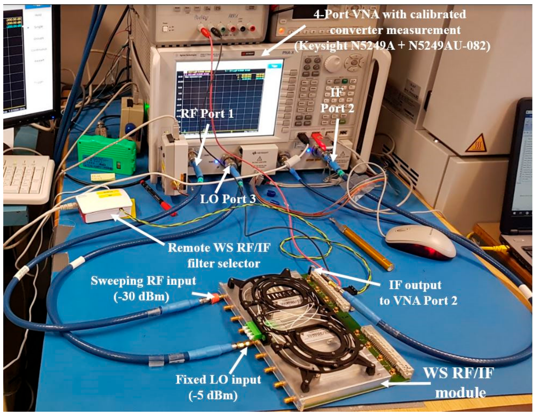
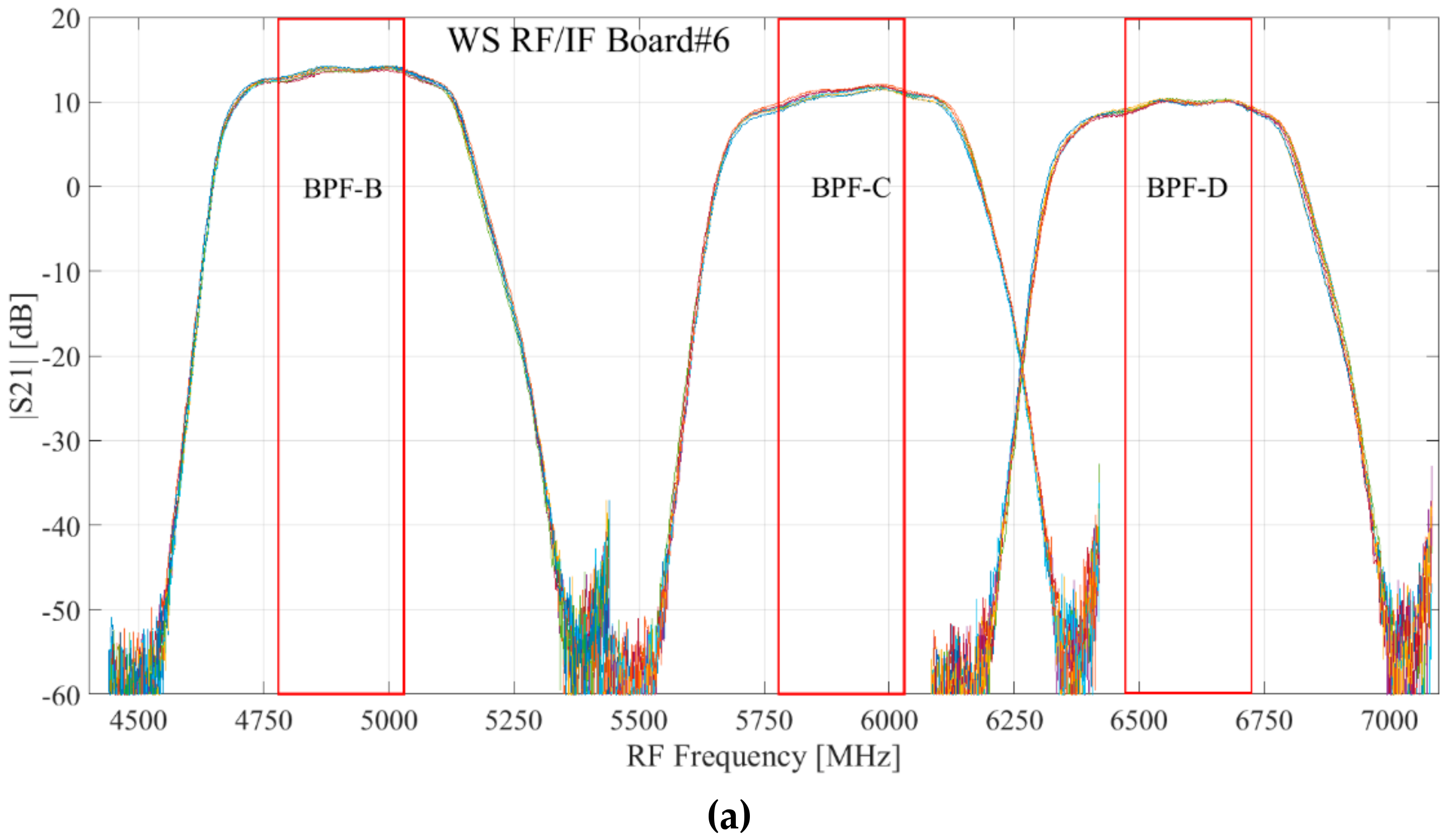
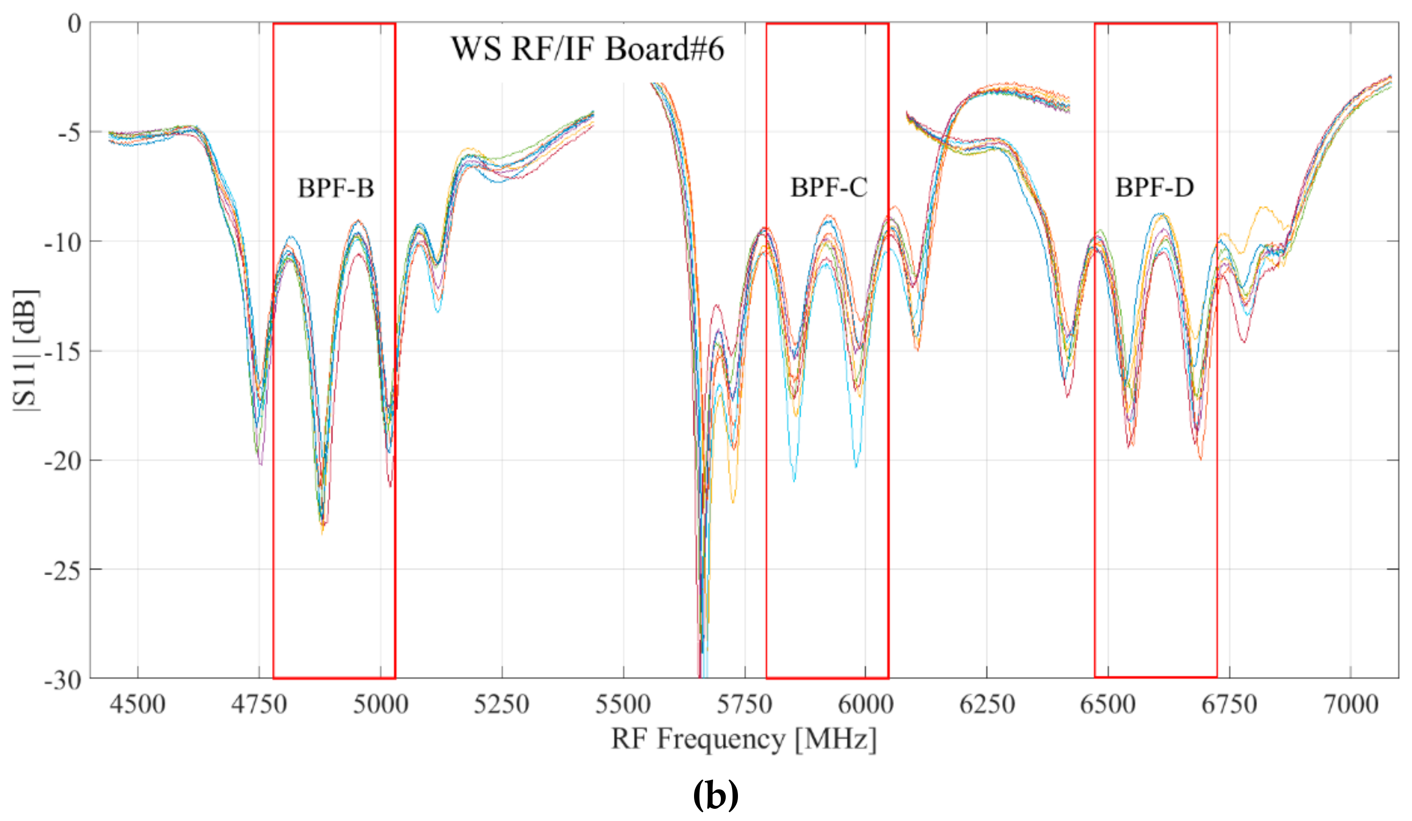
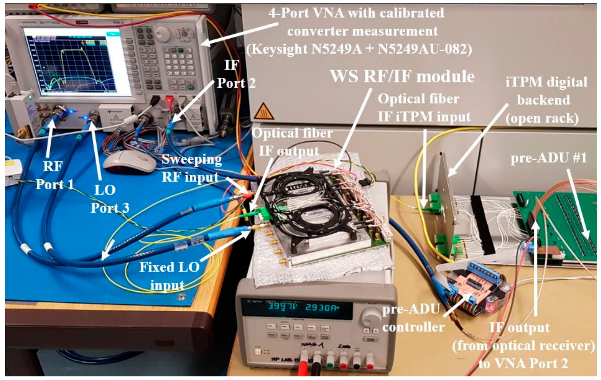
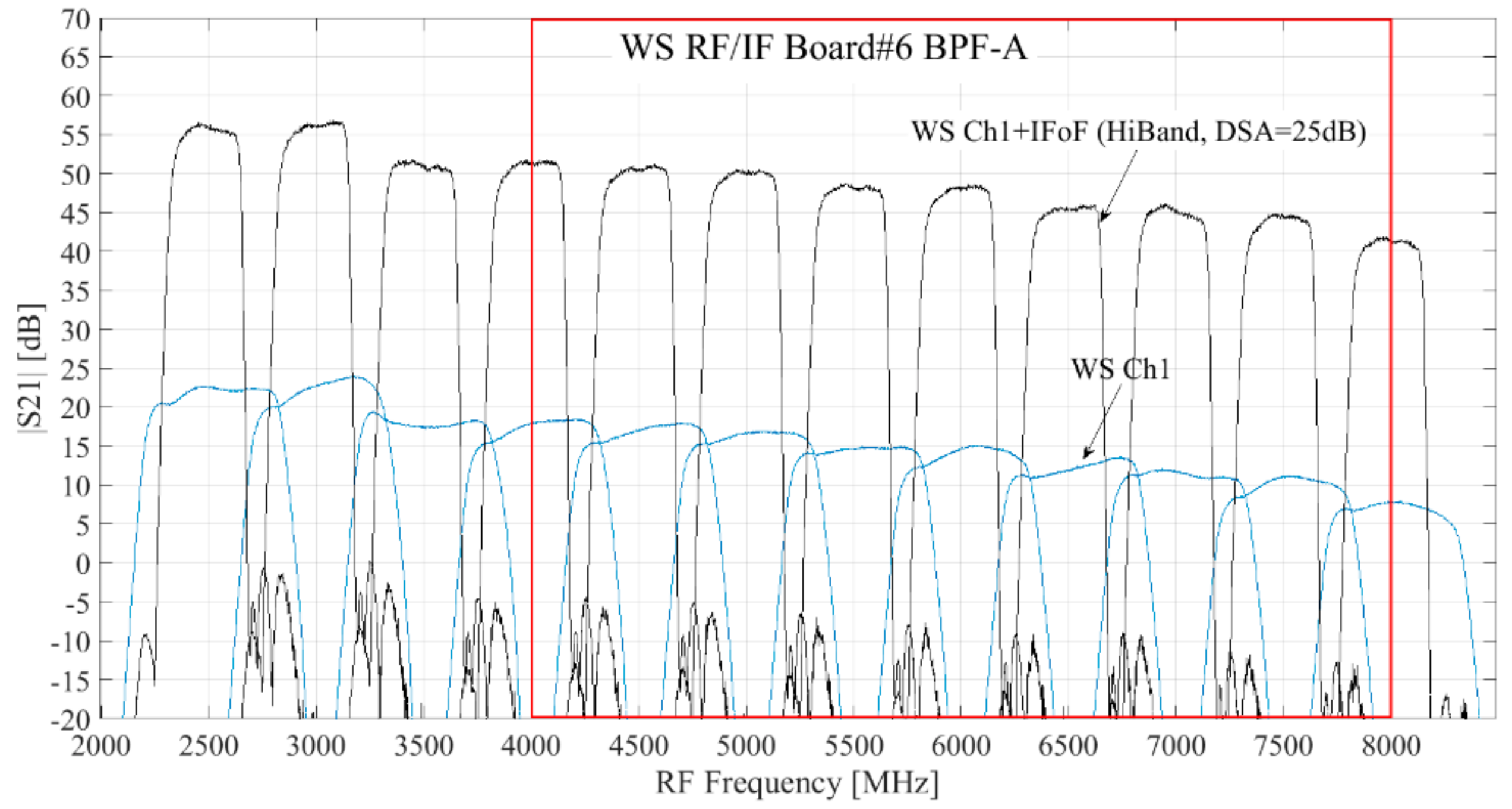
4. WS Multi-Channel Receiver Characterization

We characterized the eight-channel WS RF/IF modules before assembling them in the two receiver racks. For the tests, we utilized a 4-port VNA (vector network analyzer) equipped with calibrated converter measurement capabilities (Keysight N5249A and N5249AU-082, Keysight Technologies, Inc., Santa Rosa, CA, USA). We calibrated out the effects of the coaxial cables from the VNA ports to the WS RF/IF module ports. We developed a MATLAB script for automatic data acquisition, processing and analysis of the WS boards’ VNA test results.
The modules perform well according to their specifications and have similar performances. Below, we present the characterization results of one of them (Board #6). We tested the modules in two situations:
  • Without the IFoF optical links, by extracting the IF outputs from the on-board MCX IF connectors;
  • Including the IFoF optical links, by extracting the IF after optical-to-IF conversion using the iTPM pre-ADUs digital backend.

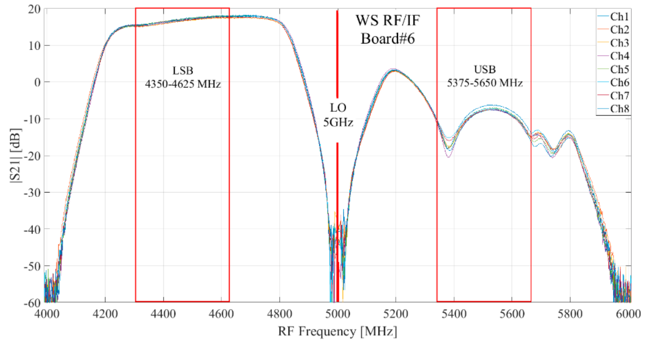
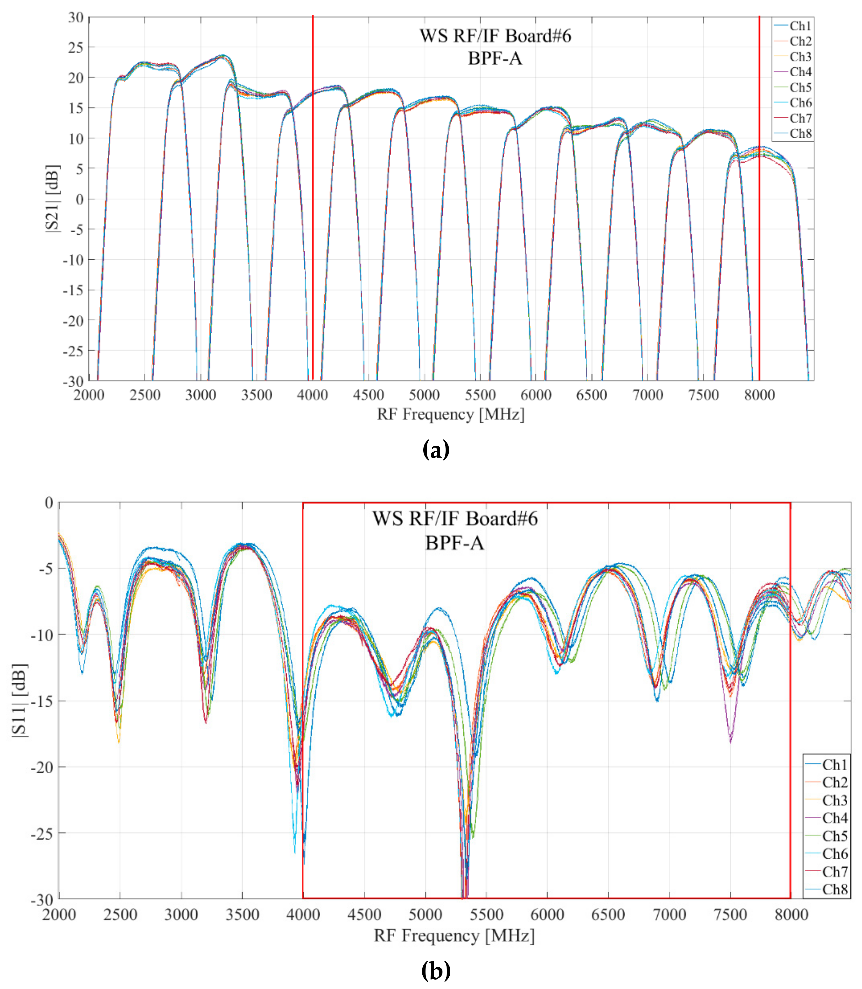
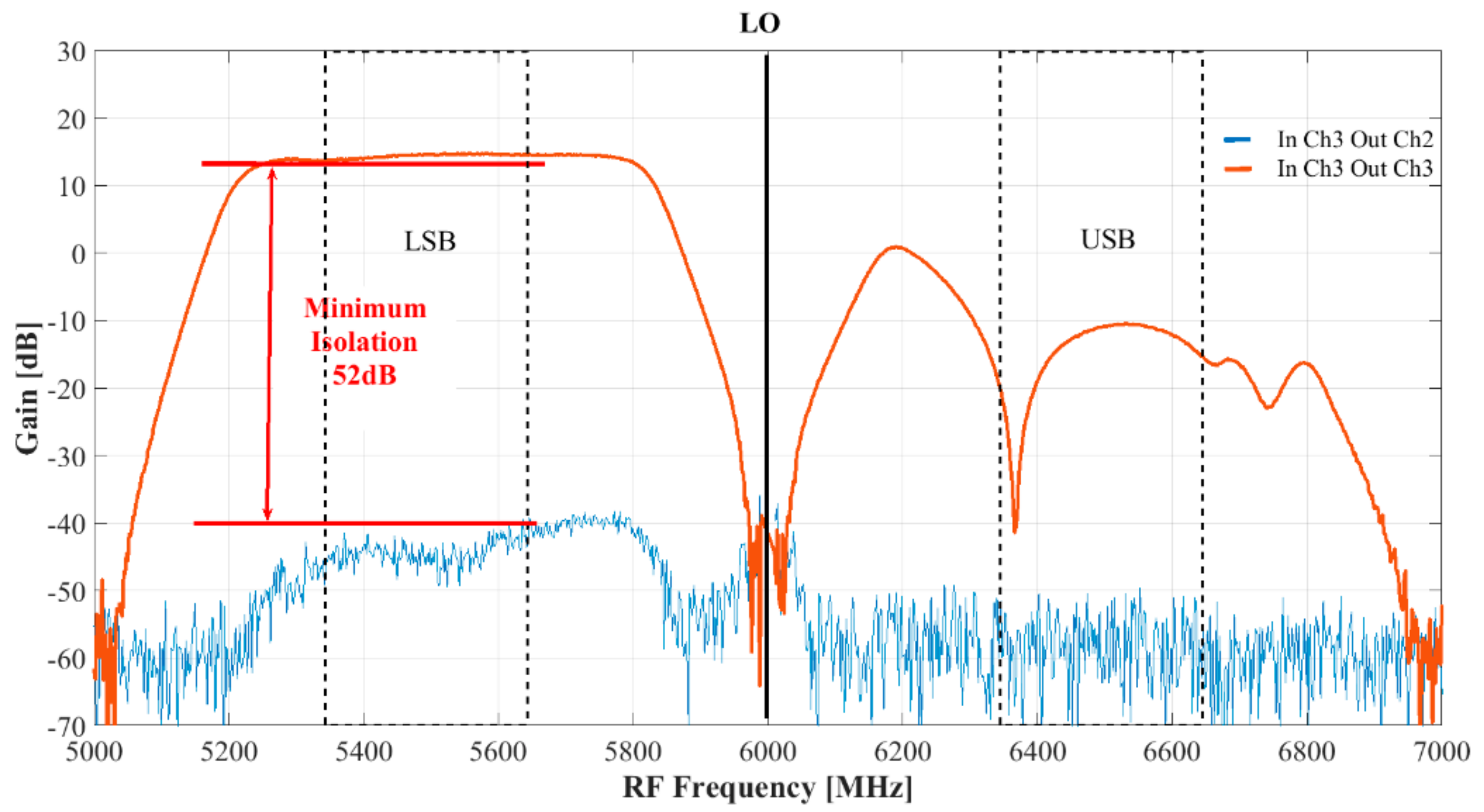
4.1. Characterization of Eight-Channel WS RF/IF Modules without IFoF Links

The test setup is shown in Figure 17. We connected VNA Port 3 to the board SMA local oscillator input, and VNA Ports 1 and 2, to the SMA RF input connector and to the MCX IF output connector, respectively. The powers at the board inputs were set to −5 dBm on the LO port and to −30 dBm on the RF port, respectively. We tested the eight channels in turn, one after the other.
Figure 18 shows an example of the measured receiver gains for the eight channels when the LO is set at a fixed frequency of 5 GHz and the RF is swept from 4 GHz to 6 GHz, with broadband band pass filter “BPF-A” selected. Vertical lines (in red) limit the nominal LSB (5350–4625 MHz) and USB (5375–5650 MHz) that are down-converted to the 375–650 MHz IF band. All channels show very similar responses. The receiver gain is in the range 15–18 dB across the LSB (signal band) and below −6 dB across the USB (image band). The image sideband rejection, i.e., the ratio between the conversion power gains GLSB/GUSB at the IF port, depends on LO and IF frequencies. For the given LO frequency the rejection has a minimum of ≈23 dBc around the center of the IF band (≈510 MHz) and reaches values greater than 40 dBc towards the IF band edges. We repeated the above tests for 12 different LO frequencies, from 3 GHz to 8.5 GHz by 0.5 GHz steps (signal frequencies from 2.35 GHz to 8.125 GHz). The measured results for the LSB gains of the eight board channels, added together in a single graph, are shown in the top panel of Figure 19 (the USB responses are not plotted for better clarity). The envelope of the LSB gains are in the range 6–23 dB. The gains are greater towards the lower part of the RF band (around 2.5 GHz) and decrease at the highest frequencies (around 8 GHz). The two vertical lines at 4 GHz and 8 GHz delimit the nominal RF band edges of the PHAROS2 PAF. The plots of Figure 19 show that the receiver performs well across the 2.3–8.2 GHz band and that the eight channels of the board have very similar performance. The greatest gain differences are measured towards the highest RF frequencies, where the channel-to-channel variations reach values of order 3 dB. The image sideband rejection is greater than ≈23 dBc at all LO frequencies. For all LO tested values, the rejections versus IF frequency show very similar responses: the rejection has minima in the range 20–30 dBc that always fall around the IF band center (≈510 MHz) and reach values greater than 40 dBc (up to 60 dBc) towards the IF band edges (at 375 MHz and 650 MHz). This result indicates that, for a given observation across the 275 MHz instantaneous IF band of a narrow-band radio astronomy signal (in LSB) with BPF-A it might be possible to adjust the LO frequency to maximize the rejection of an unwanted interferer (for example a Radio Frequency Interference) occurring in the image band.
The bottom panel of Figure 19 shows the reflection coefficient measured at the RF input connectors of the board. |S11| is less than −3 dB across 2.3–8.2 GHz and less than −5 dB across 4–8 GHz.
We characterized the channel-to-channel isolation of the fully assembled module at various LO frequencies.
Figure 20 shows the measured transmissions (for LO frequency set 6 GHz) when injecting the RF signal from the VNA port into channel 3 and extracting the IF outputs from:
  • The MCX connector of channel 3 (brown curve, resulting in a channel 3 gain of order 13 dB);
  • The MCX connector of channel 2 (blue curve).
The measured channel-to-channel isolation is greater than 52 dB at the selected LO frequency. We repeated the same measurement at other LO frequencies, using different channel combinations and different boards. Although the isolation slightly deteriorates when measuring contiguous channels of the board (i.e., channel 2 and channel 3, or channel 3 and channel 4, etc.), as compared to non-contiguous channels (for example channel 1 and channel 7), we found that the channel-to-channel isolation is always greater than 45 dB at all frequencies across 2.3–8.2 GHz for all the WS RF/IF boards. We tested the channel-to-channel isolation of the board without the mechanical housing and found very little deterioration on the isolation performance.
The cumulated S-parameter test results of the eight channels of board #6, when the three narrow band filters are selected in turn, are shown in Figure 21. The top panel plots the measured transmissions for the three respective LO frequencies. All channels have very similar responses, with gains of 10 dB. The image sideband rejection GLSB/GUSB is greater than 50 dBc for any IF frequency across the 375–650 MHz. This high rejection value results from the combined effect of the mixer sideband separation and of the filter rejection. The bottom panel of Figure 21 shows the cumulated reflection measured at the RF input connectors. The values are below −8 dB across the nominal bands of the three filters. Figure 19 and Figure 21 show different variations across the band for both insertion loss and return loss for the wideband filter BPF-A and the “narrow-band” filters BPF-B, C and D. In particular, the narrow-band filters show a much better response with lower reflection and flatter band pass, as expected from the electromagnetic simulations. The inferior response of BPF-A (maximum input reflection of order −5 dB around 6.6 GHz) is expected to generate low standing wave value on the receiver chain because such a filter will be connected (through coaxial cables) to the PHAROS2 cryogenic LNA that has a well matched 50 Ω output.

4.2. Characterization of Eight-Channel WS RF/IF Modules with IFoF Links

The test setup we adopted for characterizing the RF/IF modules with IFoF transmitters is similar to the one that was presented previously, except that Port 2 of the VNA is this time connected to the MCX IF output of the ORX, which is part of the pre-ADU, the analog section of the iTPM digital backend [12]. Therefore, the IF signal is extracted after the signal conditioning and amplification operated by the IFoF fiber optic link. The setup is shown in Figure 22. The digital step attenuators (DSA) of the IFoF link were set to 25 dB, so that the link total gain was approximately 30–35 dB. The test results for the receiver gain for one of the channels of the WS RF/IF module (channel 1 of board #6) with the optical link is shown in Figure 23. The plot cumulates the results for 12 different LO frequency settings. For comparison, the measured receiver gains of the WS RF/IF board (with no IFoF link) is also plotted on the same figure. The WS receiver with IFoF link has an average gain across the PHAROS2 4–8 GHz band of ≈50 dB with DSA set to 25 dB and can be varied from ≈45 dB to ≈75 dB by changing the DSA from 31 dB to its 0 dB minimum attenuation. For comparison, the fixed gain of the WS receiver without IFoF link has an average of ≈15 dB (in the range ≈8–18 dB across 4–8 GHz).

5. Conclusions

We presented the development of a 32-channel room temperature heterodyne receiver for the PHAROS2 (phased arrays for reflector observing systems 2) phased array feed (PAF). The receiver is the signal chain section located between the cryogenically cooled PAF antenna array and the digital beamformer that will enable first-ever radio astronomy observation in C-band with a PAF. The receiver is based on four eight-channel radio frequency (RF)/intermediate frequency (IF) modules that in total are capable of processing 32 × RF signals across the 2.3–8.2 GHz frequency range. A switched filter bank is located at the input of each of the channel, enabling us to select one out of four possible bandpass filters: either a wide-band filter (BPF-A) or one of three narrow-band filters (BPF-B, C and D) centered around astronomical lines. The receiver chains are based on sideband separating I/Q mixers operating in the lower sideband (LSB), with the upper sideband (USB) being internally terminated. The mixer 375–650 MHz IF outputs (275 MHz band), following IF amplification and filtering, are converted to optical by analogue wavelength division multiplexing laser transmitting modules integrated into the Warm Section (WS) receiver rack. The WS outputs are four quad LC/APC fiber-optics connectors delivering a total of 32 × IF analogue fiber-optics signals (two IF signals per fibers). In PHAROS2, such optical signals will be transported (through optical fibers) to the Italian tile processing module (iTPM) for conversion back to IF by the optical receivers located into the pre-ADUs (pre-analog to digital units).
The test results show that the two WS 32-channel receivers we built, one of which will be used for PHAROS2, perform well and according to specification. The 2.3–8.2 GHz signal frequency band can be covered with multiple local oscillator (LO) tuning by selecting filter BPF-A. The LSB signal gains (GLSB) and image sideband rejections (IR) of the WS receiver modules without optical link across 2.3–8.2 GHz are in the range GLSB = 6–23 dB and IR = 23–60 dBc, respectively. Within the 275 MHz band covered by the receivers, the gain variation is ±2.5 dB around the average value. The image sideband rejection with BPF-A has minima ≈ 20 dBc at the center of the IF band (≈510 MHz).
Selection of one of the narrow band filters BPF-B, C or D (≈300 MHz bandwidth) allows us to operate the receiver channels with much improved performance: the lower side band (LSB) signal gains and image sideband rejections of the WS receiver modules without optical link are in the range GLSB = 9–13 dB and IR > 50 dBc, respectively. Within the 275 MHz band covered by the receivers the gain variation is ±1 dB around the average value.
Few WS multi-channel receivers could be used in parallel to process multiples of 32 × RF input signals. For example, six WS receiver racks could be arranged in a standard cabinet (19-inch wide, 36U in height) to process 96 pre-amplified input signals from a 2.3–8.2 GHz dual-polarization PAF that is capable of forming few tens of synthesized beams on a radio astronomy antenna.

Author Contributions

A.N., A.S. (Alessandro Scalambra), P.O., F.P., A.M. and A.C. defined the system architecture. A.S. (Alessandro Scalambra) performed the electromagnetic design of the PCB., A.N. acquired the funds for receiver’s construction, procured the parts through the INAF purchasing department, and performed the project administration. J.R. and P.M. designed and fabricated the receiver mechanical parts. P.O. and A.S. (Andrea Saba) developed the receiver monitor and control module and the control software. M.P. assembled the racks and wired the backplane that host the receiver modules. S.R. developed the MATLAB script for automatic data acquisition, processing and analysis of the WS boards VNA test results. A.S. (Alessandro Scalambra), S.R., A.N., A.L. and L.S. performed the assembly and characterization of the receiver. A.N., A.S. (Alessandro Scalambra) and S.R. performed the analysis of the measured results and the data curation. A.N. prepared the article draft. All authors reviewed the article.

Funding

This research was funded by INAF (National Institute for Astrophysics)-Scientific Directorate, “Industrial Astronomy SKA 2017”, Ob.Fu. 1.05.03.37.03.

Acknowledgments

We thank J. Monari, M. Morsiani, A. Mattana and M. Schiaffino of the INAF-Institute of Radio Astronomy, Italy, for their advices and for providing support during the project definition and assembly of the receivers. We thank the international partners of the PHAROS2 SKA PAF Advanced Instrumentation Program consortium for helpful discussion.

Conflicts of Interest

The authors declare no conflict of interest.

References

  1. Fisher, J.R.; Bradely, R.F. Full-sampling array feeds for radio telescopes. In Proceedings of the SPIE Astronomical Telescopes and Instrumentation, Munich, Germany, 3 July 2000. [Google Scholar]
  2. Warnick, K.; Maaskant, R.; Ivashina, M.V.; Davidson, D.B.; Jeffs, B.D. High-Sensitivity Phased Array Receivers for Radio Astronomy. Proc. IEEE 2016, 104, 607–622. [Google Scholar] [CrossRef]
  3. Anish Roshi, D.; Shillue, W.; Simon, B.; Warnick, K.F.; Jeffs, B.; Pisano, D.J.; Prestage, R.; White, S.; Fisher, J.R.; Morgan, M.; et al. Performance of a highly sensitive, 19-element, dual-polarization, cryogenic L-band phased array feed on the Green Bank Telescope. Astron. J. 2018, 155, 18. [Google Scholar]
  4. DeBoer, D.R.; Gough, R.G.; Bunton, J.D.; Cornwell, T.J.; Beresford, R.J.; Johnston, S.; Feain, I.J.; Schinckel, A.E.; Jackson, C.A.; Kesteven, M.J.; et al. Australian SKA Pathfinder: A High-Dynamic Range Wide-Field of View Survey Telescope. Proc. IEEE 2009, 97, 1507–1521. [Google Scholar] [CrossRef]
  5. Hut, B.; van den Brink, R.H.; van Cappellen, W.A. Status update on the system validation of APERITIF, the phased array feed system for the Westerbork synthesis radio telescope. In Proceedings of the 11th European Conference on Antenna and Propagation (EUCAP), Paris, France, 19–24 March 2017. [Google Scholar]
  6. Simons, J.; Ivashina, M.; Vaate, J.G.B.D.; Roddis, N. Beamformer system model of focal plane arrays in deep dish radio telescopes. In Proceedings of the European Microwave Conference, Paris, France, 4–6 October 2005; Volume 3, p. 4. [Google Scholar]
  7. Ciccognani, W.; Di Paolo, F.; Giannini, F.; Limiti, E.; Longhi, P.E.; Serino, A. A GaAs Front-end Receiver for Radio Astronomy Applications. In Proceedings of the 13th IEEE Melecon, Malaga, Spain, 16–19 May 2006. [Google Scholar]
  8. Liu, L.; Grainge, K. Realization of phased arrays for reflector observing systems. In Proceedings of the XXXIInd General Assembly and Scientific Symposium of the International Union of Radio Science (URSI GASS), Montreal, QC, Canada, 19–27 August 2017. [Google Scholar]
  9. Liu, L.; Grainge, K.; Navarrini, A. Analysis of Vivaldi array antenna for phased array feeds application. In Proceedings of the IEEE MTT-S International Conference on Numerical Electromagnetic and Multiphysics Modeling and Optimization for RF, Microwave, and Terahertz Applications (NEMO), Seville, Spain, 17–19 May 2017. [Google Scholar]
  10. Navarrini, A.; Monari, J.; Scalambra, A.; Melis, A.; Concu, R.; Naldi, G.; Maccaferri, A.; Cattani, A.; Ortu, P.; Roda, J.; et al. Design of PHAROS2 Phased Array Feed. In Proceedings of the 2nd URSI Atlantic Radio Science Meeting (AT-RASC), Gran Canaria, Spain, 28 May–1 June 2018. [Google Scholar]
  11. Van Ardenne, A.; Bregman, J.D.; van Cappellen, W.A.; Kant, G.W.; Bij de Vaate, J.G. Extending the Field of View with Phased Array Techniques: Results of European SKA Research. Proc. IEEE 2009, 97, 1531–1542. [Google Scholar] [CrossRef]
  12. Naldi, G.; Comoretto, G.; Chiello, R.; Pastore, S.; Pupillo, G.; Mattana, A.; Melis, A.; Concu, R.; Alderighi, M.; Aminaei, A.; et al. Development of a new digital signal processing platform for the Square Kilometer Array. In Proceedings of the 2nd URSI Atlantic Radio Science Meeting (AT-RASC), Gran Canaria, Spain, 28 May–1 June 2018. [Google Scholar]
  13. Vaz, B.; Verbruggen, B.; Erdmann, C.; Collins, D.; Mcgrath, J.; Boumaalif, A.; Cullen, E.; Walsh, D.; Morgado, A.; Mesadri, C.; et al. A 13Bit 5GS/S ADC with Time-Interleaved Chopping Calibration in 16NM FinFET. In Proceedings of the IEEE Symposium on VLSI Circuits, Honolulu, HI, USA, 18–22 June 2018. [Google Scholar]
  14. XILINX, An Adaptable Direct RF-Sampling Solution. WP489 (v1.1). Available online: https://www.xilinx.com/products/silicon-devices/soc/rfsoc.html (accessed on 20 February 2019).
  15. Rusticelli, S.; Perini, F. PHAROS2 Pre-ADU Acceptance Test Report; INAF-IRA Internal Report; INAF-Istituto di Radio Astronomia: Medicina, Italy, 2017. [Google Scholar]
Figure 1. Phased arrays for reflector observing systems 2 (PHAROS2) focal plane array and dome-shaped vacuum window (15.6 mm thick plexiglass) attached to the cryostat (external flange diameter of 455 mm). The overall size of the array on the x-y plane is ≈ 230 × 230 mm2.
Electronics 08 00666 g001
Figure 2. Block diagram of the PAF receiver chain showing the PHAROS2 cryostat (top), the Warm Section multi-channel receiver (middle) and the Italian tile processing module (iTPM) digital backend (bottom). The schematic of the Warm Section multi-channel receiver, located in the primary focus receiver room, is enclosed by the green background rectangle.
Electronics 08 00666 g002
Figure 3. Design of PHAROS2 Warm Section multi-channel receiver.
Electronics 08 00666 g003
Figure 4. (a) Design of the Warm Section (WS) radio frequency (RF)/intermediate frequency (IF) module showing the eight RF inputs, the local oscillator (LO) input, the quad Lucent Connector/Angle Polished Connector (LC/APC) fiber-optics connector, the printed circuit board (PCB) and its mechanical housing (left panel); (b) Design of the PCB with RF, LO and IF components. The size of the PCB is 160 mm × 233.35 mm.
Electronics 08 00666 g004
Figure 5. NI-AWR Microwave Office (version 14, National Instrument-Applied Wave Research, El Segundo, LA, USA, 2018) schematic of the eight-channel WS RF/IF receiver chain implemented on the PCB with models of the adopted commercial components: SP4T RF switches (Peregrine PE42441, pSemi corp., San Diego, CA, USA), RF MMIC LNAs (Mini-Circuits Lee39+, Brooklyn, NY, USA), I/Q mixers (AD HMC8193, Analog Devices Corporate, Norwood, MA, USA), IF 90 deg hybrids (Mini-Circuits QBA-07+, Brooklyn, NY, USA), IF MMIC amplifiers (AD HMC740, Analog Devices Corporate, Norwood, MA, USA), LO gain block (AD HMC788, Analog Devices Corporate, Norwood, MA, USA).
Electronics 08 00666 g005
Figure 6. Cross-section of the PCB adopted for the design of the WS RF/IF module, based on a four-layer RG4003C substrate.
Electronics 08 00666 g006
Figure 7. WS RF/IF board design. View of two different PCB layers. (a) Top metallization layer with components showing the BPF-A layer; (b) Metallization layer n. 3, showing the BPF-B, BPF-C and BPF‑D.
Electronics 08 00666 g007
Figure 8. Detail of the switch filter bank section showing the BPF-A between two commercial ultra CMOS SP4T RF switches (Peregrine PE42441).
Electronics 08 00666 g008
Figure 9. Electromagnetic simulations of the |S21| transmissions of one WS RF/IF board receiver chain from SMA board input to mixer (includes the RF low noise amplifier (LNA), band pass filter (BPF) and mixer conversion loss) by selecting the four BPFs.
Electronics 08 00666 g009
Figure 10. (a) Design of four-way local oscillator splitter for the 2.950–8.575 GHz band. The LO input is on the left. The outputs are arranged symmetrically: two are on the top, two on the bottom; (b) Schematic circuit of the LO power monitoring.
Electronics 08 00666 g010
Figure 11. Design of the WS monitor and control module: 3D drawing of the first module showing (a) the front-panel and (b) system architecture.
Electronics 08 00666 g011
Figure 12. Photo of fabricated PCB assembled with components.
Electronics 08 00666 g012
Figure 13. Photos of the WS RF/IF module. (a) Mechanical housing (Left) and PCB (Right) before assembly. Microwave absorbers are glued in the pockets of the PCB mechanical housing to mitigate cavity resonances on the RF circuitries. (b) PCB board (first prototype version) and mechanical housing during assembly with optical transmitters. (c) Four fully assembled WS RF/IF modules, with OTXs sandwiched between mechanical housing and plastic supporting four routing the optical fibers to the quad LC/APC connector.
Electronics 08 00666 g013
Figure 14. Photos of the LO distribution module showing the four-way PCB LO splitter connected to the front panel SMAs through coaxial cables.
Electronics 08 00666 g014
Figure 15. Warm Section control module and its parts. (a) Front panel with TX/RX multimode fiber connector pair and LEDs. (b) Microcontroller by Arduino Leonardo ETH. (c) Optical fiber to Ethernet media-converter (Digitus DN-82010, Lüdenscheid, Germany).
Electronics 08 00666 g015
Figure 16. Fully assembled 32-channel receiver showing the four WS RF/IF modules assembled with LO distribution module and WS control module arranged in a standard 19-inch × 6U rack.
Electronics 08 00666 g016
Figure 17. Testing of one of the WS RF/IF boards (without the IFoF links). The RF port of the vector network analyzer (VNA) is connected to channel 1 of the board. The IF signal is extracted from the board micro coaxial connector (MCX) corresponding to channel 1 RF input.
Electronics 08 00666 g017
Figure 18. VNA measured transmissions of the eight channels of one of the WS RF/IF boards by selecting filter BPF-A and LO frequency 5 GHz.
Electronics 08 00666 g018
Figure 19. VNA test of the eight channels of board #6. Cumulated measures from 12 different LO frequency settings, from 3 GHz to 8.5 GHz by 0.5 GHz steps. The power level was set at −5 dBm for the LO and −30 dBm for the RF. The filter BPF-A was selected. (a) Lower side band (LSB) gain from SMA RF input connector to MCX IF output connector; (b) LSB signal reflection coefficient at SMA RF input connector.
Electronics 08 00666 g019
Figure 20. Measured board #2 transmission from two contiguous channels (channel 3 and channel 2) for filter BPF A with LO set at 6 GHz: the ratio between the signal gains (LSB gains) provides the channel-to-channel isolation. The board was integrated into the module with mechanical support.
Electronics 08 00666 g020
Figure 21. VNA test results of the eight channels of board #6. Cumulated measures for the selection of BPF-B, BPB-C and BPF-D (LO frequencies set at 5425 MHz, 6430 MHz and 7095 MHz, respectively). (a) LSB gain from SMA RF input connector to MCX IF output connector; (b) Reflection coefficient at SMA RF input connector. The vertical red lines delimit the nominal band edges of the three filters. The different colors refer to the eight different tested channels.
Electronics 08 00666 g021aElectronics 08 00666 g021b
Figure 22. Testing of one of the WS RF/IF boards with the IFoF links. The RF port of the VNA is connected to channel 1 of the board. The IF signal is extracted from the MCX connector at the output of the optical receiver, located inside the pre-analog to digital unit (pre-ADU).
Electronics 08 00666 g022
Figure 23. Measured gain of board #6 for 12 different LO frequency settings, from 3 GHz to 8.5 GHz by 0.5 GHz steps: including IFoF link with DSA = 25 dB (black curves) and without IFoF link (blue curves). The vertical red lines at 4 and 8 GHz delimit the nominal band edges of PHAROS2.
Electronics 08 00666 g023
Table 1. Warm Section multi-channel specifications.
Number of radio frequency (RF) channels32 (four × eight-channel RF/IF modules)
RF band2.3–8.2 GHz
Frequency conversion schemeSideband separating mixer in lower side band (LSB) (USB terminated)
Local oscillator (LO) band2.950–8.575 GHz
Intermediate frequency (IF) band375–650 MHz
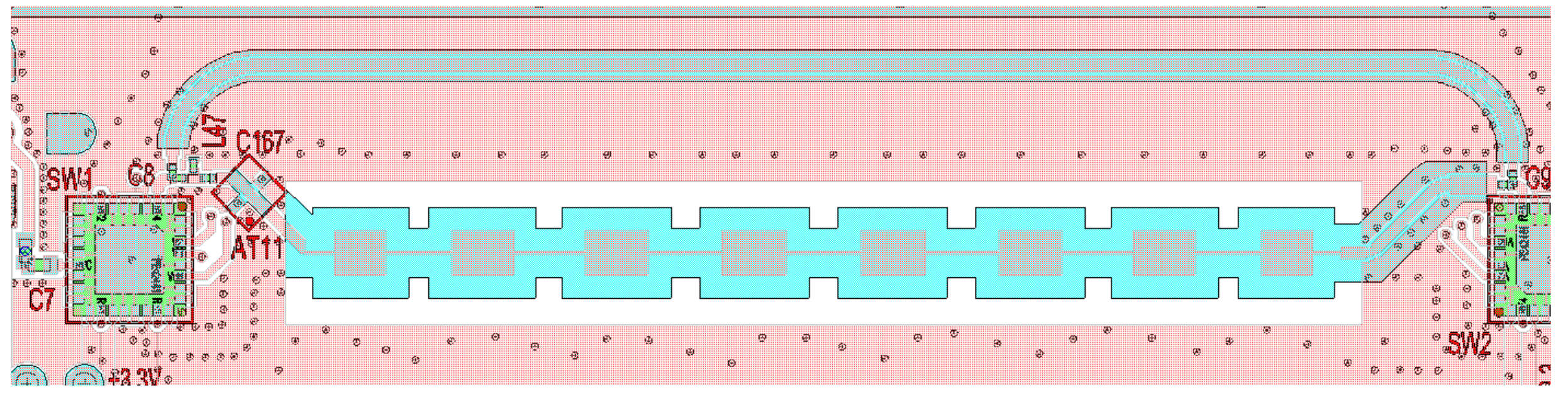
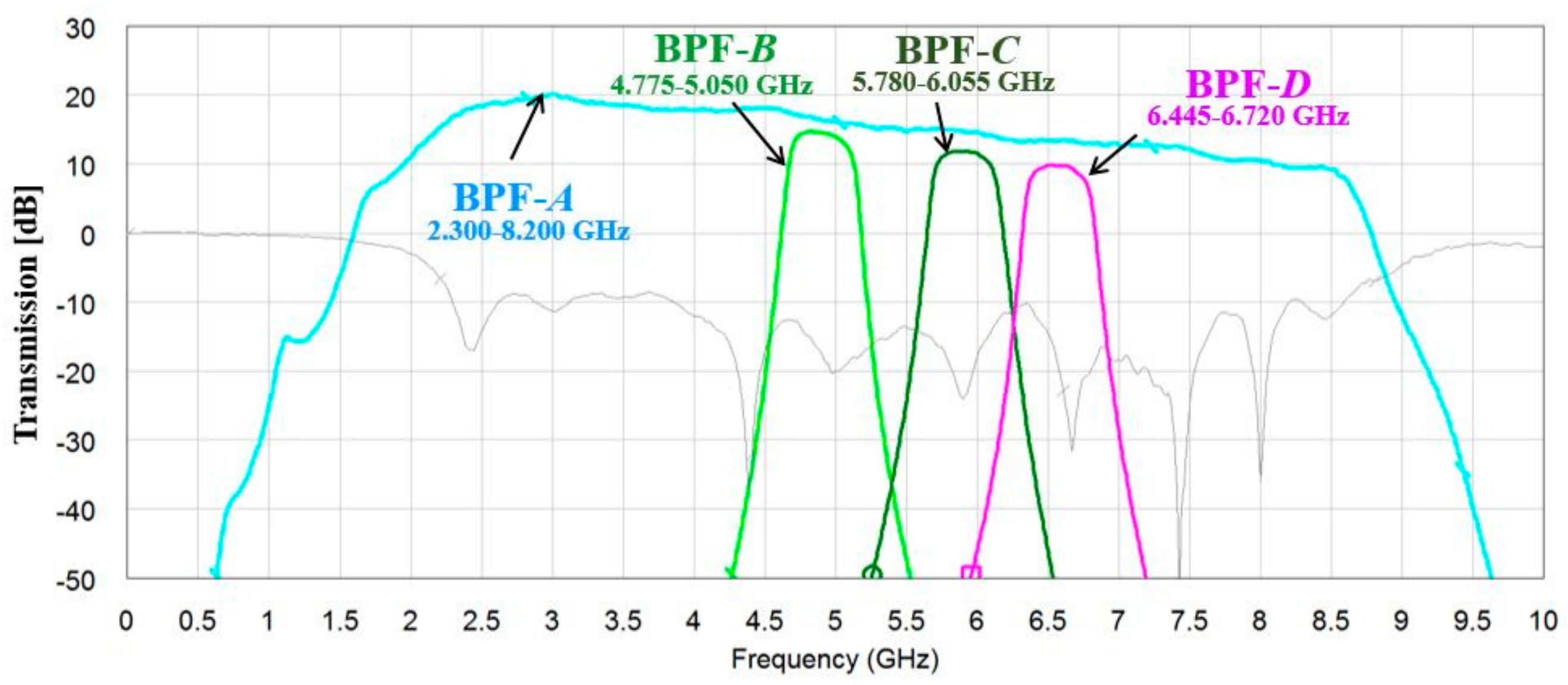
Switched filter banks: band pass filter (BPF) frequency range and LO frequencyBPF-A: 2.300–8.200 GHz; (LO tuning fLO = 2.950–8.575 GHz)
BPF-B: 4.775–5.050 GHz; fLO = 5.425 GHz
BPF-C: 5.780–6.055 GHz; fLO = 6.430 GHz
BPF-D: 6.445–6.720 GHz; fLO = 7.095 GHz
Signal transportationTwo IF output signals transported over a single optical fiber (IFoF) using WDM
Number of wavelength division multiplexing (WDM) fiber-optics link16
Control moduleOptical fiber-Ethernet media-converter and microcontroller for BPF selection and LO power and printed circuit board (PCB) temperature monitoring

