Article

A 30–40 GHz CMOS Receiver Front-End with 5.9 dB NF and 16.5 dB Conversion Gain for Broadband Spectrum Sensing Applications

1
NICE Laboratory, Korea Advanced Institute of Science and Technology (KAIST), Daejeon 341-141, Korea
2
Department of Electronics and Control Engineering, Hanbat National University, Daejeon 305-719, Korea
*
Author to whom correspondence should be addressed.
Electronics 2019, 8(5), 593; https://doi.org/10.3390/electronics8050593
Submission received: 5 April 2019 / Revised: 16 May 2019 / Accepted: 22 May 2019 / Published: 27 May 2019
(This article belongs to the Section Microwave and Wireless Communications)

Abstract

:
A broadband receiver front-end with low noise figure and flat conversion gain response is presented in this paper. The receiver front-end is a part of the broadband spectrum sensing receiver and processes 30–40 GHz of broad input spectrum followed by down-conversion to DC-10 GHz of IF signal. The proposed work is comprised of a low noise amplifier (LNA), on-chip passive Balun, down conversion mixer, and output buffer. To achieve front-end target specification over 10 GHz input bandwidth, the stagger-tuned LNA is employed and the down conversion mixer is loaded with a 3rd-order LC ladder low pass filter. The prototype chip was implemented in 45 nm CMOS technology. The chip achieves 10.3–16.5 dB conversion gain, 5.9 dB integrated NF, and −11 dBm IIP3 from 30 to 40 GHz. The chip is realized within 0.42 mm 2 and consumes 96 mW from a 1.2 V supply.

1. Introduction

Modern wireless transceivers operate in a spectrum-crowded environment due to numerous communication standards introduced to meet the different needs of end-users. The opportunistic utilization of the available spectrum is proposed to maximize the bandwidth usage and achieve a high data rate [1,2]. Then, a broadband receiver solution for spectrum sensing applications is essential to achieve the opportunistic utilization of the valuable resource, also known as cognitive radio. The work in [3] proposed a frequency channelization receiver architecture as one of the attractive solutions to achieve an expeditious spectrum utilization. The channelization receiver system adopts both parallel and series channelization, which help relax the RF front-end requirements and achieve fast frequency spectrum analysis with high dynamic range. The channelization receiver requires a separate RF front-end solution. The broadband input signal branches into parallel RF front-ends with equal bandwidth. The receiver front-end presented in this paper is able to accommodate one of the parallel front-end signal paths, which translates a 30–40 GHz (Ka-band) RF input signal to DC-10 GHz IF signals while maintaining a good signal-to-noise ratio. The critical specification of the proposed receiver front-end is the 10 GHz bandwidth in both the RF and IF frequency range, which is hard to achieve at the same time. Thus, various techniques to improve the operating bandwidth of each block are applied to the proposed receiver design. At the same time, the front-end has to provide low noise and high linearity requirements to have a wide dynamic range [3]. These requirements are satisfied with a newly proposed input matching network utilizing gate to drain feedback capacitance and a linear down-conversion mixer with current-reuse.
The wireless receiver operating at the Ka-band frequency can be utilized in many applications. First of all, to support the high data rate needed in fifth generation (5G) communication, unused millimeter-wave (mm-wave) frequency range including Ka-band has become a very attractive candidate. The 5G transceiver operating at Ka-band was studied in many previous works as a result [4,5,6,7]. Another application of the Ka-band frequency range is ultra wideband (UWB) automotive radar system. To achieve a resolution of a few centimeters, Ka-band is utilized in the receiver front-end of UWB short-range radar applications [8,9]. Satellite communication systems is another example of utilizing the Ka-band frequency range while providing a smaller form-factor at the system level [10,11].
This paper is an extended version of the work presented in [12]. The detailed optimization methods to achieve broadband operation are presented. Unpublished evidence of the validity of the proposed receiver front-end at Ka-band frequency is provided in this work. The low noise amplifier (LNA) input matching condition for stable operation is given. The mixer bandwidth extension due to the peaking inductor is analyzed based on the analog filter theory and compared with one without the peaking inductor
The organization of the paper is as follows. The system architecture is explained in Section 2. Section 3 describes the structure and design considerations of major building blocks to meet the broadband and high performance requirements. Measurement results are presented in Section 4, and concluding remarks are provided in Section 5.

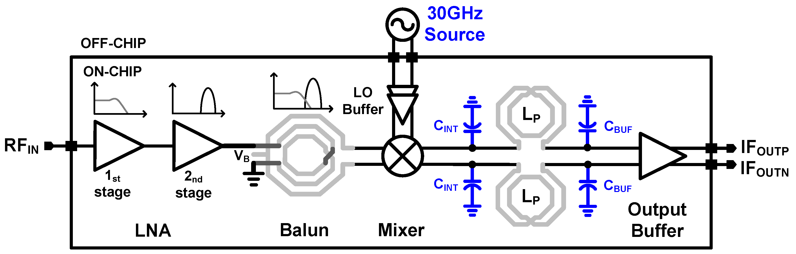
2. Overall RF Front-End System

Figure 1 shows the system architecture of the proposed receiver front-end. The proposed work is targeting a 30–40 GHz frequency range broadband input signal with single-ended configuration. The two-stage stagger-tuned low noise amplifier (LNA) provides signal amplification while providing broadband operation bandwidth. The second stage of LNA is loaded with an on-chip transformer, which performs single-to-differential signal conversion. Balun operation in this work is essential not only for its robustness to common-mode noise and interference but also for its good receiver stability. A 30–40 GHz RF signal is then down-converted to a DC-10 GHz IF frequency band by an active push–pull type mixer loaded by 3rd-order LC ladder filter. An IF signal is delivered to an off-chip 50 Ω load through the common-source configured output buffer.

3. Building Blocks Designs

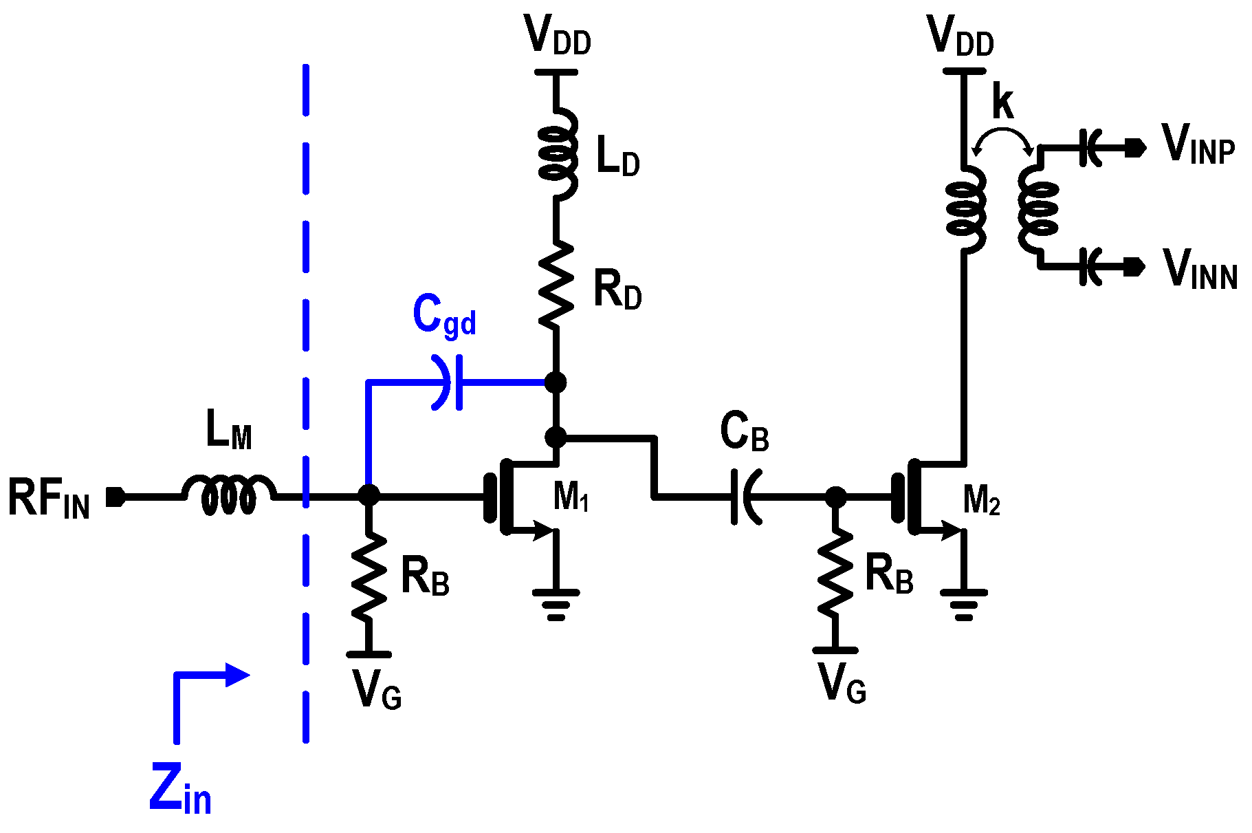
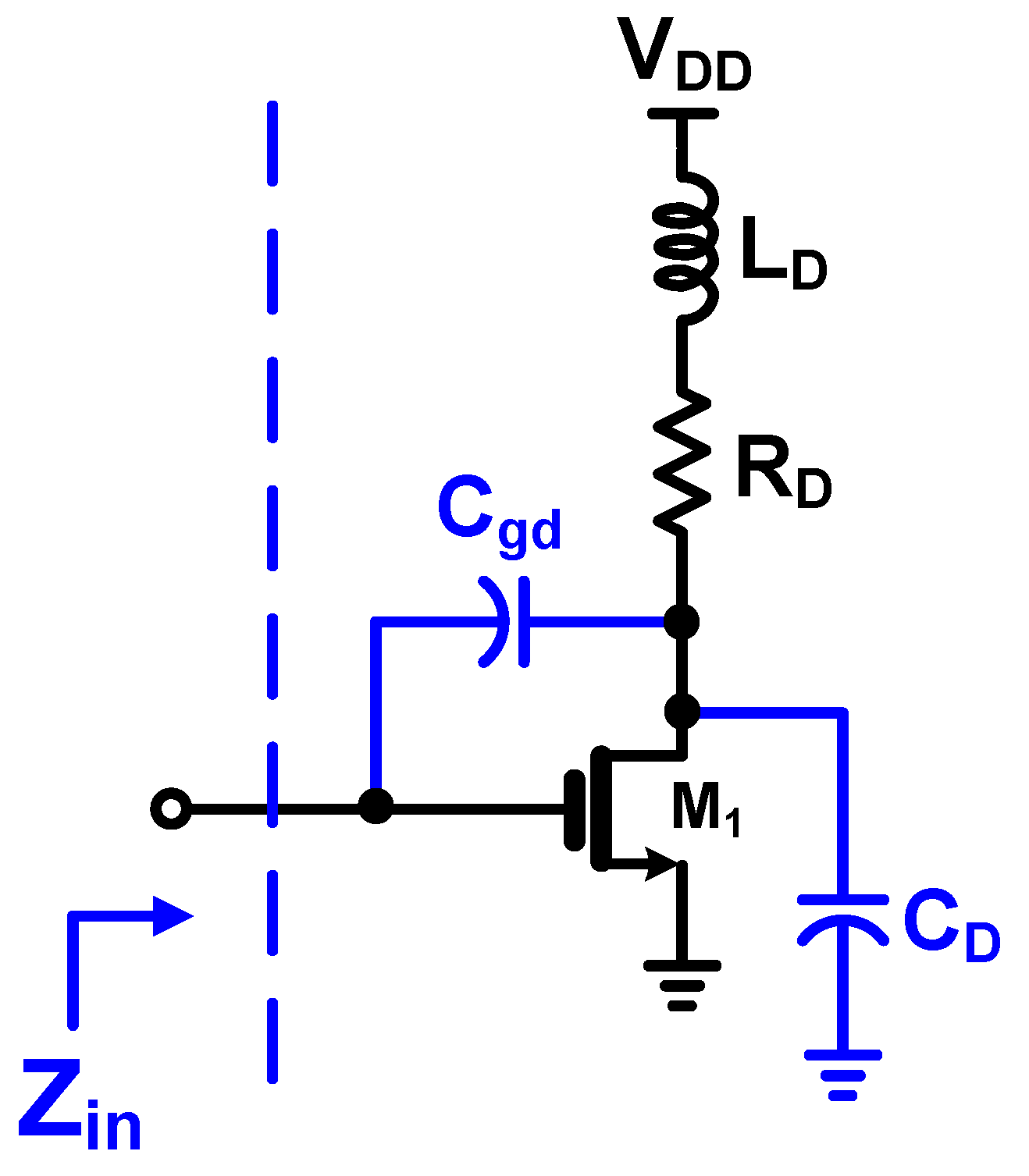
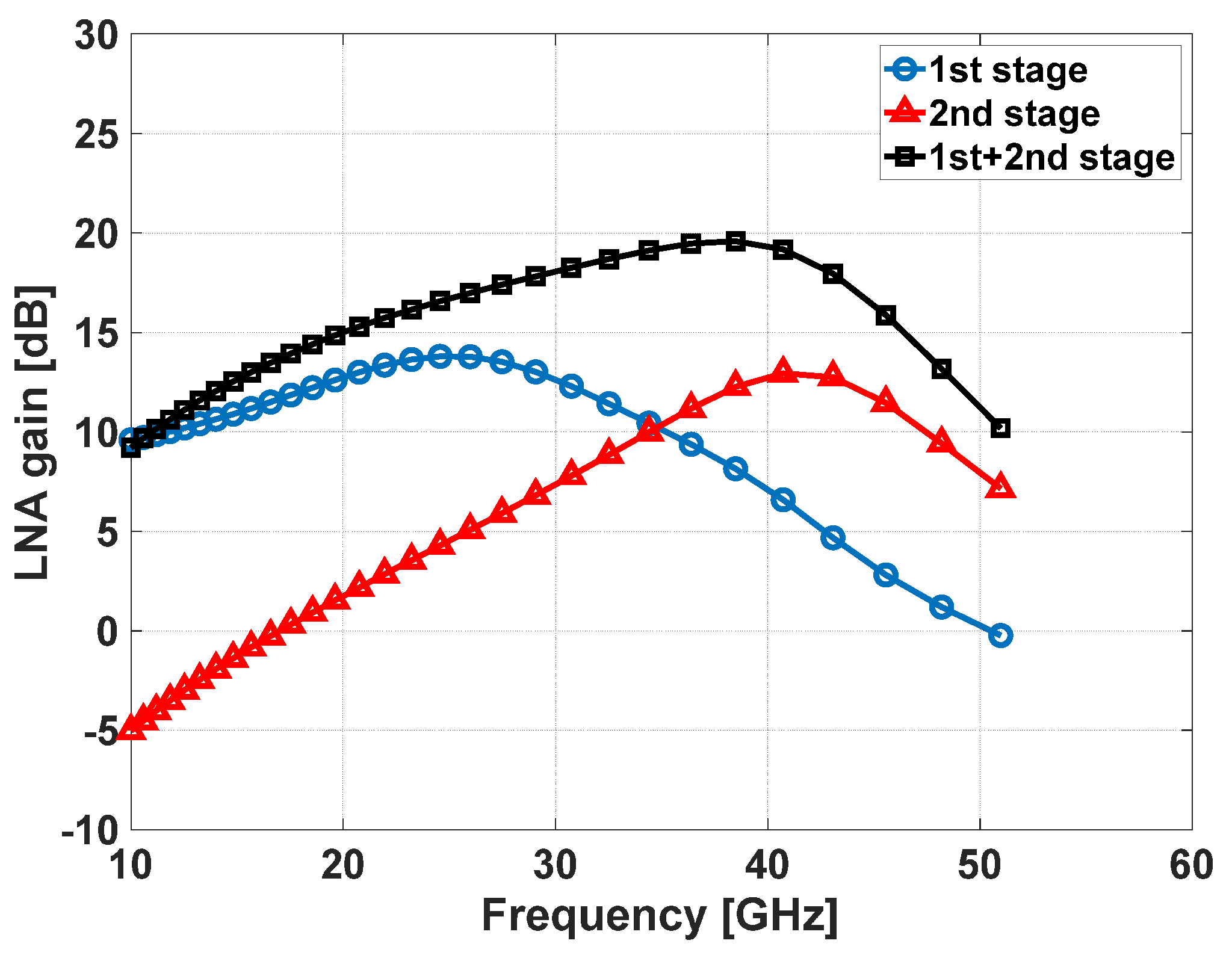
3.1. Low Noise Amplifier (LNA)

Figure 2 shows the schematic of the two-stage LNA for the proposed receiver front-end. The first stage of the LNA is a common-source amplifier stage with inductive peaking load. In contrast to the conventional inductor degenerated LNA [13,14], the common-source amplifier with parasitic coupling capacitance (C g d ) is employed to achieve the input matching without sacrificing noise performance due to a degenerated inductor at the source.
The schema of the LNA’s first stage, calculating the input matching condition, is provided in Figure 3. C D denotes the combination of interconnected line parasitic, ac-coupling and second-stage gate-source capacitances. The real part of input impedance (Re(Z i n )) seen at the gate of trans-conductance (g m ) stage is derived here to show the input matching condition. The effect of C g s is neglected since they merely functions as a shunt components in parallel with the derived Re(Z i n ) expressed as
R e ( Z i n ) = ( C D + C g d ) ( g m 1 L D ω 2 + g m 1 R D 2 + R D ) ( R D C D + g m 1 L D ) A ω ,
where A = ( R D C D + g m 1 L D ) 2 ω 2 + ( g m 1 R D L D C D ω 2 + 1 ) 2 . As shown in Equation (1), with the help of the reactive load of the LNA (L D ,C D ) and C g d , Z i n exhibits the real impedance suitable for input matching. To achieve 50 Ω input matching and avoid potential instability, Re(Z i n ) should have a positive value. A always has a positive sign, so the numerator of Re(Z i n ) determines the stability. The numerator of Re(Z i n ) has a positive value, regardless of frequencies, when D = ( C D + C g d ) ( g m 1 R D 2 + R D ) ( R D C D + g m 1 L D ) is larger than 0. Through some calculations, it can be proven that the proposed LNA exhibits positive real impedance if R D > L D / C D .
Figure 4 shows the stable and unstable region in terms of the value of R D . Table 1 provides the values of real design parameters. To achieve the stable condition, R D should be higher than around 33 Ω . Based on these derivations of Re(Z i n ), R D was selected to 44 Ω in our design. The input inductor, L M , cancels the reactive part of Z i n and thus achieves broadband input matching over 10 GHz of RF bandwidth. The second-stage provides additional gain of LNA with a 2:1 turn ratio passive Balun as a stagger-tuned load [15]. Note that the receiver front-end needs to cover a 30–40 GHz input bandwidth and the first-stage LNA load works as the low-Q band-pass filter centered at 25 GHz. Then, the stagger-tuned load in the second stage helps to compensate the gain at high-frequency regimes with a 40 GHz resonance frequency. The combinational effect due to two-stage stagger-tuned implementation gives the center frequency located at 38 GHz.
The simulation result shows that the entire LNA exhibits a 28–45 GHz wide bandwidth, as depicted in Figure 5.

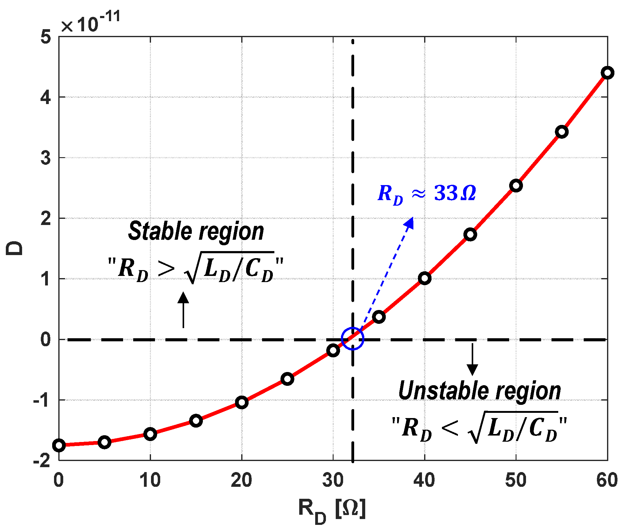
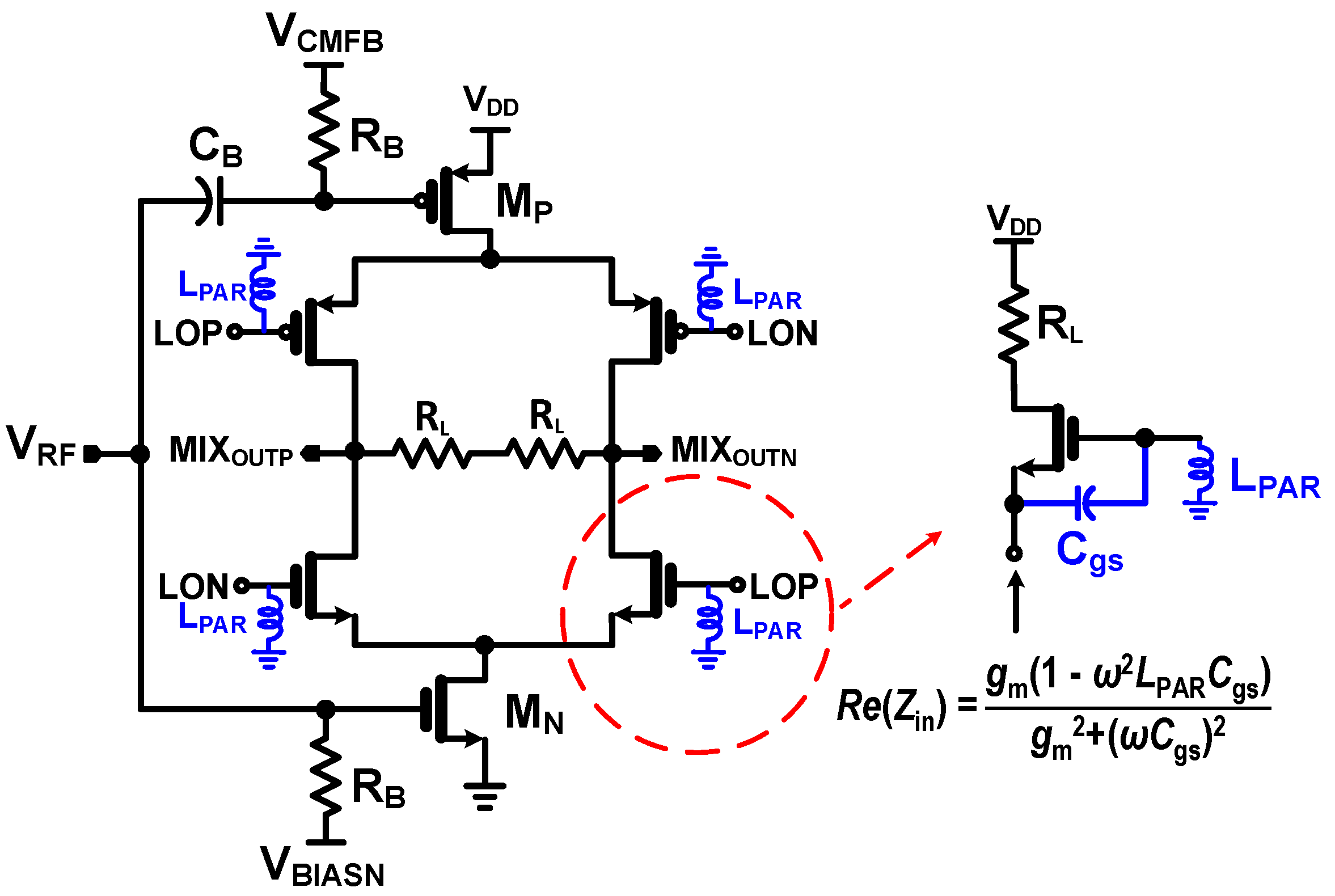
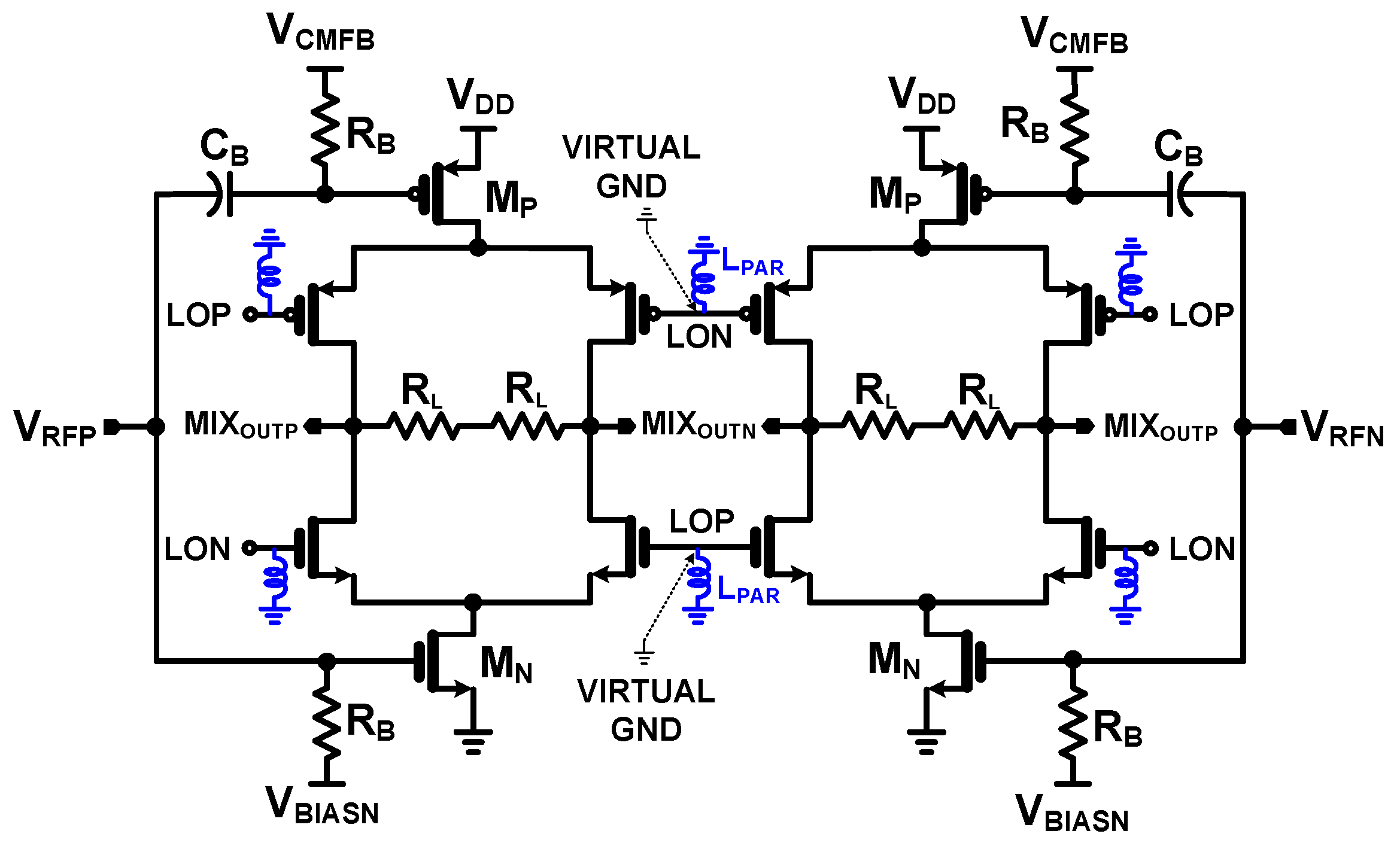
3.2. Down-Conversion Mixer

Figure 6 shows the down-conversion mixer in push–pull configuration. The conversion gain of the mixer can be expressed as A v = 2 π (g m p + g m n )R L , where g m p and g m n denote the trans-conductance due to NMOS and PMOS g m stage of the mixer, and R L is the load impedance. The complementary g m -stage input doubles the conversion gain with the given bias current. It also improves the noise and linearity performances. The mixer in the proposed receiver front-end needs to down-convert a 30–40 GHz input signal to a DC-10 GHz IF signal, which gives a strict trade-off between conversion gain and the bandwidth. We employed the peaking inductor at the load as part of the C-L-C LC ladder filter, whose detailed analysis is given in the next section. The down-conversion mixer interfaced with differential outputs of Balun is the double-balanced structure. We employed the double-balanced structure here even though the push–pull configuration is immune to LO-feedthrough effects [16]. Instead, a double-balanced structure is chosen to avoid parasitic oscillation with the single-balanced mixer configuration.
Figure 7 shows a schema of the single-balanced mixer with parasitic inductance at gate and the capacitance in the switching stages of the mixer due to the parasitic routing effects. As shown in Figure 7 (right), the impedance seen at the source of the switching stage can have a negative real part due to the parasitic inductance at gate and the parasitic capacitance, C g s , of the switching stage. This negative resistance causes the undesired oscillation in the single-balanced mixer. On the other hand, because LOP and LON nodes are virtual grounds in the double-balanced structure (Figure 6), the structure is robust to parasitic oscillation.

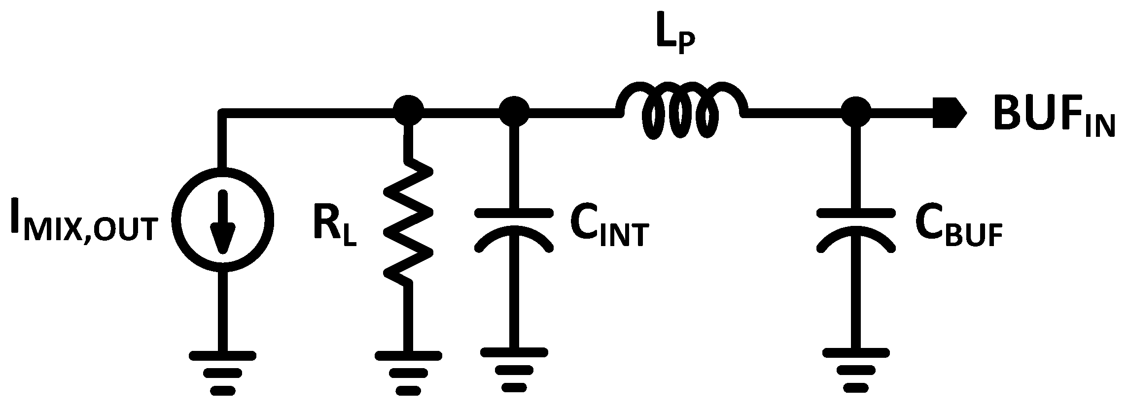
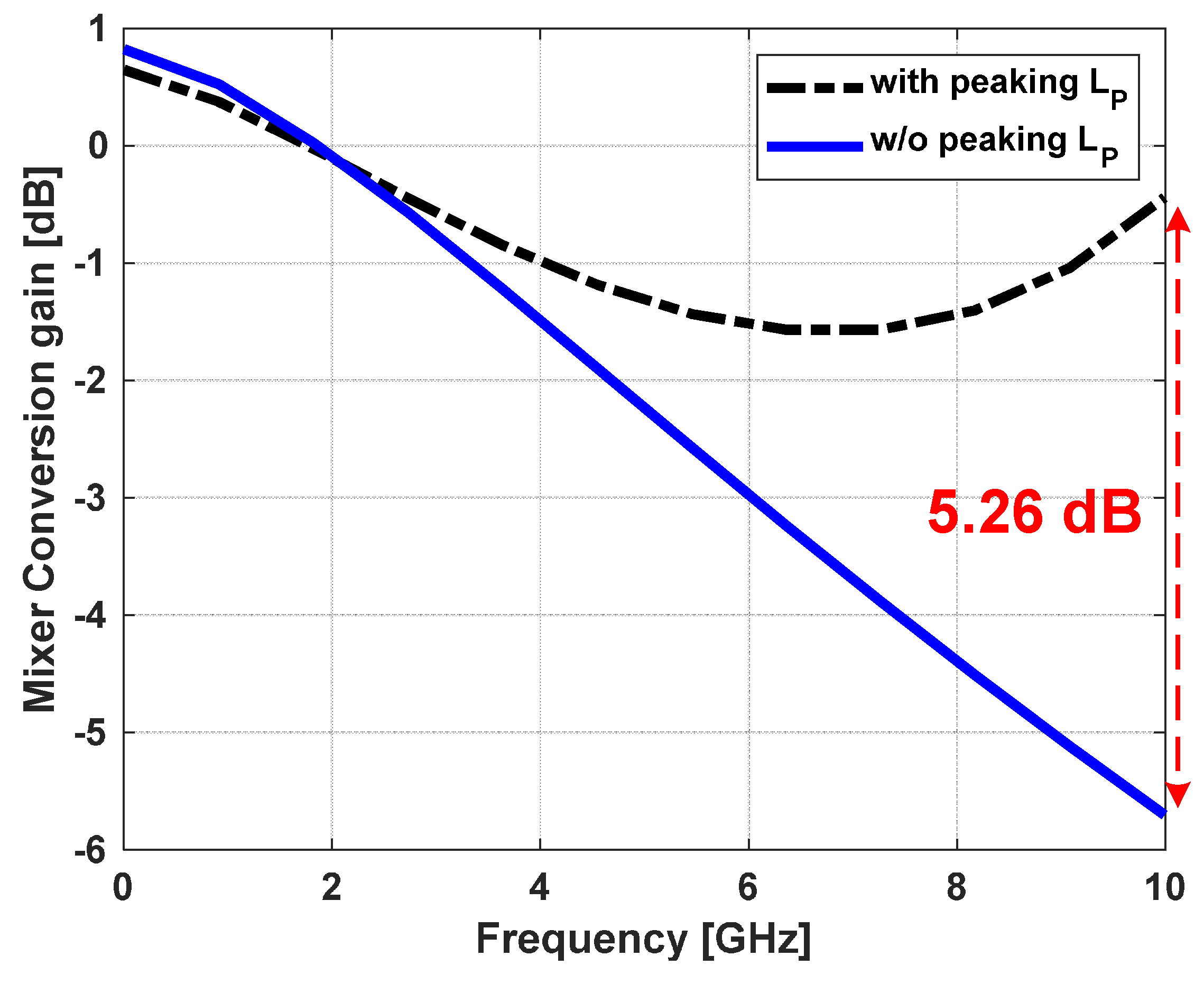
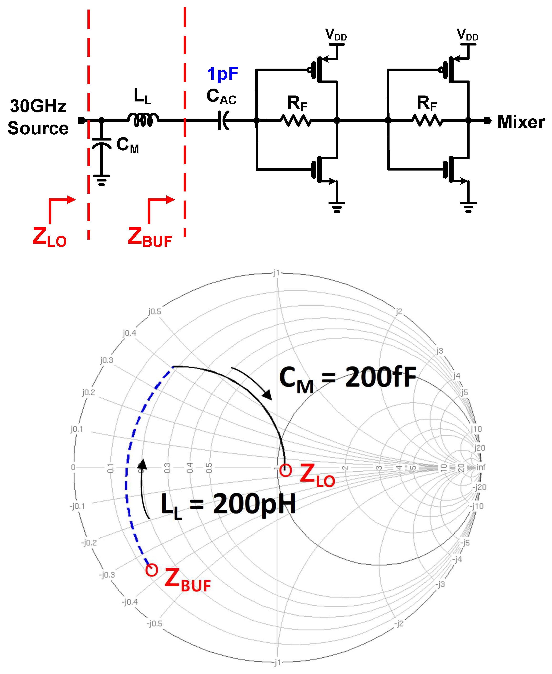
3.3. Third-Order LC Ladder Filter and LO Buffer

In mixer design, the trade-off between conversion gain and bandwidth is significant because the mixer operates in a broad bandwidth. To alleviate the gain drop at high frequency, an additional inductor is put between the mixer load and output buffer. With the introduced peaking inductor (L P ), we can model the interface between the mixer load and the output buffer as a C-L-C ladder filter with single termination at the source. Figure 8 shows the single-ended representation of the interface network. R L is the output resistance of the mixer, C I N T denotes the interconnection lines’ parasitic capacitance parallel with the parasitic capacitance of the mixer switching stage, and C B U F denotes the input capacitance of the output buffer. The transfer functions of conversion gain without and with inductor, L P , are presented as follows
A v ( s ) = 2 / π ( g m p + g m n ) R L 1 + s R L ( C I N T + C B U F ) ,
A v , 3 r d ( s ) = 2 / π ( g m p + g m n ) R L 1 + s R L ( C I N T + C B U F ) + s 2 L P C B U F + S 3 L P C B U F C I N T R L .
By adding L P , the conversion gain has a third-order response, and we synthesized the pole location following the Chebyshev filter realization to maximize the bandwidth [17]. The condition for a third-order Chebyshev filter dictates the following design parameter. The third-order Chebyshev filter with a 2 dB ripple was chosen with normalized pole locations at S 1 , 2 N = −(0.185 ± j0.923) and S 3 N = −0.369. With R L = 86 Ω , C I N T = 136 fF and C B U F = 234 fF for the given bias in the LC ladder network, L P was chosen to the value of 1 nH, which gives the desired filter transfer function.
The effect of the bandwidth extension with third-order LC ladder filter is clearly seen in Figure 9. At the band-edge (10 GHz IF frequency), the conversion gain is improved by 5.26 dB by employing the inductor peaking load as part of the ladder filter. The required LO signal of 30 GHz in the proposed receiver front-end is injected from the off-chip source. To ensure maximum signal reception at such a high frequency, we employed the reactive matching network to match 50 Ω reference impedance. The matching network is implemented with a parallel capacitor and series inductor.
Figure 10 shows the value of the matching components as well as the trajectory from the gate of the LO buffer to the 50 Ω . The series inductor is realized with serpentine line inductance from the pad to the active circuit. This line inductance is clearly noticeable from the chip photograph shown in Figure 11. The LO buffer is realized with two-stage inverter-type amplifiers, where the first stage is AC coupled to the off-chip source, and the second stage is DC coupled to maximize the f t .

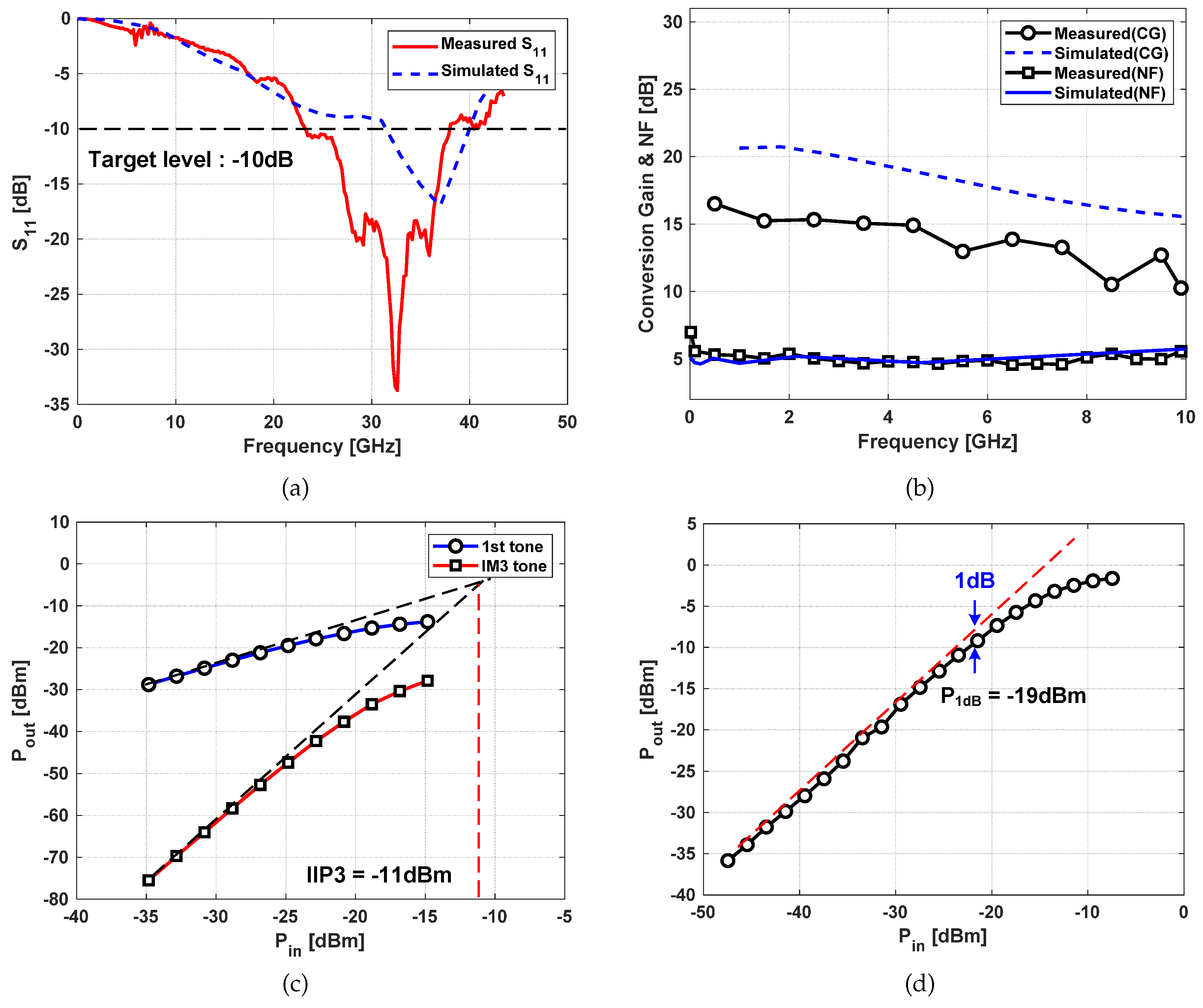
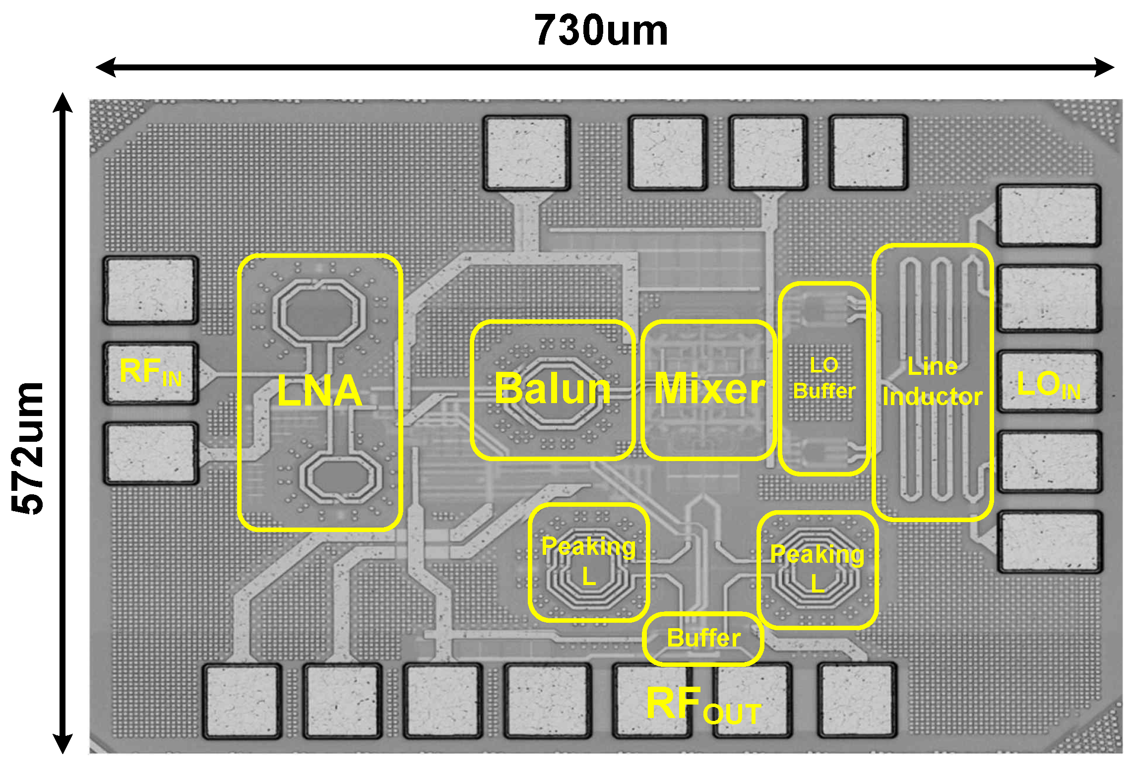
4. Measurement Results

The proposed receiver front-end was designed in TSMC 45 nm CMOS technology. The proposed receiver front-end was simulated with SpectreRF from Cadence and the electromagnetic effects of critical interconnect lines were considered by Advanced Design System (ADS). The fabricated chip was encapsulated in a quad flat no leads (QFN) package for connecting dc pads and IF output. The RF and LO signals were applied using on-wafer probing to reduce the losses and mismatches. Keysight N5234A as used for S-parameter measurement and Keysight N9010A-544 was used for spectrum analysis and noise figure measurement. The chip photograph of the implemented receiver front-end is shown in Figure 11. The total area of the chip is 0.42 mm 2 , and the core circuits occupies 0.21 mm 2 . The entire circuit consumes 96 mW with 1.2 V power supply. Figure 12a shows the input reflection coefficient (S 11 ). The target level was chosen as −10 dB for stable power transfer. There was a little frequency shift in S 11 due to the un-accounted parasitics in the interconnect line, but the broad impedance matching performance with S 11 <−9 dB was achieved within the 30–40 GHz frequency range. Figure 12b shows the conversion gain and double-sideband NF over the 10 GHz IF frequency range of the implemented receiver front-end. The measured conversion gain was 10.3–16.5 dB. We measured a maximum conversion gain of 16.5 dB at 50 MHz IF frequency. Measured NF integrated over a 10 GHz IF bandwidth was 5.9 dB, whereas the simulated NF over the same integration bandwidth was 5 dB. Linearity performance is shown in Figure 12c. The measured IIP3 was around −11 dBm, based on the two tone input injection tones at 35 GHz and 35.1 GHz. A large signal linearity performance was measured with a 1 dB compression point as shown in Figure 12d. The implemented receiver front-end showed −19 dBm of 1 dB compression point (P1dB). Measured P1dB and IIP3 showed an 8 dB difference, close to the theoretical discrepancy between the two [18]. Table 2 summarizes the performances and compares the performances with other recent works. It is clear that the proposed front-end exhibits the largest RF and IF bandwidth while having a small die area, moderate power consumption, and comparable performance to previous studies. Therefore, it is proven that the proposed front-end is suitable for the various Ka-band applications as well as channelization receiver systems.

5. Conclusions

The 30–40 GHz receiver front-end for broadband sensing receivers is implemented. The two-stage stagger-tuned LNA and push–pull type mixer loaded with third-order LC ladder filter are employed to achieve the broadband operation with low current consumption. To ensure unconditional stability of the receiver front-end with single-ended input signal, a double-balanced mixer operation is employed with on-chip Balun. This chip achieves a maximum conversion gain of 16.5 dB, 5.9 dB integrated NF, and −11 dBm IIP3 from 30 GHz to 40 GHz. The power consumption is 96 mW from a 1.2 V supply. The active area is only 0.21 mm 2 . The proposed receiver front-end shows the widest RF and IF operating bandwidth with good performance and moderate power consumption compared to previous works.

Author Contributions

Conceptualization, D.R.U. and J.K.; methodology, D.R.U.; validation, H.J. and S.S.; formal analysis, H.J. and D.R.U.; investigation, H.J.; resources, J.K.; data curation, H.J. and D.R.U.; writing–original draft preparation, H.J.; writing–review and editing, J.K., D.R.U., S.S., and J.K.; visualization, H.J.; supervision, S.K.-H. and S.-G.L.; project administration, S.-K.H.; funding acquisition, S.-G.L.

Funding

This work was funded by the Civil-Military Technology Cooperation Program through the Defense Acquisition Program Administration and the Ministry of Trade, Industry, and Energy, South Korea.

Conflicts of Interest

The authors declare no conflict of interest.

References

  1. Haykin, S. Cognitive radio, brain-empowered wireless communications. IEEE J. Sel. Areas Commun. 2005, 23, 201–220. [Google Scholar] [CrossRef]
  2. Joseph, M.; Gerald, Q.M. Cognitive radio: Making software radios more personal. IEEE Pers. Commun. 1999, 6, 13–18. [Google Scholar]
  3. Kim, J.; Utomo, D.R.; Dissanayake, A.; Han, S.K.; Lee, S.G. The Evolution of channelization receiver architecture: Principles and design challenges. IEEE Access. 2017, 5, 25385–25395. [Google Scholar] [CrossRef]
  4. Min, B.-W.; Rebeiz, G.M. Single-ended and differential Ka-band BiCMOS phased array front-ends. IEEE J. Solid-State Circuits 2008, 43, 2239–2250. [Google Scholar] [CrossRef]
  5. El-Nozahi, M.; Amer, A.; Sanchez-Sinencio, E.; Entesari, K. A Millimeter-Wave (24/31-GHz) Dual-Band Switchable Harmonic Receiver in 0.18-μm SiGe Process. IEEE Trans. Microw. Theory Tech. 2010, 58, 2717–2730. [Google Scholar] [CrossRef]
  6. Kodak, U.; Rebeiz, G.M. A 42 mW 26–28 GHz phased-array receive channel with 12 dB gain, 4 dB NF and 0 dBm IIP3 in 45 nm CMOS SOI. In Proceedings of the 2016 IEEE Radio Frequency Integrated Circuits Symposium (RFIC), San Francisco, CA, USA, 22–24 May 2016. [Google Scholar]
  7. Yeh, Y.S.; Walker, B.; Balboni, E.; Floyd, B. A 28-GHz Phased-Array Receiver Front End With Dual-Vector Distributed Beamforming. IEEE J. Solid-State Circuits 2017, 52, 1230–1244. [Google Scholar] [CrossRef]
  8. Jain, V.; Sundararaman, S.; Heydari, P. A 22–29-GHz UWB pulse radar receiver fornt-end in 0.18-μm CMOS. IEEE Trans. Microw. Theory Tech. 2009, 57, 1903–1914. [Google Scholar] [CrossRef]
  9. Lin, Y.S.; Lee, J.H.; Huang, S.L.; Wang, C.H.; Wang, C.C.; Lu, S.S. Design and Analysis of a 21–29-GHz Ultra- Wideband Receiver Front-End in 0.18 μm CMOS Technology. IEEE Trans. Microw. Theory Tech. 2012, 60, 2590–2604. [Google Scholar] [CrossRef]
  10. Deng, Z.; Chen, J.; Tsai, J.; Niknejad, A. A CMOS Ku-band single conversion low-noise block front-end for satellite receivers. In Proceedings of the 2009 IEEE Radio Frequency Integrated Circuits Symposium, Boston, MA, USA, 7–9 June 2009. [Google Scholar]
  11. Jong, G.d.; Leenaerts, D.; van der Heijden, E. A fully integrated Ka-Band VSAT Down-Converter. IEEE J. Solid-State Circuits 2013, 48, 1651–1658. [Google Scholar] [CrossRef]
  12. Jung, H.; Utomo, D.R.; Shin, S.; Han, S.K.; Lee, S.G.; Kim, J. Ka-band RF Front-End with 5 dB NF and 16 dB conversion gain in 45 nm CMOS technology. In Proceedings of the IEEE International SoC Design Conference, Daegu, Korea, 12–15 November 2018. [Google Scholar]
  13. Shaeffer, D.K.; Lee, T.H. A 1.5-V, 1.5-GHz CMOS low noise amplifier. IEEE J. Solid-State Circuits 1997, 32, 745–759. [Google Scholar] [CrossRef]
  14. Nguyen, T.K.; Kim, C.H.; Ihm, G.J.; Yang, M.S.; Lee, S.G. CMOS low-noise amplifier design optimization techniques. IEEE Trans. Microw. Theory Tech. 2004, 52, 1433–1442. [Google Scholar] [CrossRef]
  15. Wu, C.C.; Chou, M.F.; Wuen, W.S.; Wen, K.A. A low power CMOS low noise amplifier for ultra-wideband wireless applications. In Proceedings of the IEEE International Symposium on Circuits and Systems (ISCAS), Kobe, Japan, 23–26 May 2005. [Google Scholar]
  16. Liu, Y.H.; Huang, X.; Vidojkovic, M.; Ba, A.; Harpe, P.; Dolmans, G.; de Groot, H. A 1.9 nJ/b 2.4 GHz multistandard (Bluetooth Low Energy/Zigbee/IEEE802. 15.6) transceiver for personal/body-area networks. In Proceedings of the IEEE International Solid-State Circuits Conference (ISSCC), San Francisco, CA, USA, 17–21 February 2013. [Google Scholar]
  17. Van Valkenburg, M.E. Analog Filter Design, 2nd ed.; Holt, Rinehart, and Winston: New York, NY, USA, 1982. [Google Scholar]
  18. Behzad, R. RF Microelectronics, 2nd ed.; Prentice Hall: Upper Saddle River, NJ, USA, 1998; ISBN 978-0-13-713473-1. [Google Scholar]
  19. Li, C.H.; Kuo, C.N.; Kuo, M.C. A 1.2-V 5.2-mW 20–30-GHz Wideband Receiver Front-End in 0.18-μm CMOS. IEEE Trans. Microw. Theory Tech. 2012, 60, 3502–3512. [Google Scholar]
  20. Wang, P.Y.; Shen, Y.C.; Chou, M.C.; Wu, T.L.; Chang, Y.C.; Chang, D.C.; Hsu, S.S.H. A BiCMOS Monolithic Ka-Band Down-Converter for Satellite Communication Systems. In Proceedings of the IEEE MTT-S International Microwave Symposium (IMS), Phoenix, AZ, USA, 17–22 May 2015. [Google Scholar]
  21. Ding, B.; Yuan, S.; Zhao, C.; Tao, L.; Tian, T. A Ka band FMCW Transceiver front-end with 2GHz bandwidth in 65-nm CMOS. IEEE Trans. Circuits Syst. II Express Briefs 2019, 66, 212–216. [Google Scholar] [CrossRef]
Figure 1. Receiver front-end architecture: stagger-tuned two-stage low noise amplifier (LNA), down-conversion mixer loaded with 3-stage LC ladder filter, LO buffer, and output buffer.
Electronics 08 00593 g001
Figure 2. Schema of the LNA.
Electronics 08 00593 g002
Figure 3. Schema of the LNA’s first stage.
Electronics 08 00593 g003
Figure 4. The condition of R D for LNA input matching and stability.
Electronics 08 00593 g004
Figure 5. The simulated frequency response of the LNA with stagger tuning.
Electronics 08 00593 g005
Figure 6. Schema of the double-balanced mixer.
Electronics 08 00593 g006
Figure 7. Schema of single-balanced mixer.
Electronics 08 00593 g007
Figure 8. Modeling of the mixer load with additional inductor for bandwidth extension.
Electronics 08 00593 g008
Figure 9. Simulated conversion gain of the down-conversion mixer with and without series peaking inductor L P .
Electronics 08 00593 g009
Figure 10. Schema of the two-stage LO buffer with reactive matching and a Smith chart with the trajectory from Z B U F to the 50 Ω .
Electronics 08 00593 g010
Figure 11. Chip photograph of the proposed receiver front-end.
Electronics 08 00593 g011
Figure 12. Measured (a) input reflection coefficient (S 11 ), (b) conversion gain and NF over a 10 GHz IF frequency range; (c) IIP3 with frf1 = 35 GHz and frf2 = 35.1 GHz; and (d) 1 dB compression point with frf = 35 GHz.
Electronics 08 00593 g012
Table 1. LNA design parameters.
ParameterValueDescription
g m 1 76.2 mStransconductance of M 1
L D 230 pHload inductor
R D 44 Ω load resistor
C g d 20 fFparasitic capacitance between gate and drain
C D 200 fFparasitic gate capacitance of M 2
Table 2. Performance comparison.
SpecificationThis WorkTMTT 12 [19]IMS 15 [20]JSSC 17 [7]TICAS-II 19 [21]
RF Frequency [GHz]30–4020–3018.2–21.428–3233.6–36.3
IF Bandwidth [GHz]100.31.3542.3
Gain m a x [dB]16.518.74910.530.9
NF [dB]5.9 1 7.1–14.25.25–6.255.6–8.65.9–7.5
IIP3 [dBm]−11>−7.6>−33.5 2 >−10.6N/A
P 1 dB [dBm]−19>−17.9>−43.3 3 >−16.8−23
P c o n s u m p t i o n [mW]965.280136.5135/27.6 4
TechnologyCMOS 45 nmCMOS 180 nmSiGe 180 nmSiGe 130 nmCMOS 65 nm
Area [mm 2 ]0.42/0.21 5 0.180.4/0.24 5 1.082.16 6
1 Integrated NF (DC-10 GHz), 2 Calculated from OIP3, 3 Calculated from OP 1 dB , 4 Receiver only, 5 Active area, 6 Including transmitter.

