Article

Effect of lateral Gate Design on the Performance of Junctionless Lateral Gate Transistors

1
Department of Physics, Isfahan University of Technology, Isfahan 84156–83111, Iran
2
Faculty of Engineering, Multimedia University, Cyberjaya 63100, Malaysia
3
Center for Quantum Devices, Department of Electrical Engineering and Computer Science, Northwestern University, Evanston, IL 60208, USA
4
Nour, LLC, Wilmette, IL 60091, USA
5
Faculty of Engineering and Built Environment, Universiti Kebangsaan Malaysia (UKM), Bangi 43600, Selangor, Malaysia
*
Author to whom correspondence should be addressed.
Electronics 2019, 8(5), 538; https://doi.org/10.3390/electronics8050538
Submission received: 12 March 2019 / Revised: 2 April 2019 / Accepted: 2 April 2019 / Published: 13 May 2019
(This article belongs to the Section Semiconductor Devices)

Abstract

:
In this paper, we investigate the effect of lateral gate design on performance of a p-type double lateral gate junctionless transistors (DGJLTs) with an air gate gap. The impact of lateral gate length, which modifies the real channel length of the device and gate gap variation down to 50 nm which have been found to be the most influential factors in the performance of the device have been comprehensively investigated. The characteristics are demonstrated and compared with a nominal DGJLTs through three-dimensional technology computer-aided design (TCAD) simulation. At constant channel geometry (thickness and width), when the lateral gate length decreases, the results show constant flatband drain current characteristics while the OFF state current (IOFF) increases significantly. On the other hand, by decreasing the air gap the subthreshold current considerably decreases while the flatband current is constant. Moreover, at a certain gate gap, the gates lose control over the channel and the device simply works as a resistor. Electric field component, carriers’ density, band edge energies, and recombination rate of the carriers inside the channel in depletion and accumulation regimes are analysed to interpret the variation of output characteristics.

1. Introduction

Junctionless transistors (JLTs) have been proposed to improve the electrical performance of conventional field effect transistors (FET) devices [1,2]. In JLTs, the source-channel-drain doping profile is similar. Therefore, the device can be considered as a resistor with two terminals in which a third terminal (gate) modifies the current flows through the channel section. In addition to a simpler structure and fabrication process, other advantages of JLTs such as high ON/OFF current ratio, lower leakage current, lesser sub-threshold slope, low frequency noise and variability were reported in the literature [3,4,5,6,7]. The first junctionless proposed was principally n-type highly doped gated resistor device [8]. Single n-Channel Junctionless Nanowire Transistors and n-Type Poly-Si Junctionless Nanowire Transistor are also amongst the ON channel n-type junctionless devices which have been recently introduced [9,10]. The junctionless transistors were principally turned off based on the depletion of the channel by electric field induced by the gate which mainly can be achieved with shrinking the channel size.
Recently, various material such as InAs [11], Ge/Si core/shell nanowire [12], monolayer MoS2 [13], Transition-Metal-Dichalcogenide [14], MOS-like junctionless Carbon nanotube field effect transistor (MOS-like J-CNTFET) [15], and oxygen-doped TiN ultrathin-body channels [16] have been used as the active channel material of the transistor. Moreover, JLTs have been used in innovative applications for bio-sensing [17,18], transient or biodegradable electronics [19], resonators [20], logic circuits [21] and photodetectors [22]. From the speed and power aspect, reducing gate capacitance of conventional MOS-based devices can be considered as a good option to improve the performance of these devices. A number of studies were performed to address suppression of the gate capacitance [23,24,25,26]. One of the practical options is to find low-κ materials [27,28]. However, the porous structure of low-k materials and the poor structural stability associated with that brings about a reliability problem. As an attractive alternative air gap structure of transistor which takes the advantage of conventional material and vacuum is proposed [29,30,31]. The structure overcomes delay, and power consumption issue associated with conventional devices [25]. Moreover, as it is presented in [32,33] the air gap-based devices may offer better long-term device stability because of lower interface state density, higher breakdown electric fields due to implanting of an airgap, rather than a dielectric, lower gate dielectric constant and hence, lower dielectric capacitance and better hot carrier reliability because there are no bulk oxide traps. The double lateral gate junctionless transistors (DGJLTs), combines the advantage of JLTs and air gap devices all together. The fabrication of DGJLTs through scanning probe lithography (SPL) has been reported in [34,35,36]. Moreover, the operation mechanism and channel geometrical effect (source/drain extensions, channel thickness and width) on the performance of device have also been investigated [37,38,39,40]. The main focus of the present work is devoted towards the impact of lateral gates engineering and particularly lateral gate length (LG) and air gap between the lateral gates and channel on output characteristics of DGJLTs. The variation of output characteristics interpreted based on the variation of electric field components, carriers density inside the channel, band edge energies, and recombination-generation of the carriers. The main analysis of the device was performed between flat band and fully depleted regimes of devices. However, whenever was necessary, the accumulation region also was considered.

2. Device Structure and Simulation Methodology

Figure 1a,b show an isotropic view and a top view of a nominal p-type DGJLT. The device has a silicon thickness and width of 100 nm, and source/drain (S/D) extensions of (Lext = 2 μm), with 1015(cm−3) doping concentration in all active regions of the device, analogues to the DGJLT device proposed and fabricated in [35,38].
The gate length (LG) and gate gap are two parameters of interest in this study (the range of variation is provided in Table 1). Two main sources of the parasitic S/D series resistance RS/RD are the contact resistance (Rcon) and extension resistance (Rext). In this study, for both cases where the LG and gate gap are varied, Rext and Rcon are considered constant; thus, it is possible to purely capture the effect of the desired parameter on output characteristics of the device.
The output electrical characteristics were simulated via 3-D TCAD simulation, using Sentaurus software D-2010.03 tool [41]. The simulation involves a hydrodynamic model along with Shockley–Read–Hall (SRH) and doping-dependent Masetti mobility. The considered mobility model examines the high electric field effect through incorporating the high-field saturation Canali model. According to the geometrical dimensions of the device, the inclusion of quantum effect in the simulators was not essential.

3. Results

3.1. Principle of Operation

The p-type DGJLT device is a normally an ON device, where theON-state is characterized by a conducting channel in the entire silicon body when the applied gate voltage is zero. By applying a positive bias to the lateral gates, the channel cross section can be modulated by depletion of carriers through two lateral air gaps and eventually pushing the conduction path into the pinch-off state (OFF-state). The specific design of the device, with two independent lateral gates which are coupled to the channel through the two air gap capacitors, induces the channel depletion starting from the bottom corner of the channel, from the sides facing the gates, and spread to the centre and the top of the channel [38]. In the linear region and in depletion mode, the drain current ID of the device can be approximated as [20]:
I D = q μ N A t S i [ W 2 W D e p ] L G V D
where μ is carrier mobility, NA is channel doping concentration, WDep is depletion depth, tSi and W are the channel thickness and lateral width of the channel, respectively, and LG is the gate length.

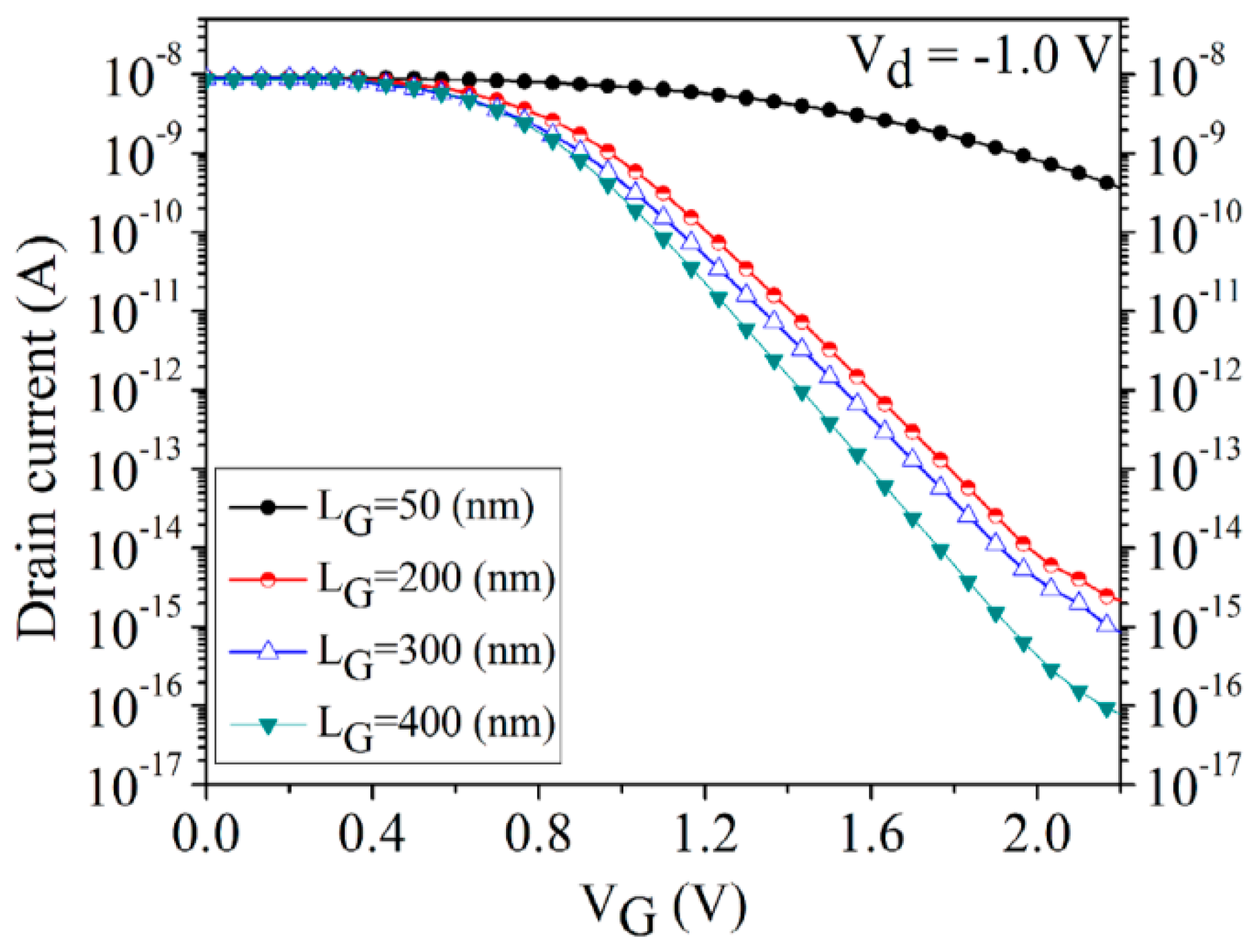
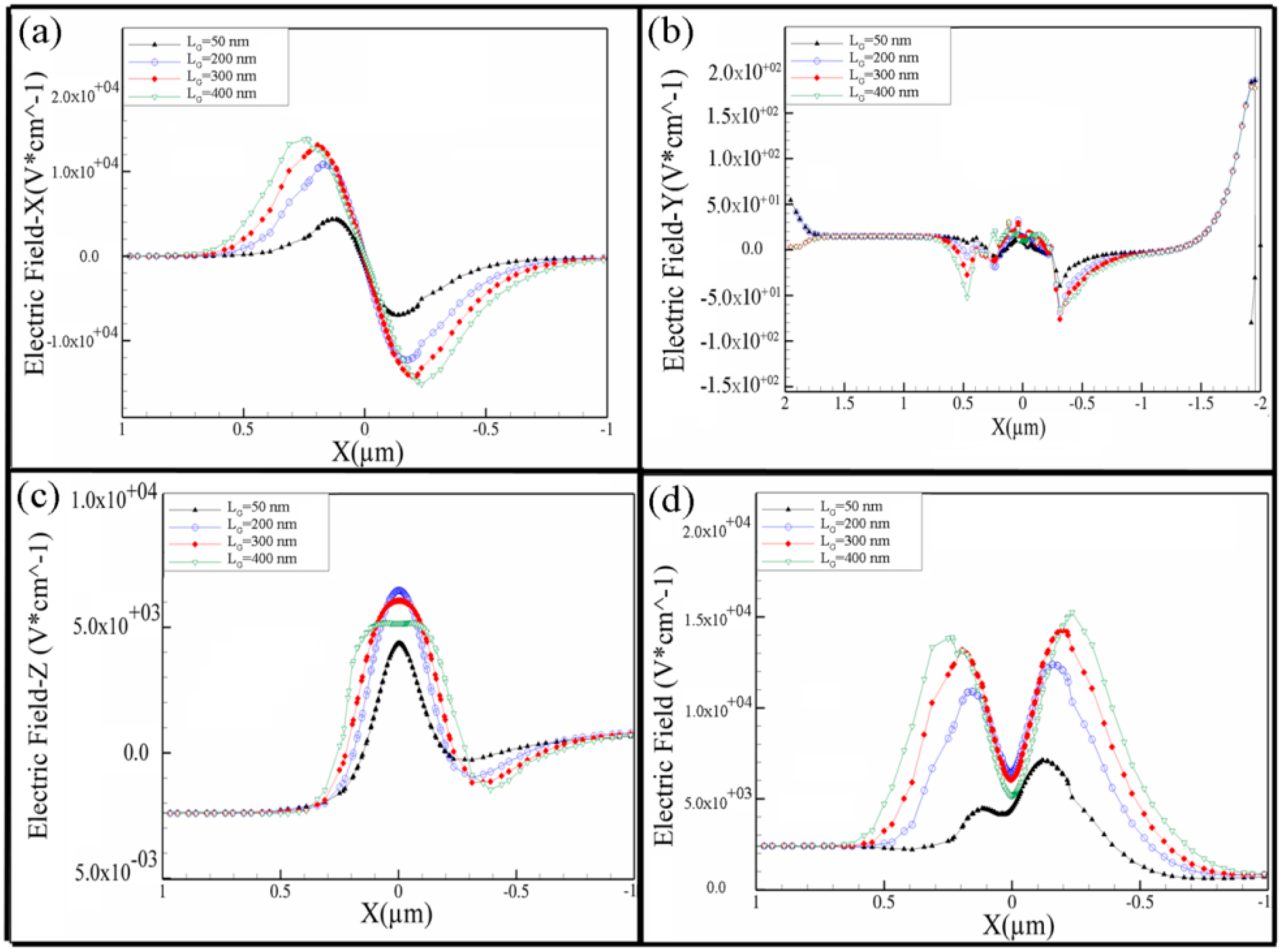
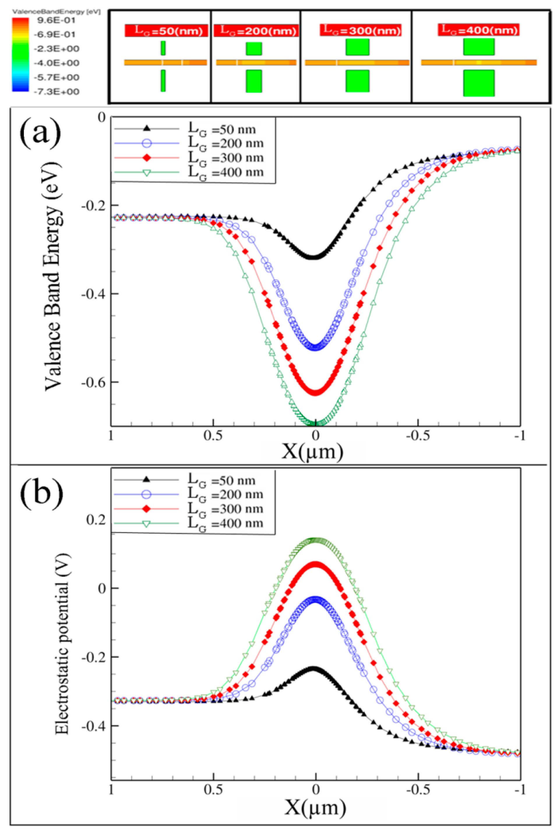
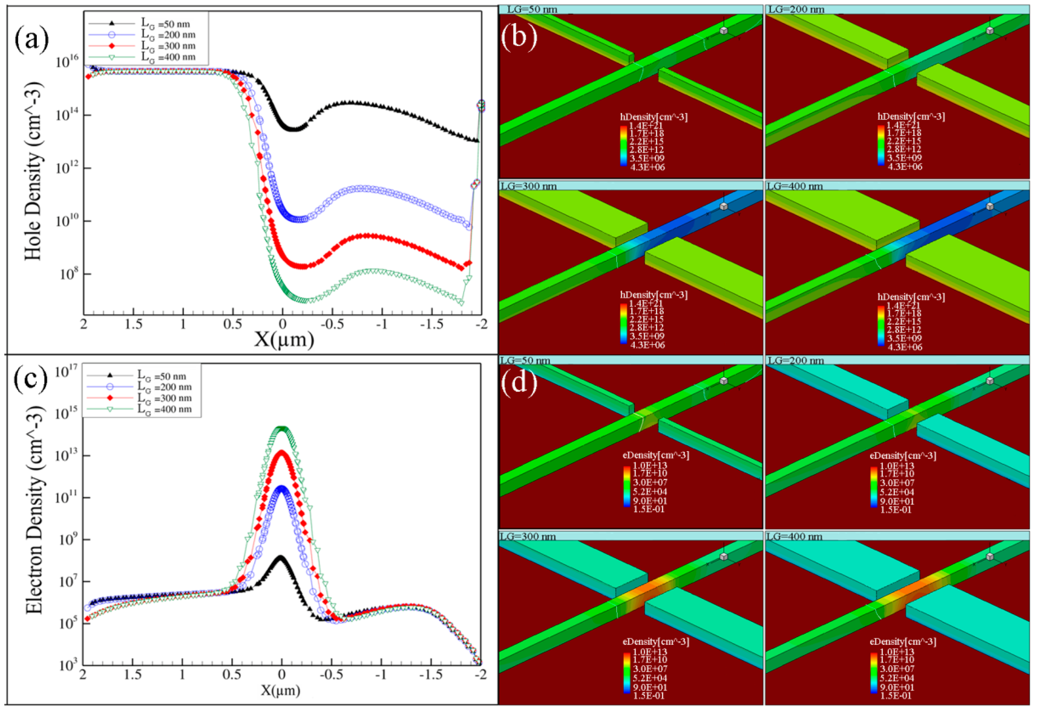
3.2. Effect of Lateral Gate Length (LG) Variation

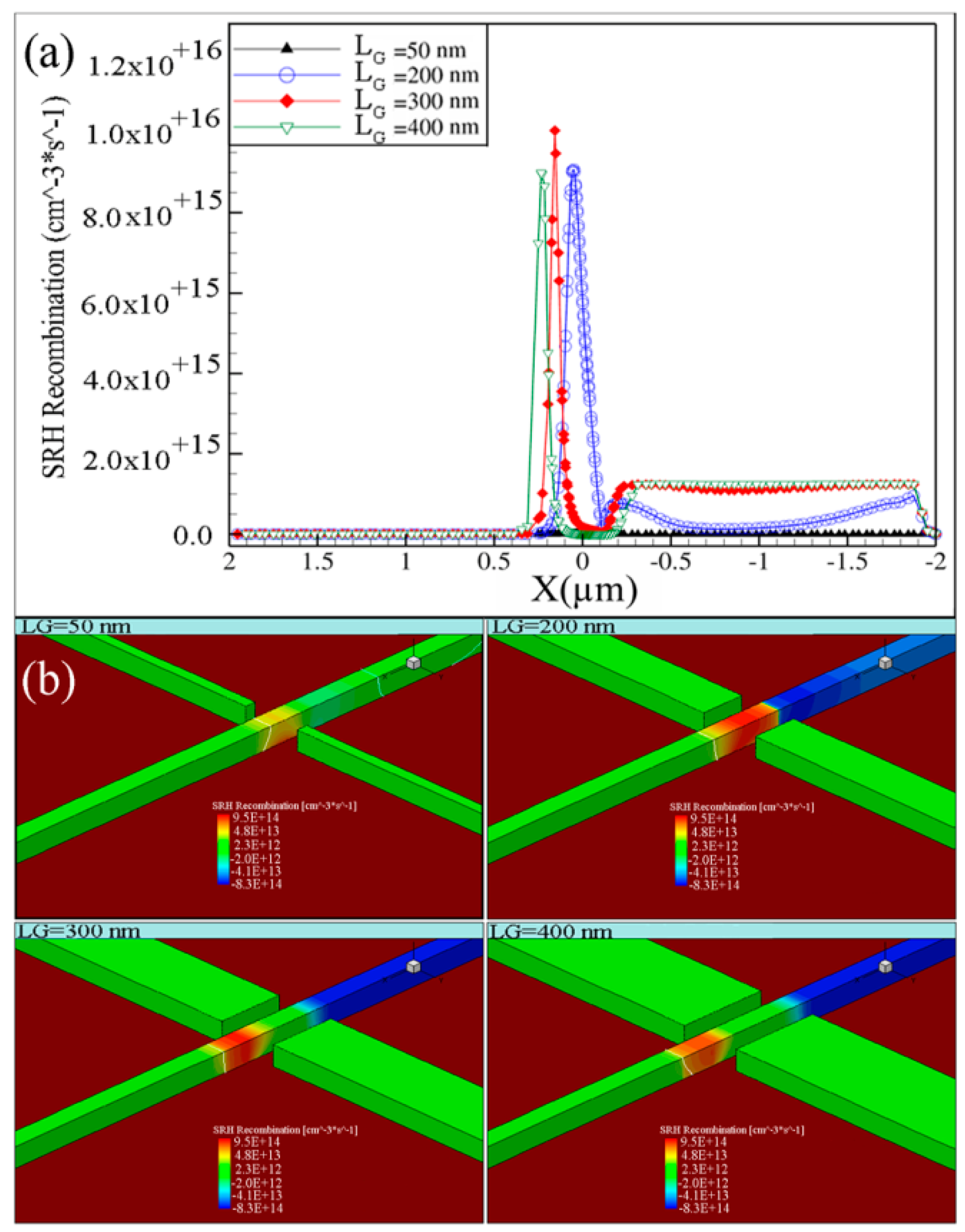
3.2.1. Depletion Regime

The characteristics of the DGJLTs with different lateral LG down to 50 nm are investigated and compared with a nominal device (LG = 200) similar to the fabricated device reported in [35,38]. Figure 2 shows the transfer characteristics of the devices when the gate voltage varied from 0 V to +2.0 V and VD = −1.0 V. The transfer curve shows ON/OFF current ratios (ION/IOFF) beyond 108 for device with 400 nm LG. The ON state current in all devices is around 10−8 A. The alternatives such as implementation of heavy doping concentration channel for improving the ON can be used which itself raise the turn-off problem in the device. Hybrid and multi-nanowire channel devices are other options which have been used to improve the ON state current of the device to more than 1 μA/μm [42,43]. However, the mentioned structures bring up the issue of complexity of the fabrication process.
The exponential dependence in sub-threshold for all gate lengths can be observed clearly, except for the device with 50 nm gate length. Smaller lateral gate length makes the gate electrode lose horizontal control on the potential of the channel body. Therefore, it has the worst subthreshold characteristics compared to other devices. In the OFF state (positive gate voltage), the leakage current is also higher with smaller LG mainly due to the incapability of the gates to control the carriers inside the channel.
As it can be seen, the subthreshold swing (SS) decreased from 100 mV/decade in the device with 200 nm LG to 85 mV/decade, in the device with 400 nm LG. the main parameters in determining the SS are the interface state density, oxide capacitance, and the doping concentration of metal oxide silicon transistor’s channel [44]. In DGJLTs, the interface state density is not significant due to the existence of air gaps and only one interface with the channel (channel/BOX interface). It seems that the most important parameter which plays the key role here could be the capacitance between the gate and the channel. Smaller LG lacks the fixed potential drop in cross section of the channel (perpendicular to the current flow), which is necessary for inducing sufficient potential to change current linearly with the gate voltage [45]. This effect has been improved by increasing the gate length which suppresses the SS. It is also possible to improve SS through the modification of channel dimensions to achieve reasonable OFF state current even at lower gate lengths. The effect of gate length variation has been more investigated through analysing various components of electric field along the channel.
Figure 3 shows various components of electric field distribution along a horizontal cut line at the centre of the channel (Z = 50 nm) (AA’ in Figure 1a). The variation of electric field components can be understood by considering the geometry of the device and biasing of the contacts. In this biasing, source was grounded, drain was biased by (−VD), and lateral gates were biased by +VG. The drain voltage creates an electric field in the channel, perpendicular to the vertical field associated with the lateral gates structure. It is possible to analyse the electric field in each part of the device in terms of three different field sources. Electric field along X-axis (Figure 3a) clearly presents the pinch-off caused by the lateral applying gate voltages. Due to the electrostatic potential variation along the channel, a positive electric field is created from the centre of a channel towards the source which blocks the majority of carriers (holes) from passing through the channel.
On the other hand, at the drain side of the channel, a negative electric field forces the holes to move toward the drain contact. Moreover, the strength of electric field increases as the lateral gate lengths are prolonged along the X-axis. As it is shown in Figure 3b, the electric field along the Y-axis cancel out each other due to the symmetry of the lateral gates in the Y direction and similar voltage applied to the gates. The normal electric field along the Z direction has an important role in order to have effective depletion in the channel to reach to the pinch-off state. Interestingly, the electric field component along the Z direction (Figure 3c) reveals an optimized length for the device to obtain the strongest value of the electric field, which is 200 nm, as the exact same length for the fabricated device.
This might be due to the corner effect, as the LG increases the corner affect, is suppressed and weakens the electric field in the Z direction (Figure 3c). The superposition of all components of the electric field is also presented in Figure 3d, in order to give the overall view of the electric field along the X-axis. The variation of valence band edge energy (VBE) and electrostatic potential (ESP) from the source to the drain contact for different LG, at VD = −1 V and VG = +2 V are presented in Figure 4a,b. The contour view of VBE based on colour coding is also presented in Figure 3a. The electric field that appeared at the interface between the channel and S/D extensions is a direct consequence of the valence band gradients.
Based on the above discussion on electric field variation, the drift current dominates the diffusion current from the region under the gates toward S/D extensions. At the complete pinch-off with high positive gate voltage (VG = +2 V), the slope of the hole quasi-Fermi level confirms the holes’ depletion from the channel towards source and drain contact. It also shows that the carriers (holes) drift from the drain side of the channel region (region III) toward the drain contact. This trend is more dominant in devices with wider LG. In order to find out the carriers’ distribution, the simulation results of hole density as the majority carriers and electron density as the minority carriers along the channel for the devices with four different LGs at a cutline at Z = 50 nm (AA’ in Figure 1a) were obtained as shown in Figure 5a,c, respectively. The corresponding side views of the carriers in Figure 5b,d present the contour of the carrier density based on colour coding, where the red colour represents high and blue colour represents low carrier density.
The depletion of holes and accumulation of electrons in the channel region can be observed clearly. It can be seen that the holes density is decreased by approximately two orders of magnitude in the device with 50 nm LG, while the decrement for device with 400 nm LG is about ten orders of magnitude (Figure 5a). According to the Figure Figure 3a, Figure 4 and Figure 5, an area of higher electron potential energy (Figure 5c) will be formed in the gated region due to the accumulated electrons in the channel. This creates a barrier which stops the holes passing from the source to the drain via formation of an electric field toward the source region. This process facilitates the pinch-off effect in the channel and the best pinching effect observed in devices with longer LG. The probability of carrier’s recombination and converting carriers in JLT devices are analysed through variation of SRH recombination–generation rate. The SRH recombination–generation rate along the Z = 50 nm cutline and a bird eye view of devices with different LGs for a gate voltage (VG) of +2 V and a drain voltage (VD) of −1 V are indicated in Figure 6a,b, respectively. The SRH recombination–generation mainly appears in the source side of the gate due to the movement of majority and minority carriers along the channel. A recombination event takes place if both free electrons and holes are needed, and in the case of the p-type semiconductor, recombination events are controlled by the available electrons (minority carriers). As the LG decreases, a lower number of electrons is attracted to the area under the influence of the gates, and as a result, the number of recombination centres in this area decreases. The generation volume, on the other hand, extends in the drain extension/channel interface and generated holes move to the drain. At the same time, the electrons from the channel and drain extension regions are pushed toward the source by drain and lateral gates voltages. This electron current would be converted into the hole current by recombination in source/channel interfaces [35].
By decreasing the LG the peak of SRH, recombination shifts to the region under the gates. In the device with 50 nm LG, due to insufficient numbers of carriers (mainly recombination centres (electrons)) the SRH rate is negligible.

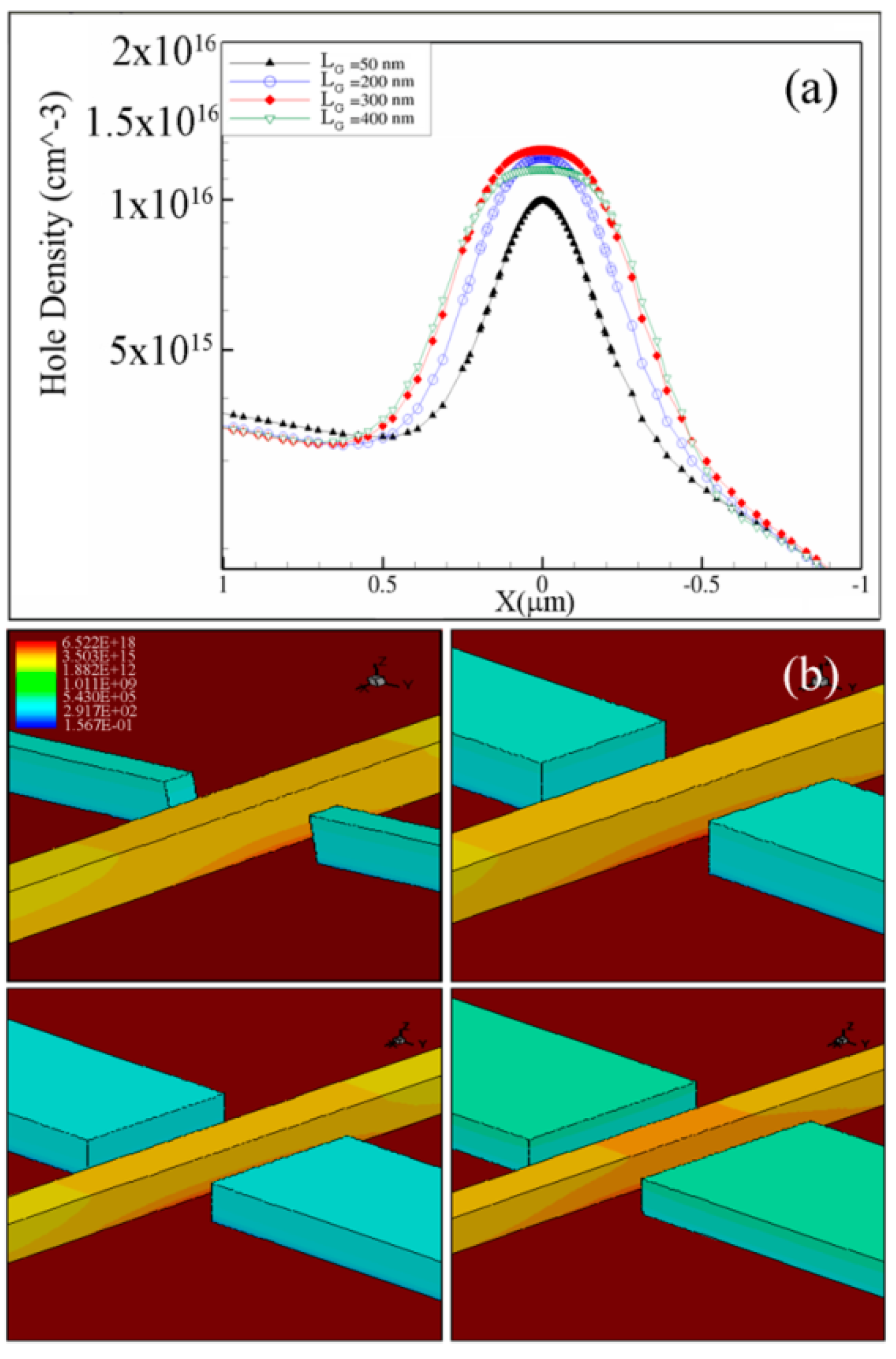
3.2.2. Accumulation Regime

To obtain a better insight into the effect of gate length variation on the performance of the device, the study is performed while the device is pushed into the accumulation region by applying a negative voltage to the lateral gates. The hole density distribution in devices with four different LG at a cutline along the channel of devices at the Z = 50 nm (AA’ In Figure 1a), and a side view of the same structures when the gate is biased by −2.0 V and drain is biased by −1.0 V are shown in Figure 7a,b respectively. As it is observed, by applying negative voltage to the lateral gates, majority carriers (holes) accumulate in the gated region and lead the device into accumulation mode. The accumulated holes in the channel vary the potential energy level in this region. On the other hand, hole concentration at the drain side of the gate is reduced significantly. This variation in the holes’ population happens in order to maintain the current continuity in this biasing condition. It can be concluded that the holes stored in the accumulation layer diffuse into the drain extension due to the hole density gradient, and then drift toward the drain contact, according to the electric field applied from it, where the holes finally reach saturation velocity. Even though, the hole velocity has its highest value at the drain region, reduction of the hole density can guarantee the current saturation.

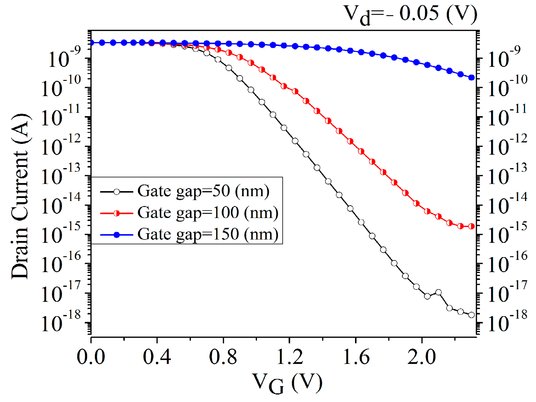
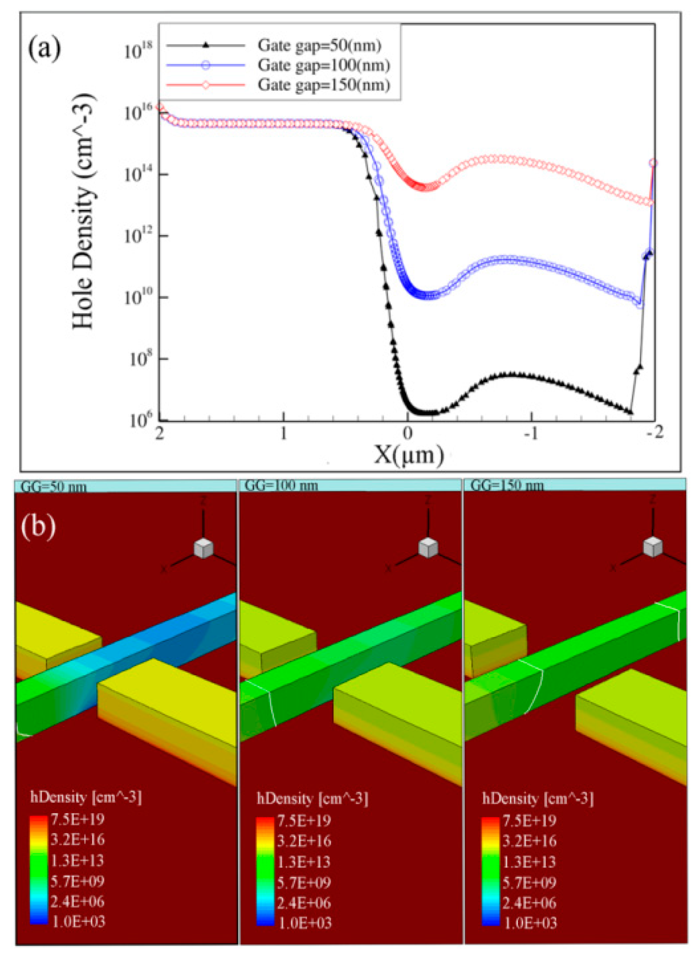
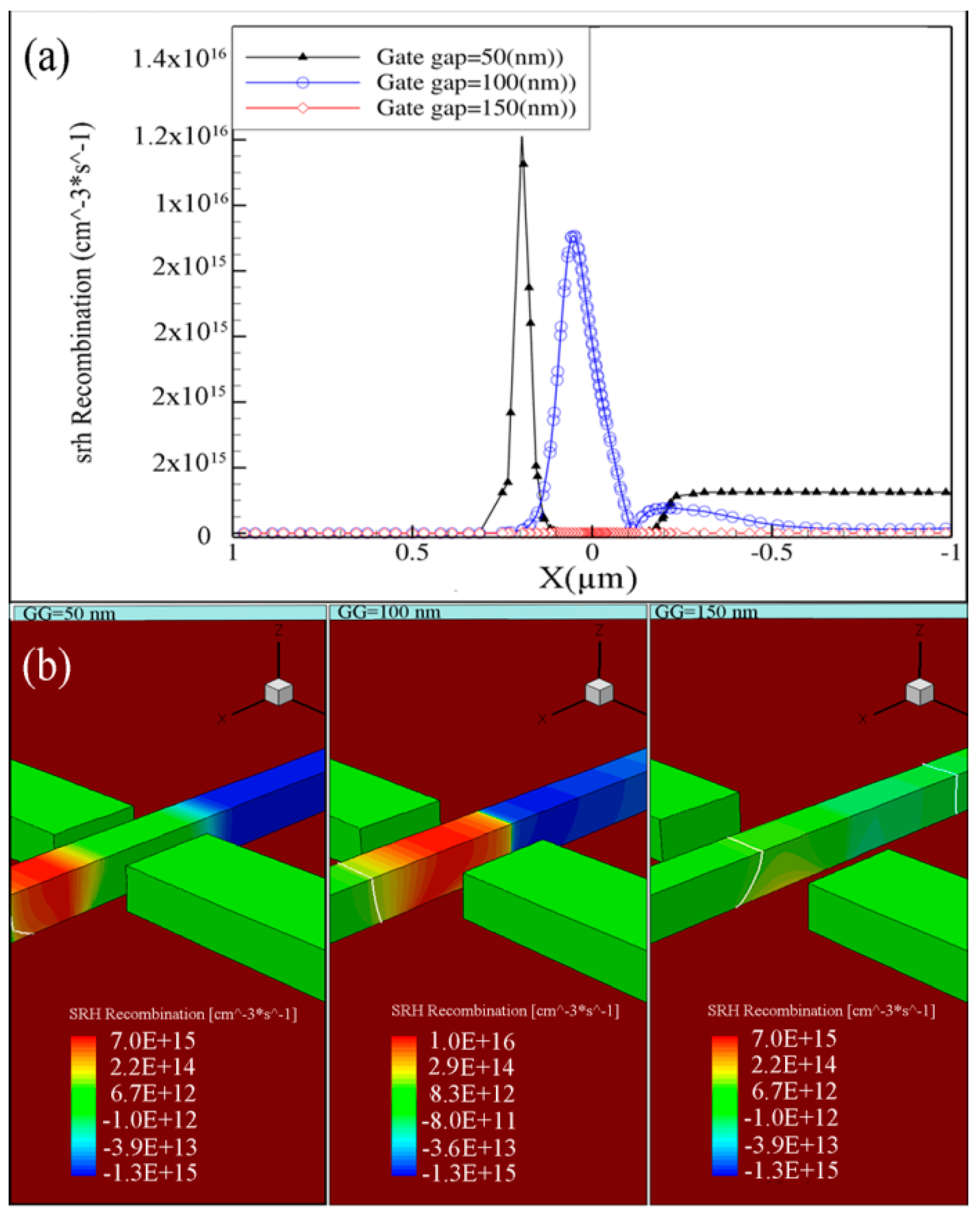
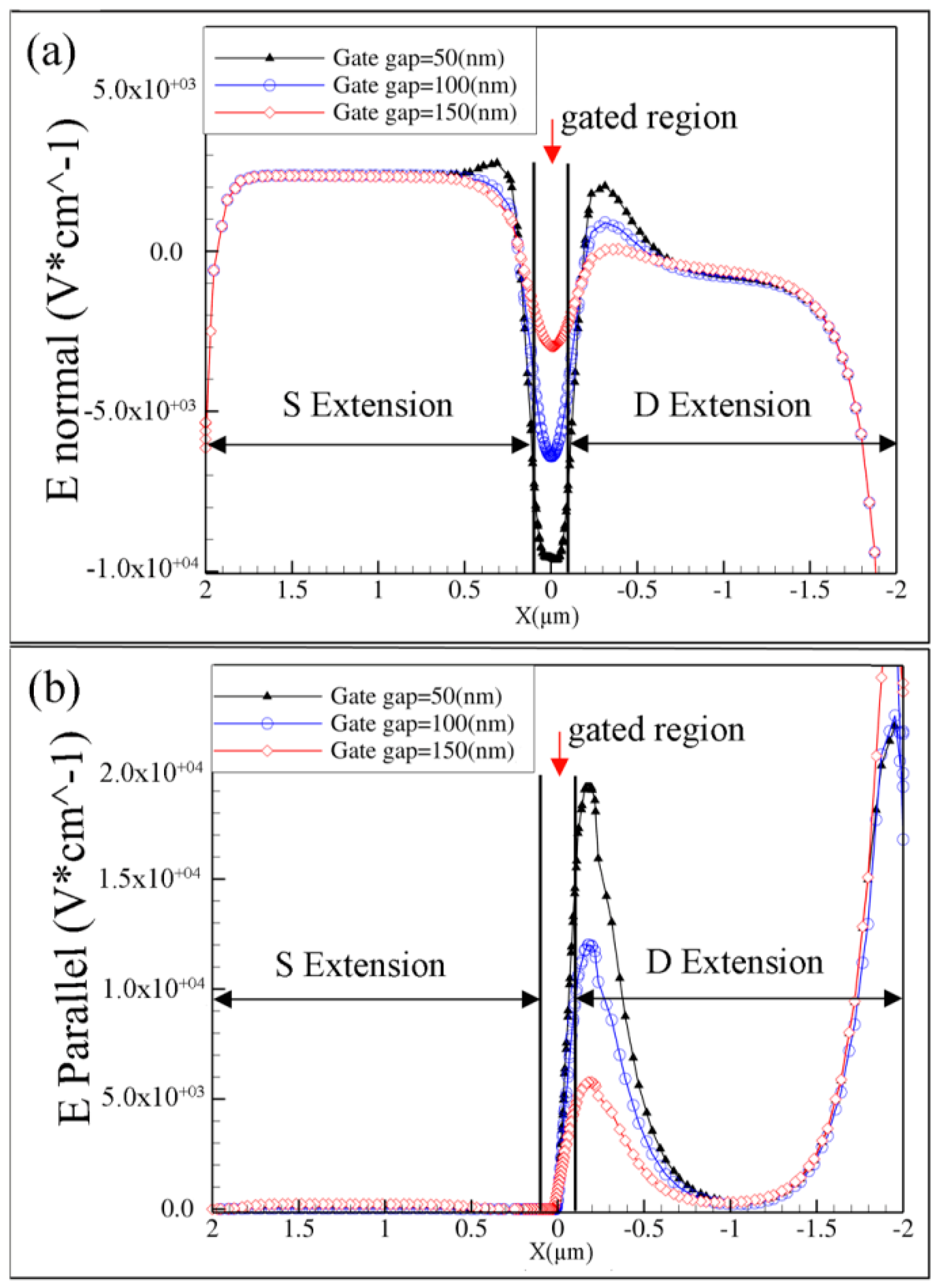
3.3. Effect of Gate Gap Variation

Another parameter of interest in this study is the variation of air gap between the lateral gates and channel and its effect on the performance of DGJLT device. Since the main operation of the device in between flatband and fully depleted region, the effect of gate gap is analysed just in the depletion region. Transfer characteristics of devices with three various gate gaps of 50, 100, and 150 nm at VG = +2 V and VD = −50 mV are presented in Figure 8. It indicates that the gap variation is an important parameter and plays critical role in modification of the device performance. The ON-state current remain almost unchanged for three devices; however, the OFF-state current decreased significantly in device with 50 nm gap.
In this device, compared to the device with 150-nm gate gap, a decrement of about eight orders of magnitude is obtained. This can make a lot of sense, since it indicates that, as the gap decreases and lateral gates come closer to the channel, the lateral gates’ influence on carriers is more pronounced. In this matter, the device with highest gate gap (150 nm) shows the poorest controllability of the lateral gates on channel with the lowest ON/OFF ratio. Although the entiredevices with different gate gaps are biased with high gate voltage, the threshold voltage is almost the same for three devices. If we compare the proposed structure with devices such as a-Si TFTs [46], with solid gate insulator, we note that at a high gate voltage, the threshold voltage shift is mainly due to the charge trapping in the insulator, while the breaking bonds in the channel or the creation of new states would be the dominant mechanisms in the low gate voltage regime [47]. In DGJLT, with the air gap and only one interface with the BOX at the bottom of the channel, the amount of charge trapping is negligible, and the threshold voltage shift would only be affected by the breaking of the bonds. Therefore, for the DGJLT devices with different gate gaps, the threshold voltage is approximately the same for all devices. Figure 9a,b present the hole concentration variation along a cutline at Z = 50 nm and side view of devices with different gate gaps of 50 nm, 100 nm and 150 nm. All the other parameters of the device are analogous to the reference nominated device. It indicates that the variation of gate gap affects the carriers’ distribution along the channel of the devices in the same quality that the channel geometry does. The hole density concentration shows a decrement of about ten orders of magnitude for device with 50 nm gate gap while it is just about two orders in devices with 150 nm gaps. The ambipolar behaviour is undesirable in all advanced transistors specially CMOS logic applications. As it can be observed in Figure 9a, in DGJLTs with various gate gaps when the device is in the OFF state, especially for device with a 50-nm gate gap, the majority carriers are depleted. At the same time, the simulation results reveal that the number of minority carriers in the channel is increased (not shown).
This depletion of majority carriers and accumulation of minority carriers can occur without any concern that the gated area be inverted, since the adjoining of the gated regions is also of the p-type (S/D extensions). Even if the gated area is inverted, the adjacent p-region with reverse bias originated from the drain voltage, would limit the transport of minority carriers in this region. These electrons can be recombined with the holes mainly in the source side of the gate. In order to examine the recombination rate of carriers, the SRH recombination rate for devices with various gate gaps at the pinch-off state is presented in Figure 10. As it is expected, the recombination rate of the device with a 50-nm gate gap was higher compared to the devices with a larger gate gap which confirms the latter discussion about the carrier recombination. It is worth to mention that the device with a 150-nm gate gap, simply begins to behave like a resistor. In this device, the gate loses the control over the carriers inside the channel which consequently causes a very low switching speed. It is predicted that at higher gate voltages, the 150-nm gate gap device also shows an acceptable switching speed and leakage current value, but that cannot work for our interest into the next generation of transistors with low power consumption.
Finally, the influence of air gap variation on electric field component is analysed. The normal and parallel components of electric field along a horizontal cut line at Z = 50 nm to the channel is presented in Figure 11a,b respectively. An improvement of 18% and 25% is observed in the strength of normal and parallel electric fields in the device with a 50 nm gap compared to the reference device with a 100-nm gap. The stronger normal electric field at the device with closer gate to the channel, more efficiently rearrange the carriers in the gated region compared to the devices with gates more far from the channel [48]. From the normal component of electric fields, it is noted that the source and the drain extension in the region close to the interface with the channel experience fringing field effect from the gate corners.
The effect of the fringing field is more pronounced in devices with a 50-nm gap and is diminished in devices with 150 nm gaps. The parallel component of electric field (Figure 11b) presents the expected behaviour of JLTs in which the peak of the electric field appears outside the channel region.

4. Conclusions

In this letter, we exploited the impact of two critical parameters associated with lateral gates on the performance of DGJLTs through 3D device simulation. The output characteristics of the device with variation of lateral gate length and air gate gap is analysed and discussed according to the behaviour of electric field component, carrier’s density inside the channel, band edge energies, and SRH recombination rate. It is found out that the lateral gate engineering will modify the performance of DGJLTs in the same quality as the channel geometry. By varying the lateral gate length in the range of 50–400 nm the subthreshold current varied by about six orders of magnitude while the ON-state current and threshold voltage remain constant. Moreover, it is concluded that, in DGJLTs with two lateral air gaps the design of gaps between lateral gates and channel, it is critically important to obtain the best performance of device. As the gates come closer to the channel, the switching speed of the device improves significantly due to the better electrostatic control of the gates over the carriers.

Author Contributions

F.L. and A.D. designed and performed the research and wrote the original draft manuscript. F.L. performed the computation. F.L., A.D., M.S.I. and H.Y.W. analysed the data. M.S.I., M.T.I. and H.Y.W. did Funding Acquisition. All authors discussed the results and commented on the manuscript.

Funding

This research was financially supported by the grant number MMUE180010 from TM R&D Malaysia.

Acknowledgments

The authors would like to thanks Iranian National Elites Foundation (130/2-925) and Iran national Science Foundation (98008756) for supporting this project.

Conflicts of Interest

The authors declare no conflict of interest.

References

  1. Lee, C.W.; Afzalian, A.; Akhavan, N.D.; Yan, R.; Ferain, I.; Colinge, J.P. Junctionless multigate field-effect transistor. Appl. Phys. Lett. 2009, 94, 053511–053511-2. [Google Scholar] [CrossRef]
  2. Colinge, J.P.; Lee, C.W.; Afzalian, A.; Akhavan, N.D.; Yan, R.; Ferain, I.; Razavi, P.; O’Neill, B.; Blake, A.; White, M. Nanowire transistors without junctions. Nat. Nanotechnol. 2010, 5, 225–229. [Google Scholar] [CrossRef] [PubMed]
  3. Doria, R.T.; Trevisoli, R.; de Souza, M.; Pavanello, M.A. Low-frequency noise and effective trap density of short channel p-and n-types junctionless nanowire transistors. Solid-State Electron. 2014, 96, 22–26. [Google Scholar] [CrossRef]
  4. Colinge, J.P.; Ferain, I.; Kranti, A.; Lee, C.W.; Akhavan, N.D.; Razavi, P.; Yan, R.; Yu, R. Junctionless Nanowire Transistor: Complementary Metal-Oxide-Semiconductor Without Junctions. Sci. Adv. Mater. 2011, 3, 477–482. [Google Scholar] [CrossRef]
  5. Jang, D.; Lee, J.W.; Lee, C.W.; Colinge, J.P.; Montès, L.; Lee, J.I.; Kim, G.T.; Ghibaudo, G. Low-frequency noise in junctionless multigate transistors. Appl. Phys. Lett. 2011, 98, 133502. [Google Scholar] [CrossRef] [Green Version]
  6. Han, M.-H.; Chang, C.-Y.; Chen, H.-B.; Wu, J.-J.; Cheng, Y.-C.; Wu, Y.-C. Performance comparison between bulk and SOI junctionless transistors. IEEE Electron Device Lett. 2013, 34, 169–171. [Google Scholar] [CrossRef]
  7. Gundapaneni, S.; Konar, A.; Bajaj, M.; Murali, K. Improved Performance of Junctionless Tunnel FETs with Source/Channel Heterostructure. In Physics of Semiconductor Devices; Springer: Berlin/Heidelberg, Germany, 2014; pp. 289–290. [Google Scholar]
  8. Colinge, J.; Kranti, A.; Yan, R.; Lee, C.; Ferain, I.; Yu, R.; Akhavan, N.D.; Razavi, P. Junctionless nanowire transistor (JNT): Properties and design guidelines. Solid-State Electron. 2011, 65, 33–37. [Google Scholar] [CrossRef]
  9. Chung, C.C.-C.; Shen, C.-H.; Lin, J.-Y.; Chin, C.-C.; Chao, T.-S. Vertically stacked cantilever n-type poly-Si junctionless nanowire transistor and its series resistance limit. IEEE Trans. Electron Devices 2018, 65, 756–762. [Google Scholar] [CrossRef]
  10. Ma, L.; Han, W.; Wang, H.; Yang, X.; Yang, F. Observation of degenerate one-dimensional subbands in single n-channel junctionless nanowire transistors. IEEE Electron Device Lett. 2015, 36, 941–943. [Google Scholar]
  11. Konar, A.; Mathew, J.; Nayak, K.; Bajaj, M.; Pandey, R.K.; Dhara, S.; Murali, K.; Deshmukh, M.M. Carrier transport in high mobility InAs nanowire junctionless transistors. Nano Lett. 2015, 15, 1684–1690. [Google Scholar] [CrossRef]
  12. Chen, L.; Cai, F.; Otuonye, U.; Lu, W.D. Vertical Ge/Si core/shell nanowire junctionless transistor. Nano Lett. 2015, 16, 420–426. [Google Scholar] [CrossRef] [PubMed]
  13. Cao, W.; Kang, J.; Banerjee, K. Junction-Less Monolayer MoS2 FETs. arXiv 2015, arXiv:1509.00561. [Google Scholar]
  14. Mirabelli, G.; Duffy, R.; Hurley, P.; Monaghan, S.; Cherkaoui, K.; Schmidt, M.; Sheehan, B.; Povey, I.M.; McCarthy, M.; Nagle, R. Mo-Based Transition-Metal-Dichalcogenide Junctionless Field-Effect-Transistors; Meeting Abstracts; The Electrochemical Society: San Diego, CA, USA, 2016; p. 1289. [Google Scholar]
  15. Faraji, M.; Ghoreishi, S.S.; Yousefi, R. Gate structural engineering of MOS-like junctionless Carbon nanotube field effect transistor (MOS-like J-CNTFET). Int. J. Nano Dimens. 2018, 9, 32–40. [Google Scholar]
  16. Cheng, P.-H.; Wang, C.-Y.; Chang, T.-J.; Shen, T.-H.; Cai, Y.-S.; Chen, M.-J. Room-temperature field effect transistors with metallic ultrathin TiN-based channel prepared by atomic layer delta doping and deposition. Sci. Rep. 2017, 7, 875. [Google Scholar] [CrossRef] [PubMed]
  17. Narang, R.; Saxena, M.; Gupta, M. Investigation of dielectric modulated (DM) double gate (DG) junctionless MOSFETs for application as a biosensors. Superlattices Microstruct. 2015, 85, 557–572. [Google Scholar]
  18. Pratap, Y.; Kumar, M.; Kabra, S.; Haldar, S.; Gupta, R.; Gupta, M. Analytical modeling of gate-all-around junctionless transistor based biosensors for detection of neutral biomolecule species. J. Comput. Electron. 2018, 17, 288–296. [Google Scholar] [CrossRef]
  19. Chen, X. Biodegradable Junctionless Transistors with Extremly Simple Structure. IEEE Electron Device Lett. 2015, 36, 908–910. [Google Scholar]
  20. Bartsch, S.T.; Arp, M.; Ionescu, A.M. Junctionless Silicon Nanowire Resonator. IEEE J. Electron Devices Soc. 2014, 2, 8–15. [Google Scholar] [CrossRef] [Green Version]
  21. Vaurette, F.; Leturcq, R.; Lepilliet, S.; Grandidier, B.; Stiévenard, D. Confinement-modulated junctionless nanowire transistors for logic circuits. Nanoscale 2014, 6, 13446–13450. [Google Scholar] [CrossRef]
  22. Roudsari, A.F.; Khodadadzadeh, I.; Saini, S.S.; Anantram, M. Junction-less nanowire based photodetector: Role of nanowire width. arXiv 2017, arXiv:1707.07892. [Google Scholar]
  23. Chang, M.S.; Cheung, R.W. Method of Decreased Interlayer Dielectric Constant in a Multilayer Interconnect Structure to Increase Device Speed Performance. US5559055A, 24 September 1996. [Google Scholar]
  24. Kocon, C.B.; Elbanhawy, A. Method and Apparatus for Improved MOS Gating to Reduce Miller Capacitance and Switching Losses. US6870220B2, 22 March 2005. [Google Scholar]
  25. Park, J.M. Improving CMOS Speed and Switching Power with Air-Gap Structures; No. UCB/EECS-2011-84; UC Berkeley: Berkeley, CA, USA, 2011. [Google Scholar]
  26. Rabaey, J.M.; Pedram, M. Low Power Design Methodologies; Spring Science + Business Media: New York, NY, USA, 1996. [Google Scholar]
  27. Grill, A.; Gates, S.M.; Ryan, T.E.; Nguyen, S.V.; Priyadarshini, D. Progress in the development and understanding of advanced low k and ultralow k dielectrics for very large-scale integrated interconnects—State of the art. Appl. Phys. Rev. 2014, 1, 011306. [Google Scholar] [CrossRef] [Green Version]
  28. Triyoso, D.; Mulfinger, G.; Hempel, K.; Tao, H.; Koehler, F.; Kang, L.; Kumar, A.; McArdle, T.; Holt, J.; Child, A. Characterization of atomic layer deposited low-k spacer for FDSOI high-k metal gate transistor. In Proceedings of the 2017 IEEE International Conference on IC Design and Technology (ICICDT), Austin, TX, USA, 23–25 May 2017; pp. 1–4. [Google Scholar]
  29. Yang, T.; Mehta, J.S.; Mativetsky, J.M. An air gap moderates the performance of nanowire array transistors. Nanotechnology 2017, 28, 125204. [Google Scholar] [CrossRef]
  30. Mativetsky, J.; Yang, T.; Mehta, J. Impact of the air gap in nanowire array transistors. In Proceedings of the APS Meeting Abstracts, 2017, New Orleans, LA, USA, 13–17 March 2017. [Google Scholar]
  31. Shin, S.-H.; Ji, S.; Choi, S.; Pyo, K.-H.; An, B.W.; Park, J.; Kim, J.; Kim, J.-Y.; Lee, K.-S.; Kwon, S.-Y. Integrated arrays of air-dielectric graphene transistors as transparent active-matrix pressure sensors for wide pressure ranges. Nat. Commun. 2017, 8, 14950. [Google Scholar] [CrossRef] [PubMed]
  32. Abadeer, W.W.; Chatty, K.V.; Gauthier, R.J., Jr.; Rankin, J.H.; Tonti, W.R.; Shi, Y. Field Effect Transistor with Air Gap Dielectric. US8349697B2, 18 October 2012. [Google Scholar]
  33. Sachid, A.B.; Huang, Y.-M.; Chen, Y.-J.; Chen, C.-C.; Lu, D.D.; Chen, M.-C.; Hu, C. FinFET withencased air-gap spacers for high-performance and low-energy circuits. IEEE Electron Device Lett. 2017, 38, 16–19. [Google Scholar] [CrossRef]
  34. Dehzangi, A.; Abdullah, A.M.; Larki, F.; Hutagalung, S.D.; Saion, E.B.; Hamidon, M.N.; Hassan, J.; Gharayebi, Y. Electrical property comparison and charge transmission in p-type double gate and single gate junctionless accumulation transistor fabricated by AFM nanolithography. Nanoscale Res. Lett. 2012, 7, 1–9. [Google Scholar] [CrossRef] [PubMed]
  35. Larki, F.; Dehzangi, A.; Saion, E.B.; Abedini, A.; Hutagalung, S.D.; Abdullah, A.M.; Hamidon, M.N. Simulation of transport in laterally gated junctionless transistors fabricated by local anodization with an atomic force microscope. Phys. Status Solidi A 2013, 210, 1914–1919. [Google Scholar] [CrossRef]
  36. Dehzangi, A.; Larki, F.; Hutagalung, S.D.; Naseri, M.G.; Majlis, B.Y.; Navasery, M.; Hamid, N.A.; Noor, M.M. Impact of Parameter Variation in Fabrication of Nanostructure by Atomic Force Microscopy Nanolithography. PLoS ONE 2013, 8, e65409. [Google Scholar] [CrossRef] [PubMed]
  37. Larki, F.; Dehzangi, A.; Ali, S.H.M.; Jalar, A.; Islam, M.S.; Hamidon, M.N.; Majlis, B.Y. Effect of Geometric Parameters on the Performance of P-Type Junctionless Lateral Gate Transistors. PLoS ONE 2014, 9, e95182. [Google Scholar] [CrossRef]
  38. Larki, F.; Dehzangi, A.; Abedini, A.; Abdullah, A.M.; Saion, E.; Hutagalung, S.D.; Hamidon, M.N.; Hassan, J. Pinch-off mechanism in double-lateral-gate junctionless transistors fabricated by scanning probe microscope based lithography. Beilstein J. Nanotechnol. 2012, 3, 817–823. [Google Scholar] [CrossRef] [Green Version]
  39. Dehzangi, A.; Larki, F.; Md Ali, S.H.; Hutagalung, S.D.; Islam, S.; Hamidon, M.N.; Menon, S.; Jalar, A.; Hassan, J.; Yeop Majlis, B. Study of the side gate junctionless transistor in accumulation region. Microelectron. Int. 2016, 33, 61–67. [Google Scholar] [CrossRef]
  40. Larki, F.; Dehzangi, A.; Islam, M.S.; Ali, S.H.M.; Abedini, A.; Majlis, B. Effect of Channel Width Variation on Electrical Characteristics of Double Lateral Gate Junctionless Transistors; A Numerical Study. Silicon 2018, 10, 1305–1314. [Google Scholar] [CrossRef]
  41. Sentaurus, T. User Guide; Synopsys Inc.: Mountain View, CA, USA, 2010. [Google Scholar]
  42. Tsai, M.-J.; Chiang, Y.-Y.; Lin, Y.-R.; Kurniawan, E.D.; Wu, Y.-C. Hybrid N-Type Poly-Si Ultra-Thin Nanowire Shell Channel with P-Substrate Structure by Electron Beam Lithography Adjustment for Junctionless Field-Effect Transistors. ECS J. Solid State Sci. Technol. 2018, 7, Q201–Q205. [Google Scholar] [CrossRef]
  43. Liu, C.; Cheng, C.-H.; Lin, M.-H.; Shih, Y.-J.; Hung, Y.-W.; Fan, C.-C.; Chen, H.-H.; Chen, W.-H.; Hsu, C.-C.; Shih, B.-Y. Improved Thermal Stability and Stress Immunity in Highly Scalable Junctionless FETs Using Enhanced-Depletion Channels. ECS J. Solid State Sci. Technol. 2018, 7, Q242–Q245. [Google Scholar] [CrossRef]
  44. Cho, W.-J. Characterizations of interface-state density between top silicon and buried oxide on Nano-SOI substrate by using pseudo-MOSFETs. JSTS J. Semicond. Technol. Sci. 2005, 5, 83–88. [Google Scholar]
  45. Pai, C.-Y.; Lin, J.-T.; Wang, S.-W.; Lin, C.-H.; Kuo, Y.-S.; Eng, Y.-C.; Lin, P.-H.; Fan, Y.-H.; Tai, C.-H.; Chen, H.-H. Numerical study of performance comparison between junction and junctionless thin-film transistors. In Proceedings of the 2010 10th IEEE International Conference on Solid-State and Integrated Circuit Technology, Shanghai, China, 1–4 November 2010; pp. 1410–1412. [Google Scholar]
  46. Powell, M. Charge trapping instabilities in amorphous silicon-silicon nitride thin-film transistors. Appl. Phys. Lett. 1983, 43, 597–599. [Google Scholar] [CrossRef]
  47. Deane, S.; Wehrspohn, R.; Powell, M. Unification of the time and temperature dependence of dangling-bond-defect creation and removal in amorphous-silicon thin-film transistors. Phys. Rev. Ser. B 1998, 58, 12625–12628. [Google Scholar] [CrossRef]
  48. Larki, F.; Dehzangi, A.; Ali, S.H.M.; Jalar, A.; Islam, M.; Majlis, B.Y.; Saion, E.B.; Hamidon, M.N.; Hutagalung, S.D. Dependency of electrical characteristics on nano gap variation in pinch off lateral gate transistors. In Proceedings of the 2014 IEEE International Conference on Semiconductor Electronics (ICSE), Kuala Lumpur, Malaysia, 27–29 August 2014; pp. 170–173. [Google Scholar]
Figure 1. (a) Isotropic views and (b) top view of a nominal p-type double lateral gate junctionless transistors (DGJLT).
Electronics 08 00538 g001
Figure 2. The transfer characteristics of the devices with lateral gate length of 50, 200, 300, and 400 nm when the gate voltage varied from 0 V to +2.0 V and VD = −1.0 V.
Electronics 08 00538 g002
Figure 3. Components of electric field distribution along a horizontal cut line at the center of the channel (Z = 50 nm), (a) along X-axis (b) along Y-axis (c) along Z-axis (d) superposition of electric field components.
Electronics 08 00538 g003
Figure 4. (a)The variation of valence band edge energy and (b) electrostatic potential from the source to the drain contact for different LG, at VD = −1 V and VG = +2 V.
Electronics 08 00538 g004
Figure 5. (a) Holes distribution along the channel for the devices with four different LGs at the cutline of Z = 50 nm, (b) the corresponding side views of the holes (c) electrons distribution along the channel for the same devices with four LGs at a cutline at Z = 50 nm, and (d) the corresponding side view of the electron distribution.
Electronics 08 00538 g005
Figure 6. (a) The SRH recombination–generation rate along a cutline at Z = 50 nm and (b) a bird eye view for devices with different LG for a VG = +2 V and = VD = −1 V.
Electronics 08 00538 g006
Figure 7. (a)Hole density distribution along the channel of devices with four LG at a cutline at Z = 50 nm and (b) side view of hole density distribution at VG = −2.0 V and VD = −1.0 V.
Electronics 08 00538 g007
Figure 8. Output characteristics comparison of three devices with 50, 100 and 150 nm gate gap.
Electronics 08 00538 g008
Figure 9. (a) Holes density distribution along the channel for the devices with three different gate gaps of 50 nm, 100 nm, and 100 nm at a cutline at Z = 50 nm, and (b) the corresponding side views of the holes inside the device at VD = −1.0 V and VG = +2.0 V.
Electronics 08 00538 g009
Figure 10. (a) The SRH recombination–generation rate along a cutline at Z = 50 nm and (b) a bird eye view for devices with different gate gap at VG = +2 V and VD =−1 V.
Electronics 08 00538 g010
Figure 11. The electric field affected on the majority carriers along a horizontal cut line at Z = 50 nm in direction (a) perpendicular and (b) parallel to the channel.
Electronics 08 00538 g011
Table 1. Process/device parameters.
Parameter Value
Gate length (LG)50, 200, 300, 400 nm
Gate Gap (GG)50, 100, 150 nm
Contact work function5.12 eV
Gate voltage−2 V to +2 V
Drain Voltage−0.05 V to −1 V

