Article

A Current Reconstruction at Parallel Three Phase Inverters Using Two Current Sensors

Department of Electrical Engineering, Konkuk University, Seoul 05029, Korea
*
Author to whom correspondence should be addressed.
Electronics 2019, 8(2), 179; https://doi.org/10.3390/electronics8020179
Submission received: 18 November 2018 / Revised: 28 January 2019 / Accepted: 31 January 2019 / Published: 4 February 2019
(This article belongs to the Special Issue Renewable Electric Energy Systems)

Abstract

:
In this paper, a current restoration method which can be applied to three phase parallel interleaved inverters (TPPII) using two current sensors has been proposed. In the proposed current reconstruction method, the branch current and the phase current of the two phases of the TPPII are sampled concurrently at the peak and valley of the pulse width modulation (PWM) carrier using two hall-effect sensors. Then, the phase current of each inverter is reconstructed by analyzing the sensed current with the current conduction path information according to the switch state in the peak and valley of the PWM carrier. This paper additionally analyzes the characteristics of the offset occurring in the detection process of two current sensors and it proposes a compensation method to reduce the offset on-line. In order to at once reduce the offset of the three-phase recovery current caused by the DC offset of the sensor, a coordinate conversion method and a low pass are used. To verify the performance of the proposed current recovery method and real-time offset compensation method, a simulation using PSIM software was performed, and experiments were conducted using a three phase parallel inverter composed of insulated gate bipolar transistor (IGBT) modules. In particular, the AC offset that occurred in the sampling process during the experiment was analyzed and modeled, and it was reduced by simple calculation.

1. Introduction

TPPII is widely used in large-capacity energy storage system (ESS), uninterruptible power supply (UPS) and motor drive applications [1,2,3,4]. Generally, to control the current of TPPII, the output current that composes each inverter’s phase current is detected [5]. However, if the output filter of the three-phase inverter is not the same, there is a difference in the phase current of each inverter, and this differential current makes current control difficult. Moreover, the current capacity of the inverters can be lower since the differential current causes imbalance losses between the parallel inverters. To solve this problem, a method of detecting and controlling each phase current of the inverter module is required. It is possible to get the phase current information using multiple current sensors, such as those shown in Figure 1 [6]. However, in the case of Figure 1, the analog to digital converter (ADC) circuits are required in order to obtain as many sensor outputs as sensor numbers. Furthermore, the price is increased because of the number of sensors and the ADC circuits. In addition, if multiple sensors are used, the gain and offset are different for each sensor, so more effort is required to compensate for the gain and offset. In order to solve problems when using multiple sensors, many methods have been proposed for reconstructing the current of a three-phase inverter using a single sensor. A method of reconstructing the three-phase current is proposed in [7], it takes into account the DC-link current sampled by a single current sensor and the switch state. However, when the switching vector exists within a short period of time in the PWM period, there is a dead zone in which it is difficult to recover the phase current by using the DC-link current and the state information of the switch. In [8], when the dead zone occurs according to the switching state, the minimum voltage vector is injected and compensated to expand the measurement boundary. In [9], the modified voltage vector and observer were used to improve the reconstruction performance in the dead zone region. In addition, [10] proposed a current reconstruction algorithm in order to reconstruct on a low modulation index region. Moreover, an algorithm has been proposed to minimize the reduction of the control performance due to the inaccuracy of the current reconstruction in [11,12]. Furthermore, a study on compensating the current reconstruction performance using the DC-link current information exists in order to estimate the phase current through the load model [13]. In addition to this, the algorithm for a current sensor offset was proposed in [14]. In [15,16], the current reconstruction method is addressed via a multilevel inverter. The jitter-like wave form in a reconstructed current is reduced in [17]. However, the above-mentioned methods require machine model information that is difficult to actually measure, or a complicated vector injection method. In particular, if the information of the mechanical model is wrong, the error of the restored current can be further increased. Furthermore, the aforementioned methods do not address the offset problem of the sensor.
Meanwhile, the current reconstruction method of a three-phase inverter via the use of a single sensor has been proposed [18]. This method can reconstruct a three-phase current by detecting the branch current and phase current of the inverter in the zero voltage vector, dramatically reducing the dead zone.
This paper describes the current reconstruction and offset compensation strategy in TPPII, utilizing the method in [18]. Therefore, it simultaneously presents both the advantages and disadvantages that exist in [18]. It is possible to restore all phase currents of TPPII with only two current sensors. However, in order to concurrently measure the phase current and the branch current in the peak and valley of the PWM carrier of the TPPII, a hall-effect current sensor having a high bandwidth is required. Meanwhile, in contrast to the DC-link voltage of 12 V in [18], in this paper we verified the applicability of the proposed algorithm in a grid connection system and motor drive application by increasing the DC-link voltage to 425 V and the output voltage to 110 V. Furthermore, the DC and AC offset of the reconstructed current are analyzed in a stationary reference frame and synchronous reference frame. In addition, using simple transformation and digital filter, the accuracy of the current reconstruction is improved. Finally, the simulation and experimental results are demonstrated.

2. Proposed Current Reconstruction and Offset Compensation Method

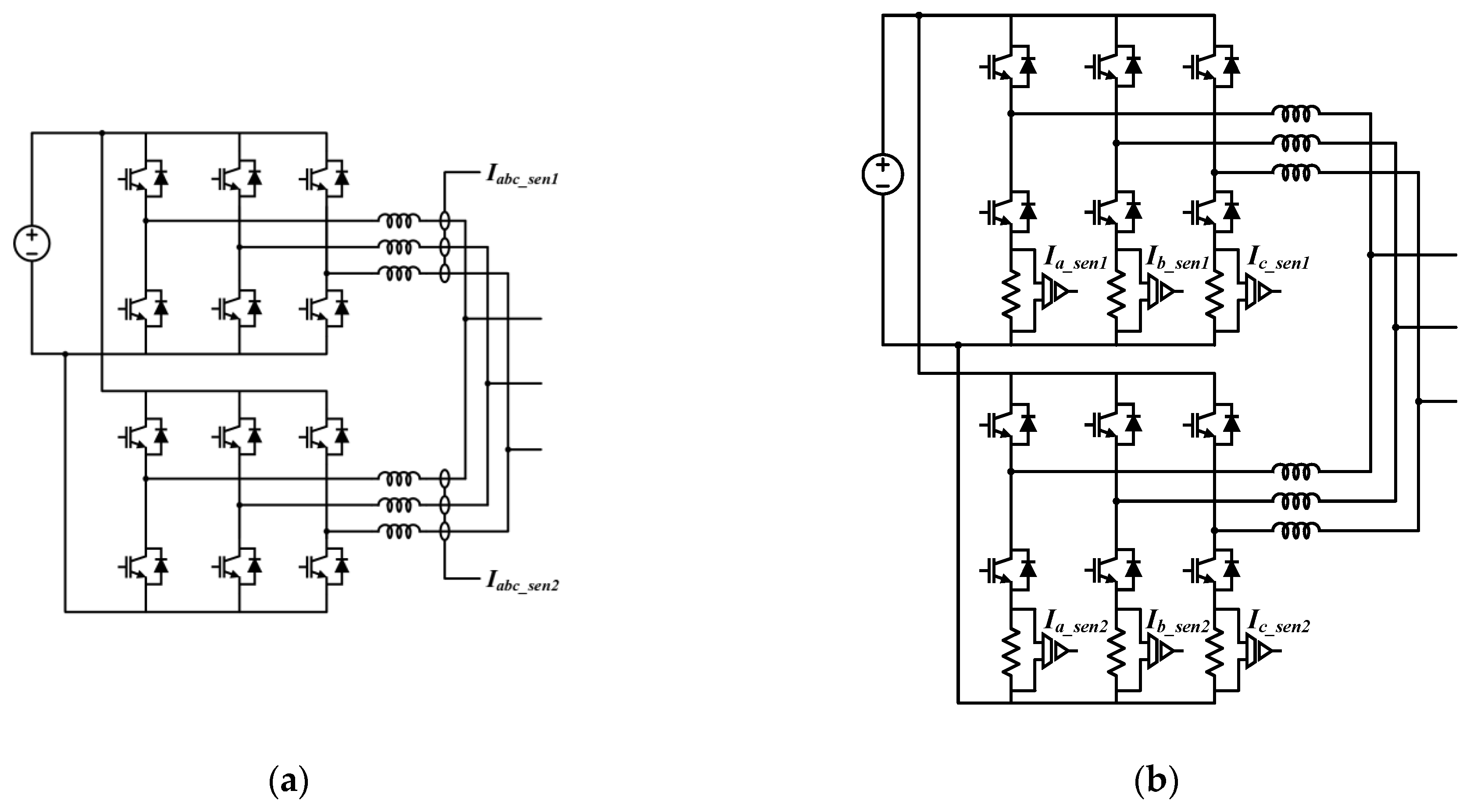
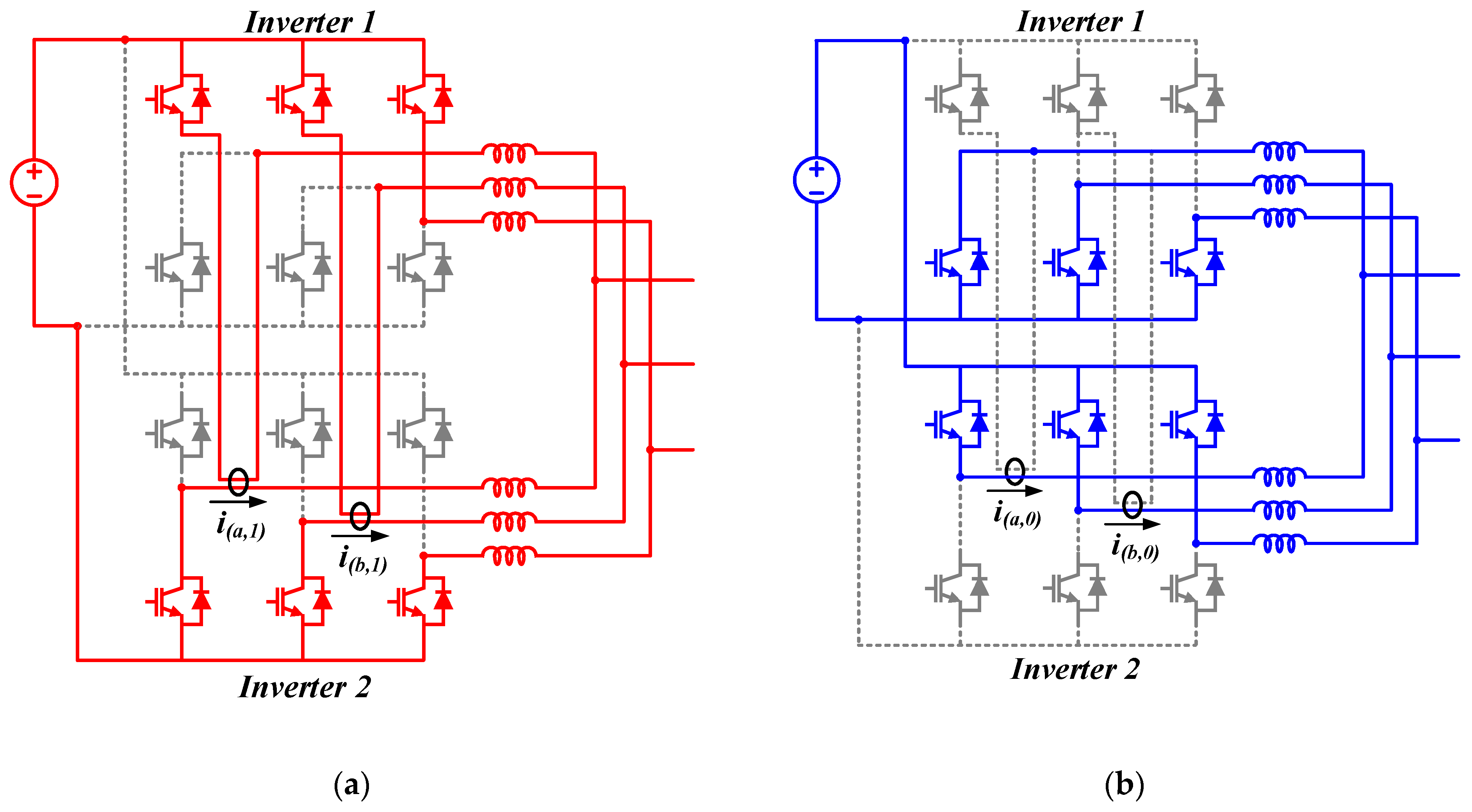
2.1. Current Detection and Reconstruction Method

In this paper, a current reconstruction method for TPPII is proposed. In order to explain the proposed current reconstruction method, the current path according to the switch state of TPPII is shown in Figure 2. Moreover, the relationship of the sampling points and switch states is illustrated in Figure 3a. Following this, the proposed current reconstruction algorithm is depicted in Figure 3b.
The proposed method simultaneously detects the branch current of inverter 1 and phase current of inverter 2, as shown in Figure 2. The current is sampled once at the valley and peak of the PWM carrier in one switching period, as shown in Figure 3. In this way, the current information combined by one branch current and one phase current can be sampled at the (1, 1, 1) vector of the inverter 1, and one phase current information can be obtained at the (0, 0, 0) vector of inverter 2. Therefore, by using the current information obtained from each sampling point using one current sensor, one can obtain the phase current information of inverters 1 and 2 within one switching period. In the same way, if a second current sensor is used, the current of another phase can also be restored. Finally, the current information of the other phase can be known from the two reconstructed phase currents. Therefore, by restoring each phase current of TPPII using two current sensors, the proposed method can reduce the number of sensors and ADC circuits when compared to the current detection method that uses multiple current sensors (shown in Figure 1).
The above-mentioned current restoration method is formally analyzed as follows. The current detected in (0, 0, 0) of inverter 1 is the phase A current of inverter 2. On the other hand, the current detected in (1, 1, 1) of inverter 1 is composed of the phase A branch current of inverter 1 and phase A current of inverter 2. Therefore, the current detected in each vector can be expressed by the Equations (1) and (2). In Equations (1) and (2), i(a,0) and i(a,1) are the sampled currents in the zero vectors of the inverter 1.
i ( a , 0 ) = i a 2
i ( a , 1 ) = i a 1 + i a 2
If the phase inductors of the parallel inverters are large enough, so that the average inductor current change between (0, 0, 0) and (1, 1, 1) is not large, the ia2 detected between (0, 0, 0) and (1, 1, 1) can be assumed to be the same. Therefore, the reconstructed phase A current of inverter 1 ia1_re and reconstructed phase A current of inverter 2 ia2_re can be expressed by Equations (3) and (4).
i a 2 _ r e = i ( a , 0 ) = i a 2
i a 1 _ r e = i ( a , 1 ) i ( a , 0 ) = i a 1
Using the same principle, the reconstructed phase B current of each inverter can be expressed by Equations (5) and (6). Furthermore, the reconstructed phase C current of each inverter is given by Equations (7) and (8).
i b 2 _ r e = i ( b , 0 ) = i b 2
i b 1 _ r e = i ( b , 1 ) i ( b , 0 ) = i b 1
i c 2 _ r e = ( i a 2 _ r e + i b 2 _ r e ) = ( i a 2 + i b 2 )
i c 1 _ r e = ( i a 1 _ r e + i b 1 _ r e ) = ( i a 1 + i b 1 )

2.2. DC Offset in Reconstructed Current Compensation

In the current reconstruction method, an offset error caused by the sensor and hardware circuit can occur. By using the same sensor as illustrated in Figure 2, the detected current in (0, 0, 0) vector i(a,0) and current in (1, 1, 1) vector i(a,1) have the same error. Hence, the detected current i(a,0) and i(a,1) with DC offset Ioff_a can be written as follows:
i ( a , 0 ) = i a 2 + I o f f _ a
i ( a , 1 ) = i a 1 + i a 2 + I o f f _ a
Using the same principle, the detected current i(b,0) and i(b,1) with DC offset Ioff_b can be expressed as:
i ( b , 0 ) = i b 2 + I o f f _ b
i ( b , 1 ) = i b 1 + i b 2 + I o f f _ b
By considering the above equation, the reconstructed phase current for each inverter can be written as below:
i a 2 _ r e = i ( a , 0 ) = i a 2 + I o f f _ a
i a 1 _ r e = i ( a , 1 ) i ( a , 0 ) = i a 1
i b 2 _ r e = i ( b , 0 ) = i b 2 + I o f f _ b
i b 1 _ r e = i ( b , 1 ) i ( b , 0 ) = i b 1
i c 2 _ r e = ( i a 2 _ r e + i b 2 _ r e )   = ( i a 2 + i b 2 + I o f f _ a + I o f f _ b )
i c 1 _ r e = ( i a 1 _ r e + i b 1 _ r e ) = ( i a 1 + i b 1 )
It should be noted that there is no offset on the reconstructed phase currents in inverter 1, but the reconstructed currents of inverter 2 contain DC offset components.
To compensate for the offset components, using Clark’s Transformation and Equations (13), (15), and (17), the current i α and i β in α β -stationary reference frame is defined as below:
( i α i β ) = ( i a 2 + I o f f _ a i b 2 i c 2 3 + I o f f _ a + 2 I o f f _ b 3 ) = ( i α i β ) + ( I o f f _ α I o f f _ β )
where i α and i β are the fundamental α β -stationary reference frame currents, and I o f f _ α and I o f f _ β are the offset components in the α β -stationary reference frame.
Furthermore, Equation (19) can be transformed by Park’s transformation as follows:
( i d i q ) = ( cos θ sin θ sin θ cos θ ) ( i α i β ) + ( cos θ sin θ sin θ cos θ ) ( I o f f _ α I o f f _ β )
where θ is the reference angle of the inverter, and i d and i q are the d q -synchronous reference frame currents.
Given that i α and i β are fundamental α β -stationary reference frame currents, the first term on the right side of Equation (20) can be considered as DC components. The other side, I o f f _ α and I o f f _ β , are DC offset components; therefore, the second term on the right side of Equation (20) is AC ripple components. Hence, the DC offset of the sensor and hardware circuit can be considered as AC ripple components in a d q -synchronous reference frame. These AC ripple components can be simply eliminated by using a digital low pass filter:
( i d i q ) = ( cos θ sin θ sin θ cos θ ) ( i α i β )
Equation (21) represent Equation (20) with a low pass filter, where i d and i q are ideal d q -synchronous reference frame currents. Equation (21) can be inversely transformed from d q -synchronous coordinates to obtain a b c coordinates. In conclusion, the current can be reconstructed without a DC offset.

3. Simulation Results

By using a PSIM simulation program, the proposed current construction method is verified via the TPPII, which operates in open-loop. Table 1 represents the simulation condition. In the simulation, TPPII has R-load and is run as voltage source inverter (VSI). In addition, a switching frequency that is generally available in a large capacity power conversion system using an IGBT module is used. Furthermore, as mentioned in Section 2, TPPII has enough phase filter inductors to reduce the average current variation within one switching period.
In Figure 4, the actual and sampled current of the inverter 1 are depicted. The phase currents ia1 and ia2 are the phase currents of the parallel inverters, and ismp is the sampled current. ismp only contains ia2 current components at the (0, 0, 0) vector of the inverter 1. On the other hands, ismp contains the summation of ia1 and ia2 at the (1, 1, 1) vector of the inverter 1.
In Figure 5a, ix1 and ix1_re (x = a, b, c) represent the actual current and the reconstructed current of the inverter 1. Also, ix2 and ix2_re (x = a, b, c) state the actual current and the reconstructed current of the inverter 2, as shown in Figure 5b.

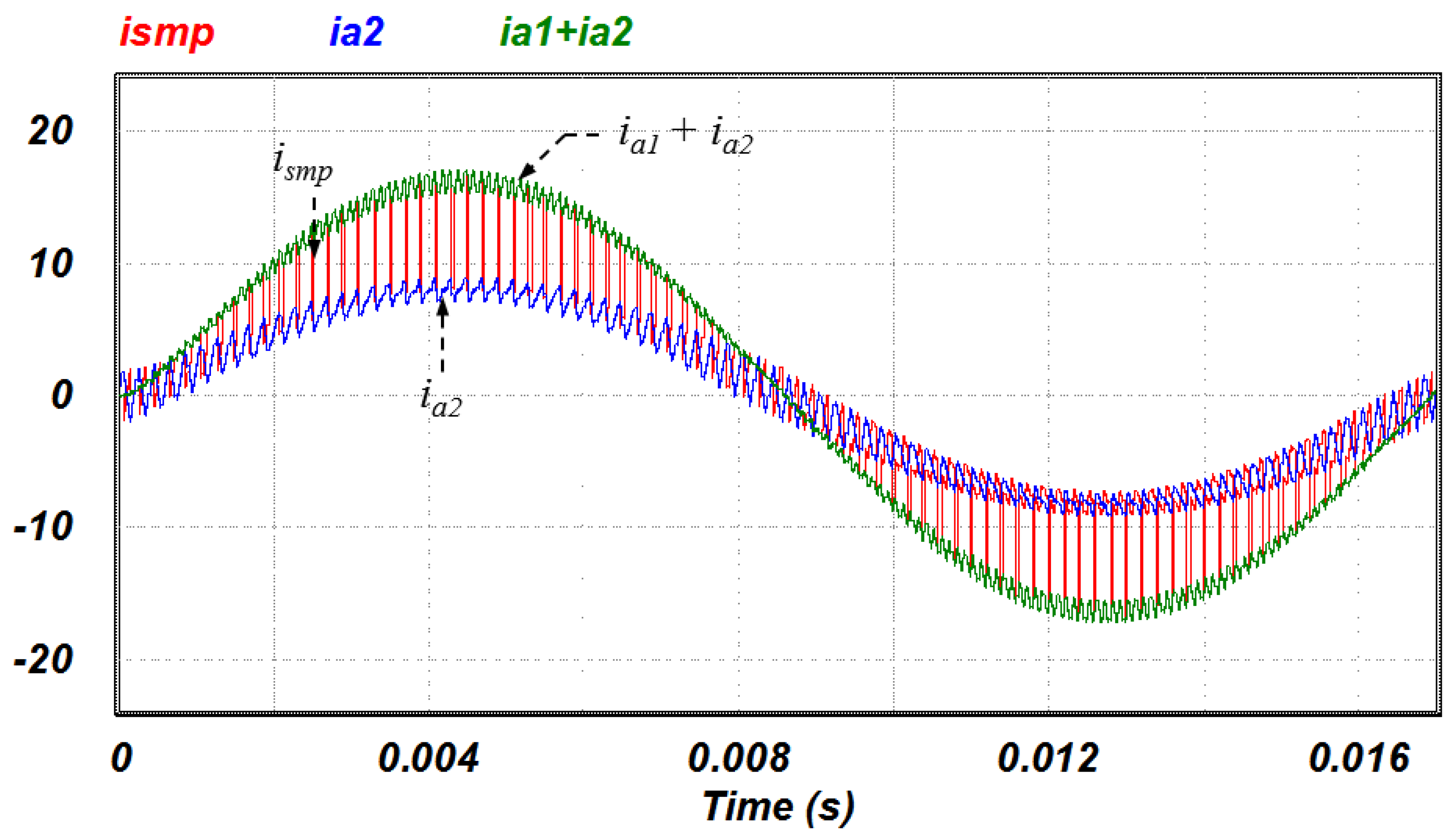
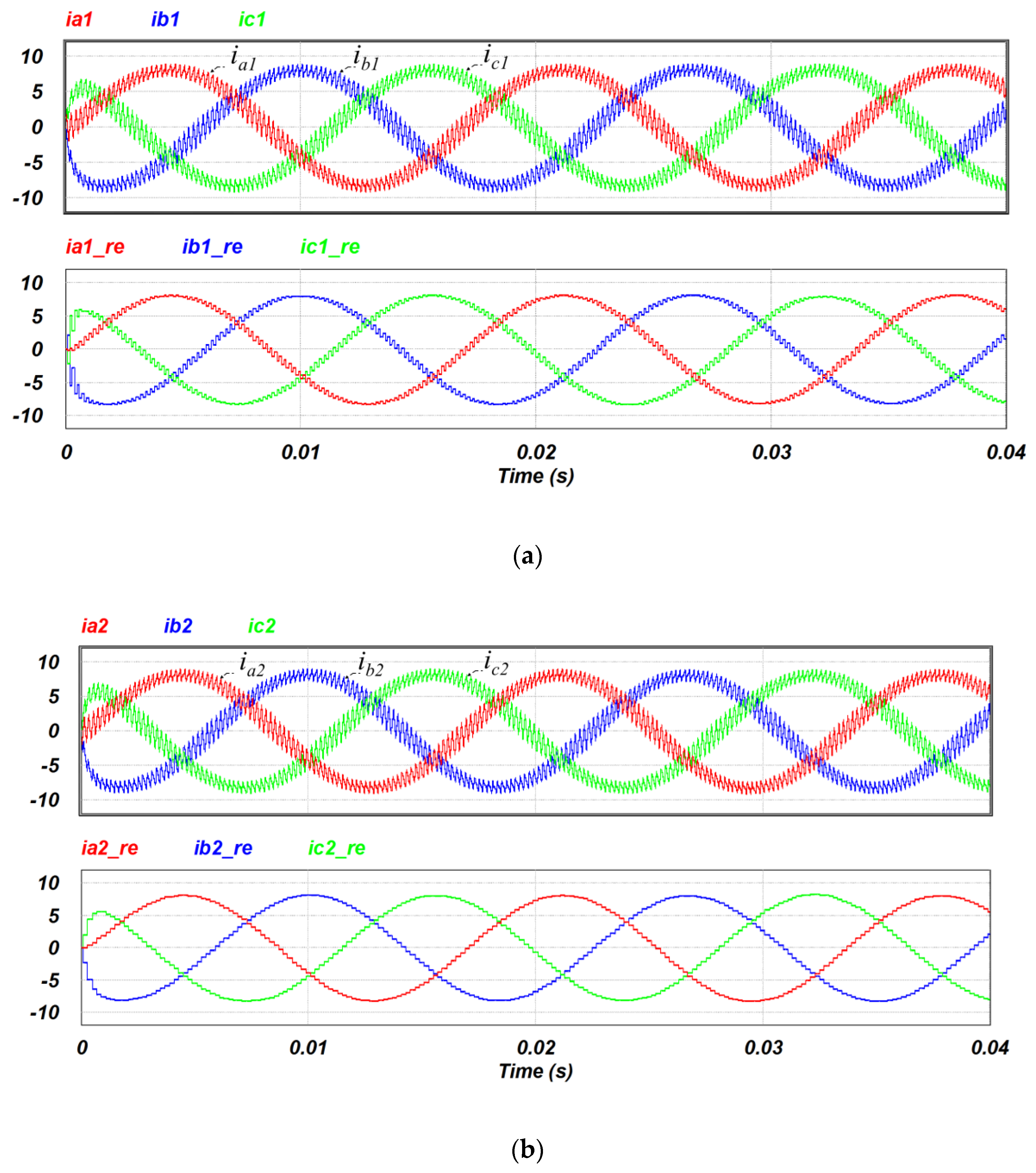
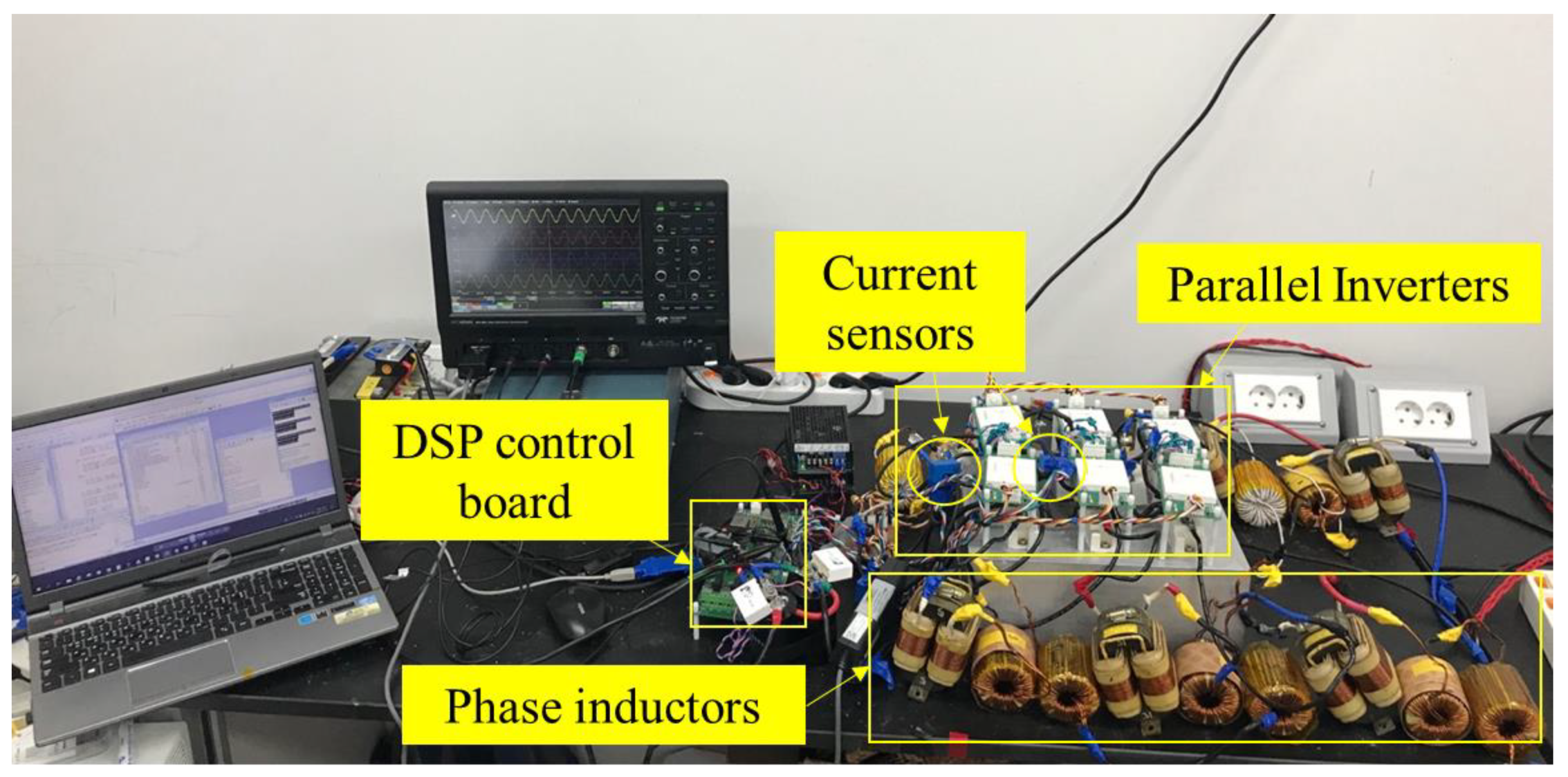
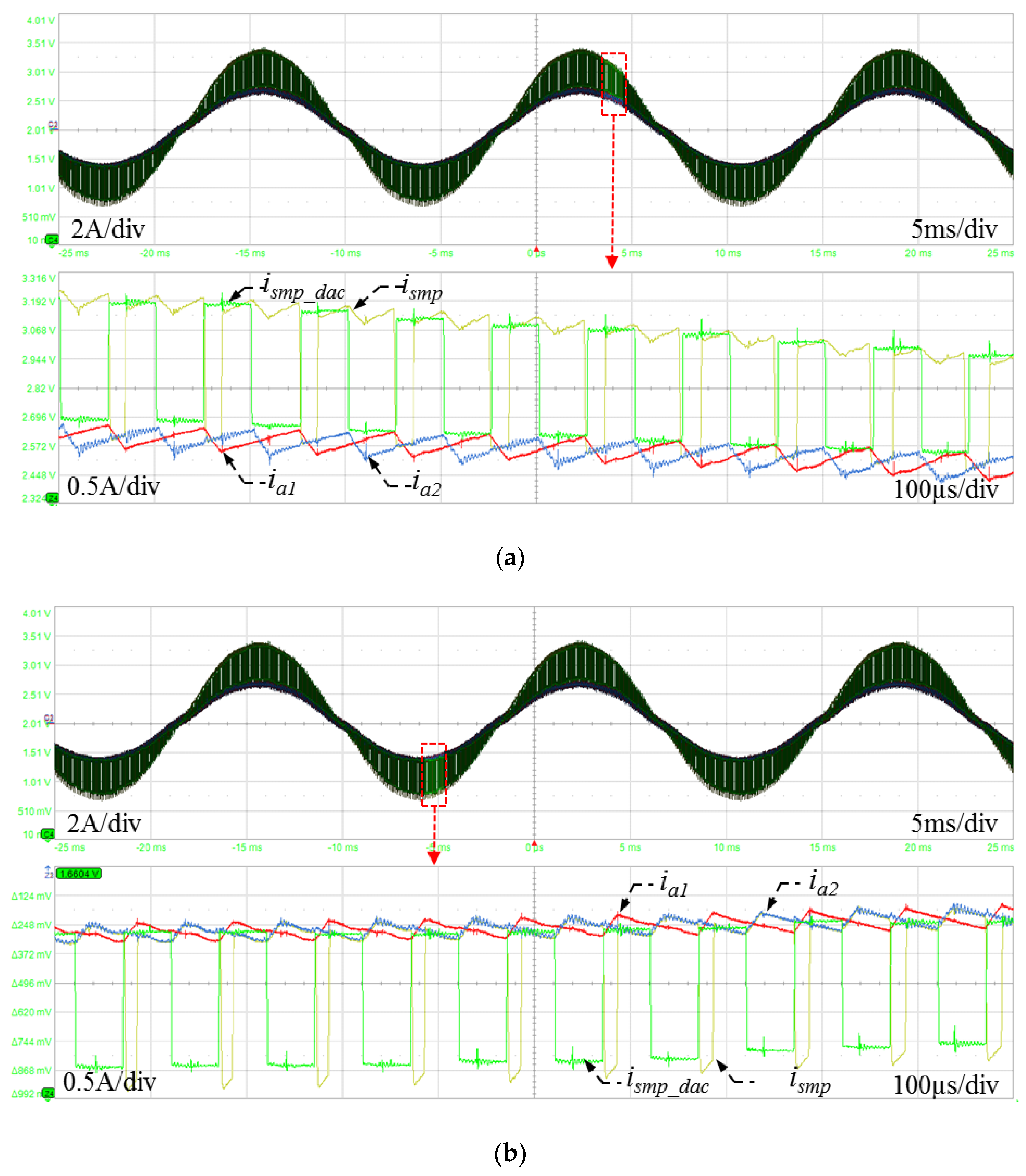
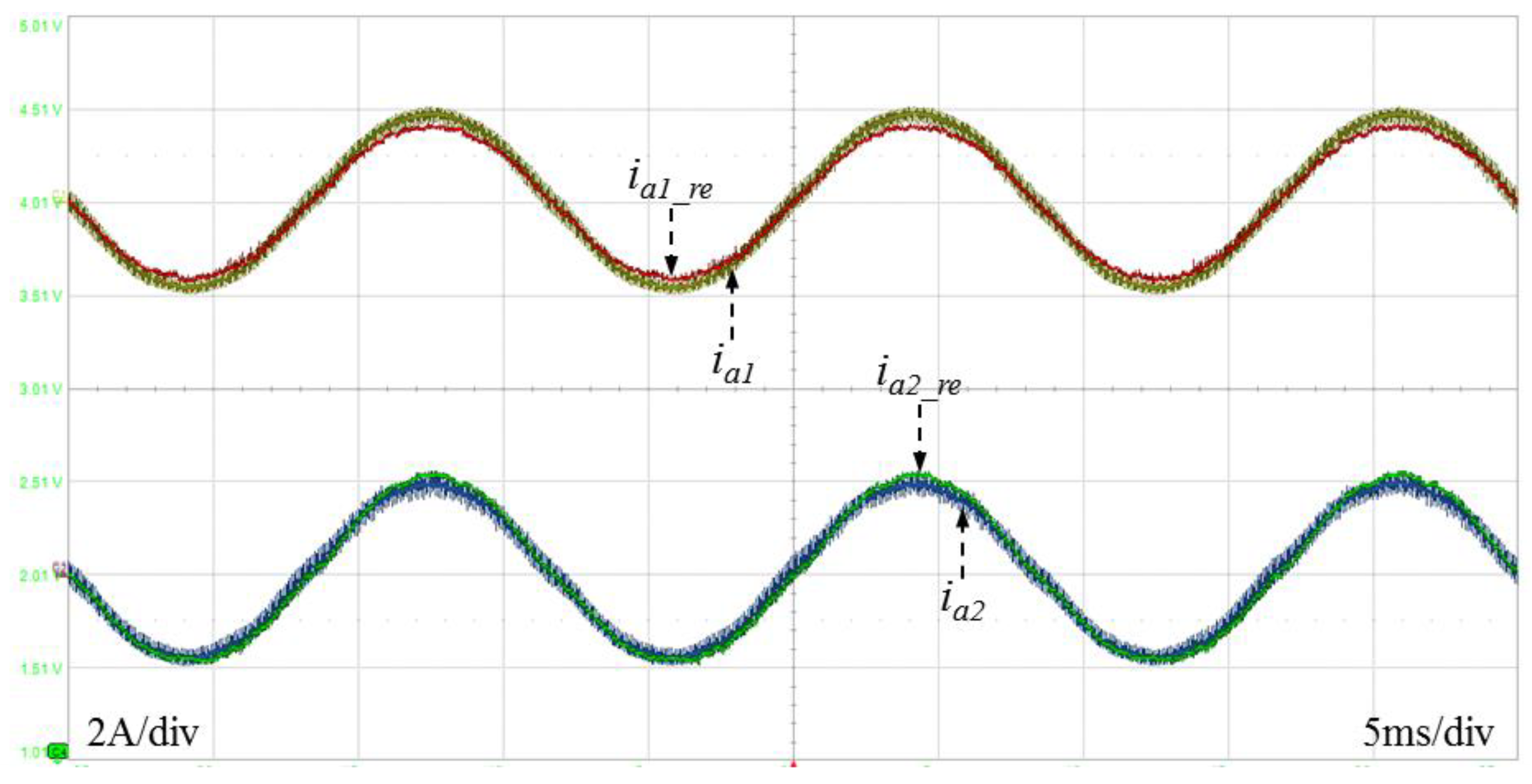
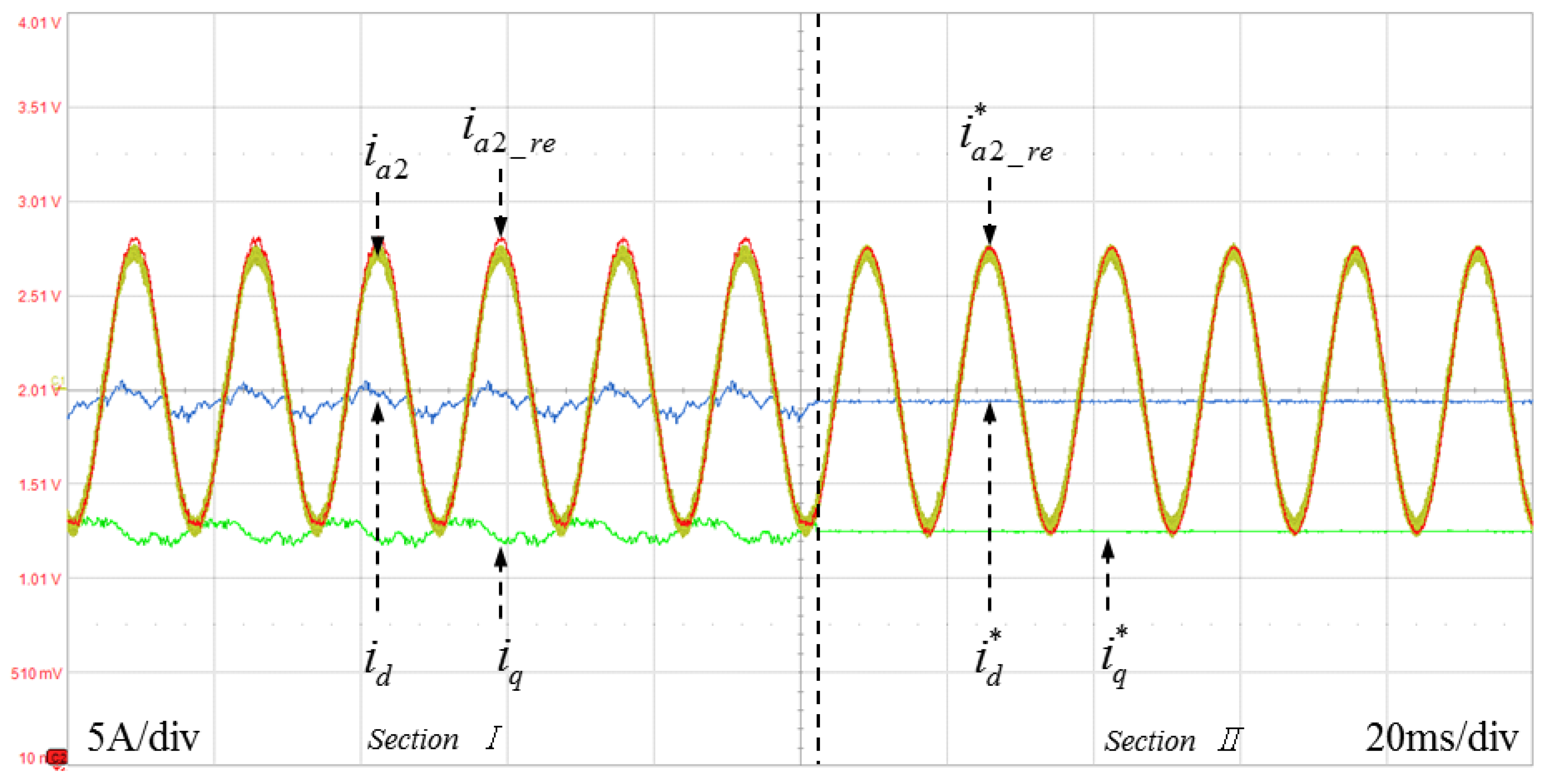
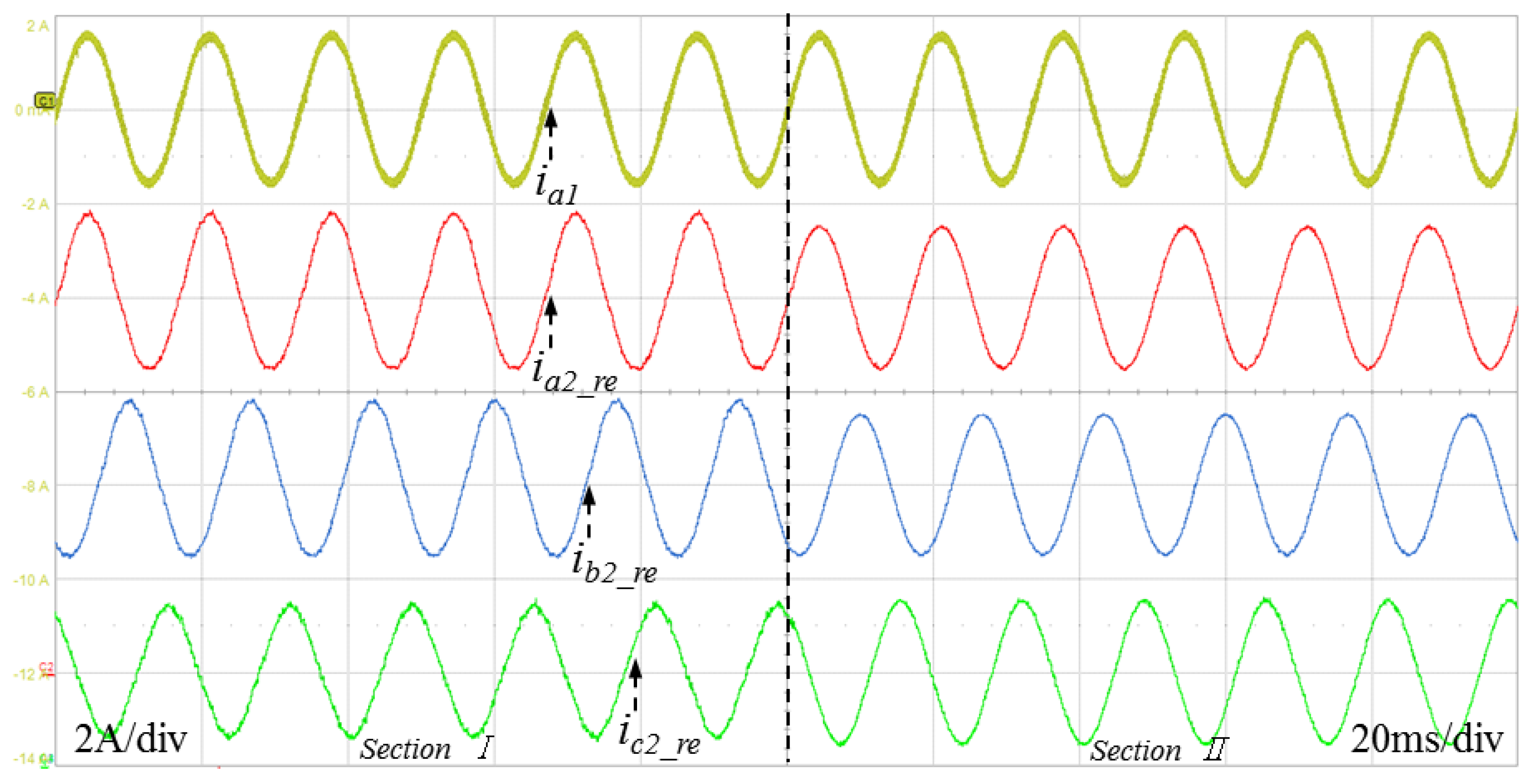
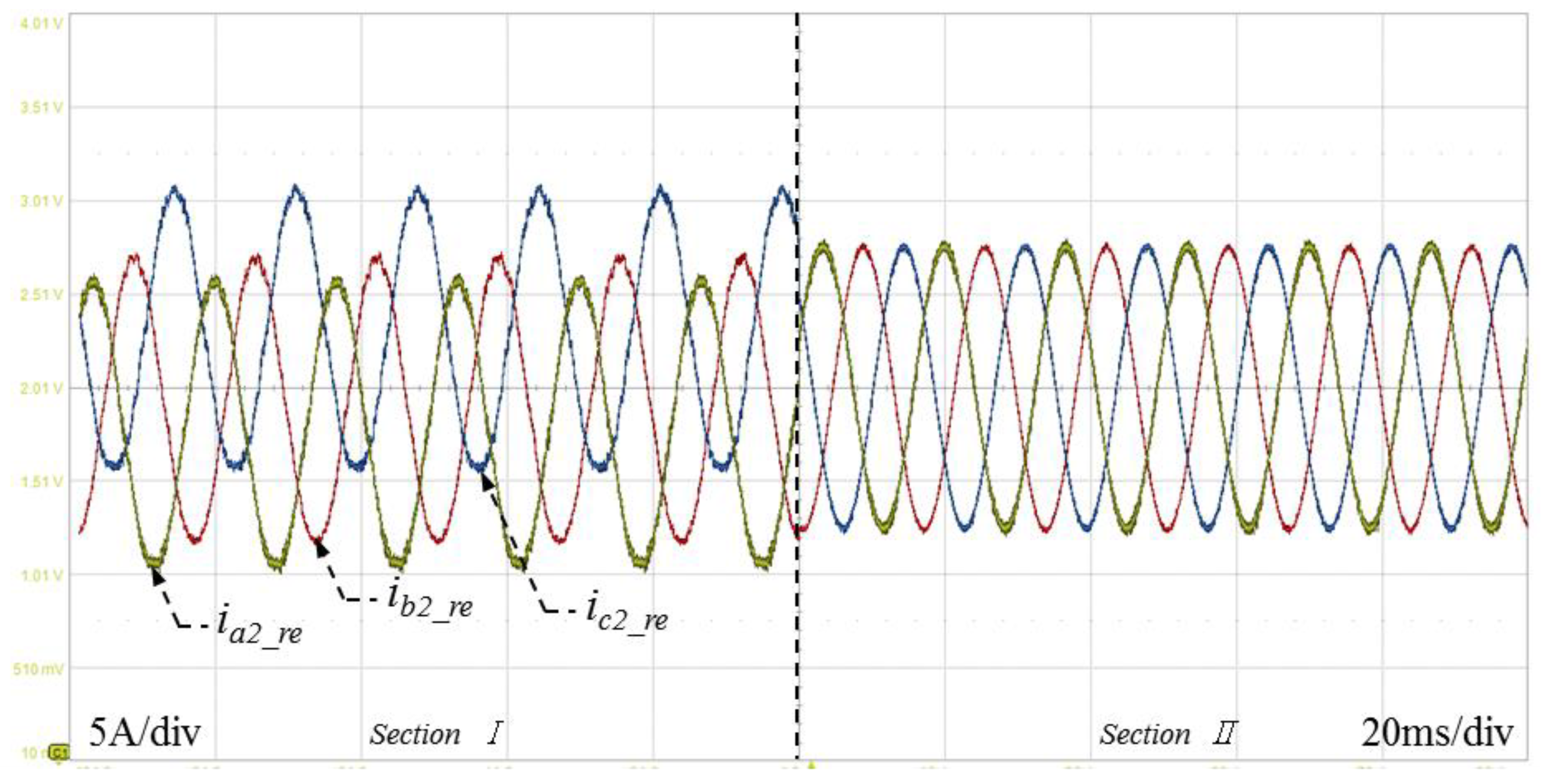
4. Experimental Results and AC Offset Compensation

Figure 6 shows a photograph of the experimental setup, and the parameters of the experiment are shown in Table 2. Two hall-effect current sensors, LA25-P (LEM, Geneva, Switzerland), are used to reconstruct each phase current of the TPPII. The power flows into the DC-link of the inverter via the DC power supply, and the TPPII is operated as an open-loop. As the each phase loads, the parallel R-C is used. The IGBT modules are used to construct the parallel inverters. A digital signal processor (DSP) control board with TMS320F28335 (Texas instruments, Dallas, TX, USA) and the external ADC configured AD7865 is used to operate the TPPII and to reconstruct the phase current. As described in Section 2, a large inductance was chosen so that the average current does not change significantly during one switching period. The switching frequency was selected to be 10 kHz higher than the audible frequency.
Figure 7 shows the actual currents ia1 and ia2 of each phase A current of the parallel inverter which sampled with current probes. Furthermore, ismp_dac is depicted; it is sampled at the proposed sampling points and converted by DAC. In Figure 7a, the waveforms of the phase A current are zoomed when the phase A current is positive. In addition, it can be seen that there is a sensing error between ismp_dac and ismp on the (0, 0, 0) vector.
On the other hand, Figure 7b shows that there is a sensing error between ismp_dac and ismp on the (1, 1, 1) vector when the phase A current is negative. These errors occur where the conduction time of the switch is small, since this paper used the bandwidth limit of the current sensor LA 25P (LEM, Geneva, Switzerland), and since the common mode noise of the ADC circuit is composed of TL084 and AD7865.
Figure 8 shows the inductor current of each of the three phase inverters and the reconstructed currents ia1_re and ia2_re using the proposed current reconstruction method. Because of the error in ismp, we can confirm that there is an error in the reconstructed currents ia1_re and ia2_re.
Furthermore, Figure 9 shows waveforms before and after the waveform applied the DC offset compensation method of inverter 2 proposed in the previous section. Section I shows the waveform without any DC offset compensation and Section II shows the waveform with a DC offset compensation. i*a2_re, i*d, and i*q are the phase, d-axis and q-axis current reconstructed by the proposed method of inverter 2.
Figure 9 shows ac ripple components in the magnitude of i*q with the proposed algorithm. When the current is transformed from the dq-synchronous reference frame to the abc reference frame, the AC ripple components which are provoked in the dq-synchronous reference frame also cause the magnitude error in the abc reference frame.
The error of i*q can be analyzed through Figure 7. If the phase current has a positive value and the voltage vector is (0, 0, 0), the output of the current sensor has the maximum error. On the other hand, when the phase current has a negative value and the voltage vector is (1, 1, 1), the output also has the maximum error. Furthermore, the errors can be assumed as AC components like Ioff_ac_P and Ioff_ac_N, because the errors vary with the fundamental frequency. Since Ioff_ac_P and Ioff_ac_N are the errors generated at same sensor, Ioff_ac_P and Ioff_ac_N have the same value as Ioff_ac. Considering the AC offset components, Equations (9) and (10) are derived as Equations (22) and (23):
( i s m p > 0 , i o f f _ a c > 0 ) i ( a , 0 ) = i a 2 + i o f f _ a c + I o f f _ d c i ( a , 1 ) = i a 1 + i a 2 + I o f f _ d c
( i s m p < 0 , i o f f _ a c < 0 ) i ( a , 0 ) = i a 2 + I o f f _ d c i ( a , 1 ) = i a 1 + i a 2 i o f f _ a c + I o f f _ d c
In Equations (22) and (23), the ioff_ac can be compensated as the condition ia1 = ia2, written as (24). i*a2_re and i*(a,0) are the equations where the DC offset compensation method is applied. ia1_re is the reconstructed current of the phase current. Furthermore, the current offset can be obtained in the same way as in Equation (27), by employing Equations (24) and (25). Thus, the compensated current in the region where the phase A current has a positive value is expressed as Equation (27):
( i s m p > 0 , i o f f _ a c > 0 ) i a 2 _ r e = i ( a , 0 ) = i a 2 + i o f f _ a c i a 1 _ r e = i ( a , 1 ) i ( a , 0 ) = i a 1 i o f f _ a c
i a 1 _ r e i a 2 _ r e = i a 1 i o f f _ a c ( i a 2 + i o f f _ a c )
i o f f _ a c = 0.5 ( i a 1 _ r e i a 2 _ r e )
i a 2 = i a 2 _ r e i o f f _ a c i a 1 = i a 1 _ r e + i o f f _ a c
Using the same principle, if the DC offset is eliminated in Equation (23) in the negative region of the phase A current, the compensated current is expressed as Equation (28), and the equation is simplified as (29):
( i s m p < 0 , i o f f _ a c < 0 ) i a 2 _ r e = i ( a , 0 ) = i a 2 + i o f f _ a c i a 1 _ r e = i ( a , 1 ) i ( a , 0 ) = i a 1 i o f f _ a c
i a 2 = i a 2 _ r e i o f f _ a c i a 1 = i a 1 _ r e + i o f f _ a c
Finally, the current without DC and AC offset is represented as Equation (30), because Equation (27) is equal to Equation (29):
i a 2 _ c o m p = i a 2 _ r e i o f f _ a c i a 1 _ c o m p = i a 1 _ r e + i o f f _ a c
As shown in Section I of Figure 10, a peak value of the reconstructed current ia1_re is smaller than a peak value of the real current ia1, and a peak value of the reconstructed current ia2_re is larger than a peak value of the real current ia2 without compensation. In Section II of Figure 10, both ia1_re and ia2_re are compensated and similar to the real currents ia1 and ia2, respectively.
In Figure 11 and Figure 12, the reconstructed phase currents of the TPPII are represented with and without proposed the offset compensation strategy.
Figure 13 shows the experimental waveform with or without the proposed strategy. In section I, artificial sensor offsets are applied at −2.5 A for the phase A current and at −1 A for the phase B current. On the other hand, in section II, when the proposed compensation strategy is applied, the DC offset of the reconstructed current is eliminated.

5. Conclusions

In this paper, a novel current reconstruction strategy using two current sensors in TPPII was proposed. The principle of the proposed strategy is described in Section 2. The simultaneously detected phase current and the branch current using a single current sensor in each inverter were used to reconstruct a three-phase current of the inverter. Furthermore, a compensation strategy for the DC offset in the reconstructed current caused by the current sensor and hardware circuit was proposed. By using Clark’s and Park’s transformation, the DC offset can be derived in a stationary reference frame and synchronous reference frame. In the synchronous reference frame, the offset in reconstructed current is simply canceled by a low pass filter. In order to confirm the effectiveness of this proposed current reconstruction strategy, both a simulation and experiment were conducted. In Section 3, the simulation results have been attached to describe the proposed current reconstruction method. Moreover, in Section 4, the reconstructed current in the proposed method is illustrated along with the actual current of TPPII. Finally, the AC offset that can occur during the experiment was analyzed and compensated online.

Author Contributions

J.K. implemented the system, and performed the experiments. Y.C. managed the paper. Y.H., S.W. and Y.W. assisted the simulation, idea development and the paper writing.

Acknowledgments

This work was supported by “Human Resources Program in Energy Technology” of the Korea Institute of Energy Technology Evaluation and Planning (KETEP), granted financial resource from the Ministry of Trade, Industry & Energy, Republic of Korea. (No. 20174030201660). This research was supported by the Human Resources Program in Energy Technology of the Korea Institute of Energy Technology Evaluation and Planning (KETEP), granted financial resource from the Ministry of Trade, Industry and Energy, Republic of Korea (No. 20174010201540).

Conflicts of Interest

The authors declare no conflict no interest.

References

  1. Qian, Q.; Xie, S.; Huang, L.; Xu, J.; Zhang, Z.; Zhang, B. Harmonic Suppression and Stability Enhancement for Parallel Multiple Grid-Connected Inverters Based on Passive Inverter Output Impedance. IEEE Trans. Ind. Electron. 2017, 64, 7587–7598. [Google Scholar] [CrossRef]
  2. Zou, X.; Du, X.; Wang, G. Modeling and stability analysis for multiple parallel grid-connected inverters system. In Proceedings of the 2018 IEEE Applied Power Electronics Conference and Exposition (APEC), San Antonio, TX, USA, 4–8 March 2018; pp. 2431–2436. [Google Scholar]
  3. Liu, Z.; Liu, J.; Hou, X.; Dou, Q.; Xue, D.; Liu, T. Output Impedance Modeling and Stability Prediction of Three-Phase Paralleled Inverters with Master–Slave Sharing Scheme Based on Terminal Characteristics of Individual Inverters. IEEE Trans. Power Electron. 2016, 31, 5306–5320. [Google Scholar] [CrossRef]
  4. Knight, A.M.; Ewanchuk, J.; Salmon, J.C. Coupled Three-Phase Inductors for Interleaved Inverter Switching. IEEE Trans. Magn. 2008, 44, 4119–4122. [Google Scholar] [CrossRef]
  5. Abusara, M.A.; Sharkh, S.M. Design and Control of a Grid-Connected Interleaved Inverter. IEEE Trans. Power Electron. 2013, 28, 748–764. [Google Scholar] [CrossRef]
  6. Hua, M.; Hu, H.; Xing, Y.; He, Z. Distributed Control for AC Motor Drive Inverters in Parallel Operation. IEEE Trans. Ind. Electron. 2011, 58, 5361–5370. [Google Scholar] [CrossRef]
  7. Green, T.C.; Williams, B.W. Derivation of motor line-current waveforms from the DC-link current of an inverter. IEE Proc. B Electr. Power Appl. 1989, 136, 196–204. [Google Scholar] [CrossRef]
  8. Ha, J. Current Prediction in Vector-Controlled PWM Inverters Using Single DC-Link Current Sensor. IEEE Trans. Ind. Electron. 2010, 57, 716–726. [Google Scholar]
  9. Lee, W.-C.; Lee, T.-K.; Hyun, D.-S. Comparison of single-sensor current control in the DC link for three-phase voltage-source PWM converters. IEEE Trans. Ind. Electron. 2001, 48, 491–505. [Google Scholar]
  10. Wolbank, T.M.; Macheiner, P.E. Current-controller with single DC link current measurement for inverter-fed AC machines based on an improved observer-structure. IEEE Trans. Power Electron. 2004, 19, 1562–1567. [Google Scholar] [CrossRef]
  11. Kim, H.; Jahns, T.M. Current Control for AC Motor Drives Using a Single DC-Link Current Sensor and Measurement Voltage Vectors. IEEE Trans. Ind. Appl. 2006, 42, 1539–1547. [Google Scholar] [CrossRef]
  12. Kim, H.; Jahns, T.M. Phase Current Reconstruction for AC Motor Drives using a DC-link Single Current Sensor and Measurement Voltage Vectors. In Proceedings of the 2005 IEEE 36th Power Electronics Specialists Conference, Recife, Brazil, 12–16 June 2005; pp. 1346–1352. [Google Scholar]
  13. Bertoluzzo, M.; Buja, G.; Menis, R. Direct torque control of an induction motor using a single current sensor. IEEE Trans. Ind. Electron. 2006, 53, 778–784. [Google Scholar] [CrossRef]
  14. Yan, H.; Xu, Y.; Zhao, W.; Zhang, H.; Gerada, C. DC Drift Error Mitigation Method for Three-Phase Current Reconstruction with Single Hall Current Sensor. IEEE Trans. Magn. 2019, 55, 1–4. [Google Scholar] [CrossRef]
  15. Shin, H.; Ha, J. Phase Current Reconstructions from DC-Link Currents in Three-Phase Three-Level PWM Inverters. IEEE Trans. Power Electron. 2014, 29, 582–593. [Google Scholar] [CrossRef]
  16. Li, X.; Dusmez, S.; Akin, B.; Rajashekara, K. A New SVPWM for the Phase Current Reconstruction of Three-Phase Three-level T-type Converters. IEEE Trans. Power Electron. 2016, 31, 2627–2637. [Google Scholar] [CrossRef]
  17. Marcetic, D.P.; Adzic, E.M. Improved three-phase current reconstruction for induction motor drives with dc-link shunt. IEEE Trans. Ind. Electron. 2010, 57, 2454–2464. [Google Scholar] [CrossRef]
  18. Cho, Y.; LaBella, T.; Lai, J. A Three-Phase Current Reconstruction Strategy with Online Current Offset Compensation Using a Single Current Sensor. IEEE Trans. Ind. Electron. 2012, 59, 2924–2933. [Google Scholar] [CrossRef]
Figure 1. Phase current measurement methods using multiple sensors or shunt resistors in 3 phase parallel inverter. (a) Current measurement with six current sensors (b) Current measurement with six shunt resistors.
Electronics 08 00179 g001
Figure 2. Current commutation path at the sampling points. (a) (Sa1, Sb1, Sc1) = (1, 1, 1). (b) (Sa1, Sb1, Sc1) = (0, 0, 0).
Electronics 08 00179 g002
Figure 3. Sampling point and proposed current reconstruction method. (a) Sampling points with PWM carriers. (b) Current reconstruction algorithm.
Electronics 08 00179 g003
Figure 4. Simulation result that shows the current sensor output with the actual currents.
Electronics 08 00179 g004
Figure 5. Simulation result. (a) The actual current and reconstructed current in inverter 1. (b) The actual current and reconstructed current in inverter 2.
Electronics 08 00179 g005
Figure 6. Photograph of the experimental setup.
Electronics 08 00179 g006
Figure 7. Experimental results. (a) The actual current and sampled current when the phase A current is positive. (b) The actual current and sampled current when the phase A current is negative.
Electronics 08 00179 g007
Figure 8. The actual current and reconstructed currents in phase A.
Electronics 08 00179 g008
Figure 9. The actual current and reconstructed currents with the synchronous current of the inverter 2.
Electronics 08 00179 g009
Figure 10. The actual current and reconstructed currents with and without the proposed offset compensation algorithm being applied.
Electronics 08 00179 g010
Figure 11. The actual current and reconstructed currents of the three phase current before and after the proposed offset compensation algorithm is applied in the inverter 1.
Electronics 08 00179 g011
Figure 12. The actual current and reconstructed currents of the three phase current before and after the proposed offset compensation algorithm is applied in the inverter 2.
Electronics 08 00179 g012
Figure 13. Experimental results before and after the proposed offset compensation algorithm is applied.
Electronics 08 00179 g013
Table 1. Simulation parameters.
ParameterValue
DC link voltage (Vdc)425 V
Phase inductor (L)5.5 mH
Switching frequency (fs)5 kHz
Dead-time2.2 μsec
Load resistor (RL)10 Ω
Table 2. Experimental parameters.
ParameterValue
DC-link voltage (Vdc)425 V
Phase inductor (L)5.5 mH
Switching frequency (fs)10 kHz
Dead-time2.2 μsec
Load resistor (RL)10 Ω
Load capacitor (CL)2 mF
Output voltage (Vout)110 V
Output frequency (f)60 Hz

