Optimum Receiver-Side Tuning Capacitance for Capacitive Wireless Power Transfer

Abstract
:1. Introduction
2. Optimum Resonant Matching Capacitor
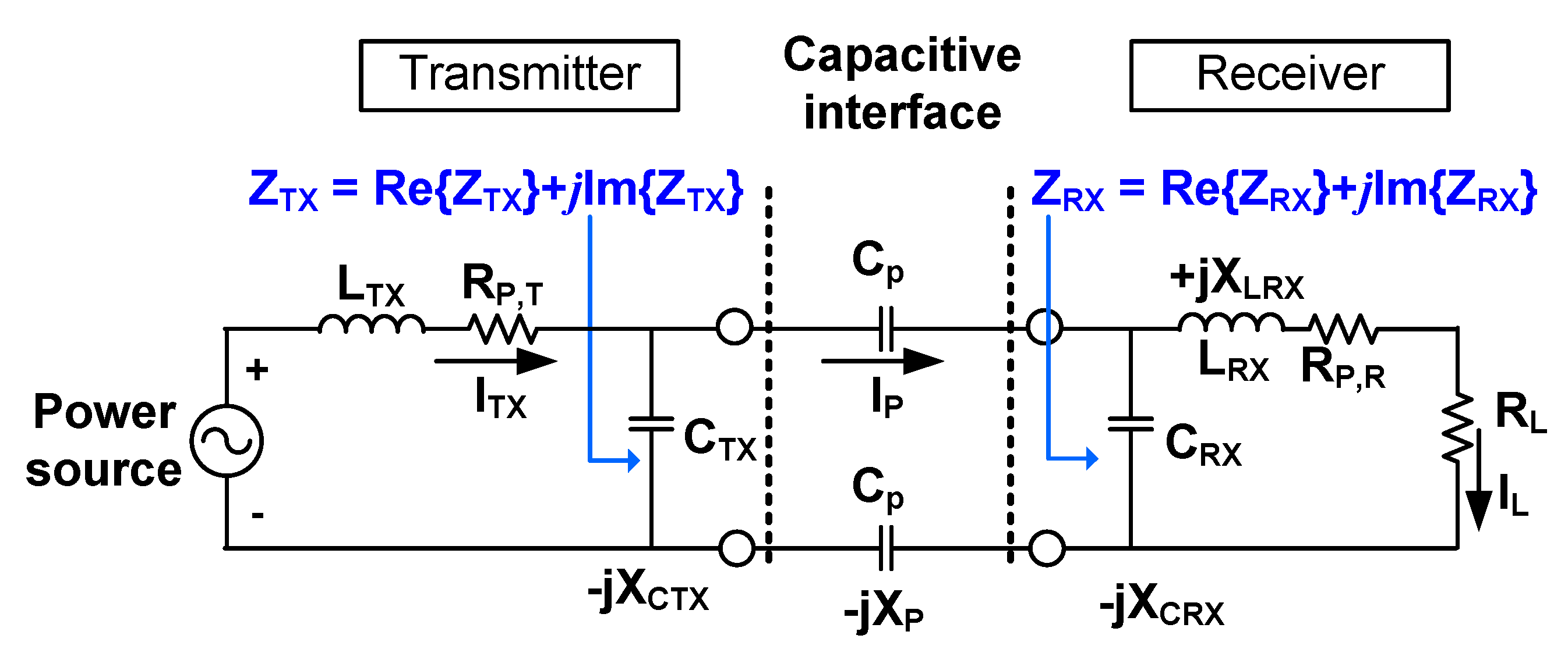
2.1. Circuit Topology of Capacitive Power System
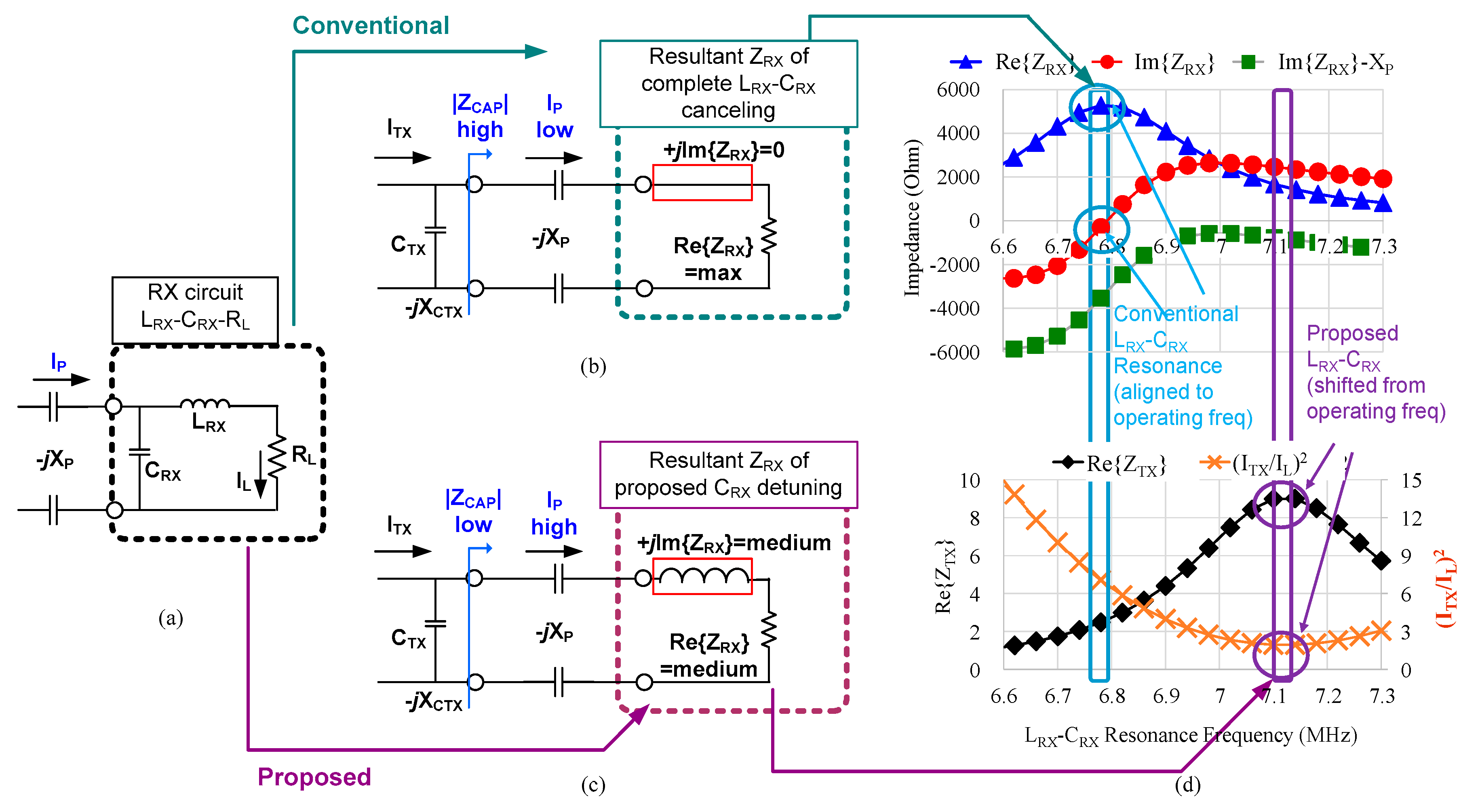
2.2. Analytical Derivation for Optimum CRX
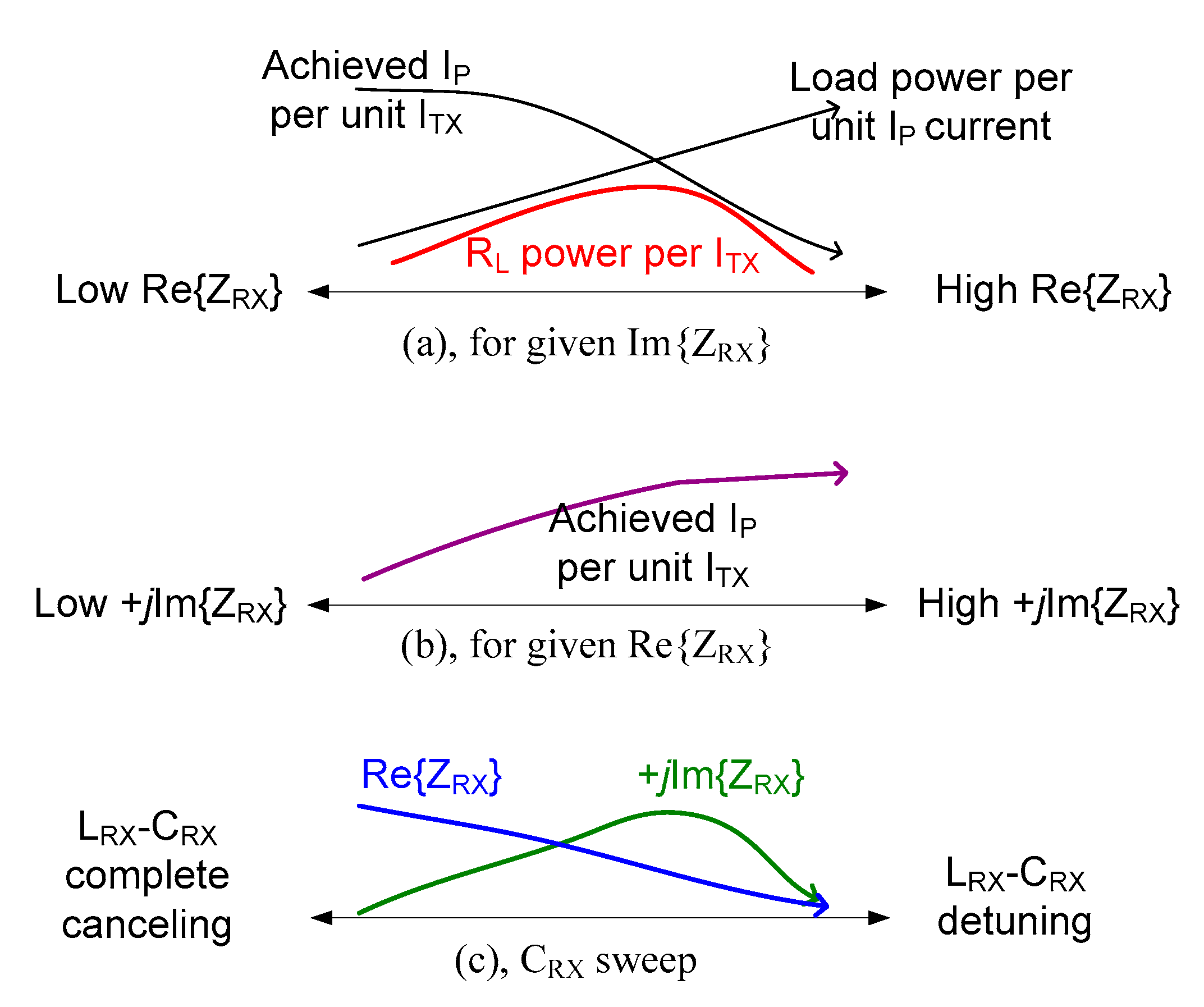
2.3. Discussion
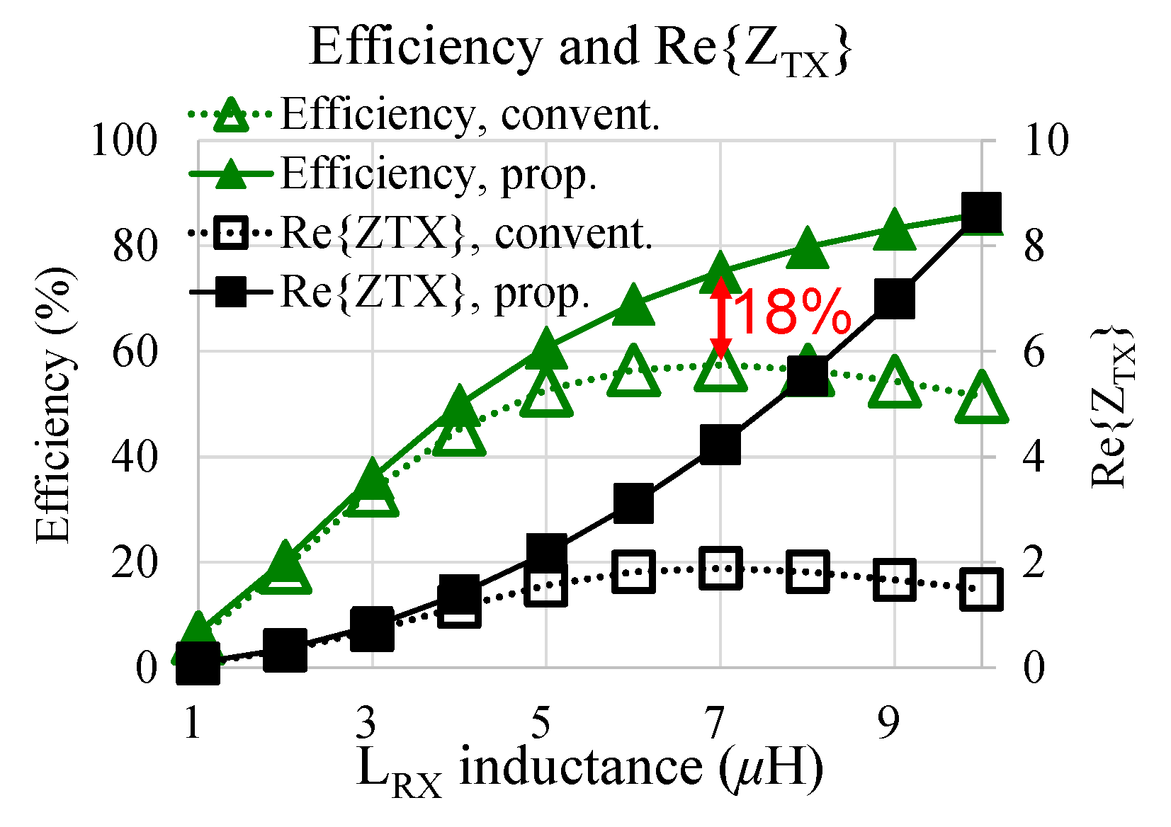
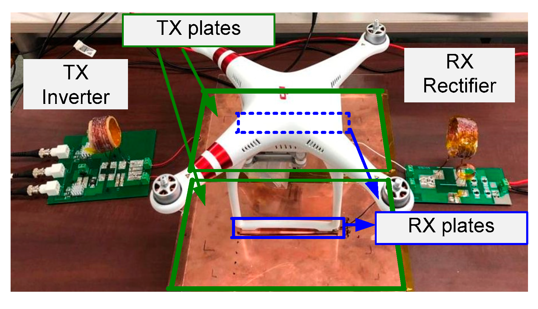
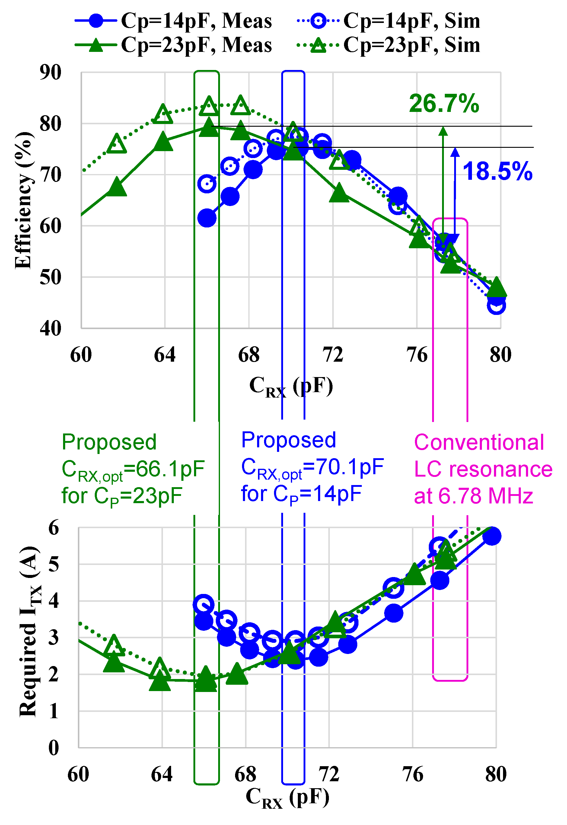
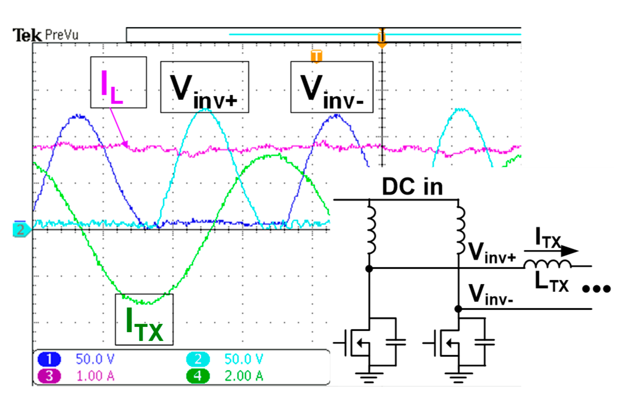
3. Results
4. Conclusions
Author Contributions
Funding
Conflicts of Interest
References
- Jegadeesan, R.; Agarwal, K.; Guo, Y.-X.; Yen, S.-C.; Thakor, N.V. Wireless power delivery to flexible subcutaneous implants using capacitive coupling. IEEE Trans. Microwave Theory Tech. 2017, 65, 280–292. [Google Scholar] [CrossRef]
- Regensburger, B.; Kumar, A.; Sinha, S.; Doubleday, K.; Pervaiz, S.; Popovic, Z.; Afridi, K. High-Performance Large Air-Gap Capacitive Wireless Power Transfer System for Electric Vehicle Charging. In Proceedings of the 2017 IEEE Transportation Electrification Conference and Expo (ITEC), Chicago, IL, USA, 26–28 June 2017; pp. 638–643. [Google Scholar]
- Lu, F.; Zhang, H.; Hofmann, H.; Mi, C. A double-sided LC compensation circuit for loosely-coupled capacitive power transfer. IEEE Trans. Power Electron. 2018, 33, 1633–1643. [Google Scholar] [CrossRef]
- Zhang, H.; Lu, F.; Hofmann, H.; Liu, W.; Mi, C. A four-plate compact capacitive coupler design and LCL-compensated topology for capacitive power transfer in electric vehicle charging application. IEEE Trans. Power Electron. 2016, 31, 8541–8551. [Google Scholar]
- Zhang, H.; Lu, F.; Hofmann, H.; Liu, W.; Mi, C. Six-plate capacitive coupler to reduce electric field emission in large air gap capacitive power transfer. IEEE Trans. Power Electron. 2017, 33, 665–675. [Google Scholar] [CrossRef]
- Dai, J.; Ludois, D. Biologically Inspired Coupling Pixilation for Position Independence in Capacitive Power Transfer Surfaces. In Proceedings of the 2015 IEEE Applied Power Electronics Conference and Exposition (APEC), Charlotte, NC, USA, 15–19 March 2015. [Google Scholar]
- Su, Y.-G.; Xie, S.-Y.; Hu, A.; Tang, C.-S.; Zhou, W.; Huang, L. A capacitive power transfer system with a mixed-resonant topology for constant-current multiple-pickup applications. IEEE Trans. Power Electron. 2017, 32, 8778–8786. [Google Scholar] [CrossRef]
- Theodoridis, M. Effective capacitive power transfer. IEEE Trans. Power Electron. 2012, 27, 4906–4913. [Google Scholar] [CrossRef]
- Zhang, H.; Lu, F. An improved design methodology of the double-sided LC-compensated CPT system considering the inductance detuning. IEEE Trans. Power Electron. 2019, 34, 11396–11406. [Google Scholar] [CrossRef]
- Li, S.; Liu, Z.; Zhao, H.; Zhu, L.; Shuai, C.; Chen, Z. Wireless power transfer by electric field resonance and its application in dynamic charging. IEEE Trans. Ind. Electron. 2016, 63, 6602–6612. [Google Scholar] [CrossRef]
- Mostafa, T.; Bui, D.; Muharam, A.; Hattori, R.; Hu, A. A Capacitive Power Transfer System with a CL Network for Improved System Performance. In Proceedings of the 2018 IEEE Wireless Power Transfer Conference (WPTC), Montreal, QC, Canada, 3–7 June 2018. [Google Scholar]


| Parameter | Value | Parameter | Value |
|---|---|---|---|
| Cp | 14~23 pF | Load | 36 V, 64.8 W |
| LTX | 3.8 μH | TX plate | 30 × 30 cm2 |
| LRX | 7.13 μH | RX pad | 13 × 1.5 cm2 |
| CTX | 165 pF | Switching freq. | 6.78 MHz |
© 2019 by the authors. Licensee MDPI, Basel, Switzerland. This article is an open access article distributed under the terms and conditions of the Creative Commons Attribution (CC BY) license (http://creativecommons.org/licenses/by/4.0/).
Share and Cite
Huh, S.; Ahn, D. Optimum Receiver-Side Tuning Capacitance for Capacitive Wireless Power Transfer. Electronics 2019, 8, 1543. https://doi.org/10.3390/electronics8121543
Huh S, Ahn D. Optimum Receiver-Side Tuning Capacitance for Capacitive Wireless Power Transfer. Electronics. 2019; 8(12):1543. https://doi.org/10.3390/electronics8121543
Chicago/Turabian StyleHuh, Sungryul, and Dukju Ahn. 2019. "Optimum Receiver-Side Tuning Capacitance for Capacitive Wireless Power Transfer" Electronics 8, no. 12: 1543. https://doi.org/10.3390/electronics8121543
APA StyleHuh, S., & Ahn, D. (2019). Optimum Receiver-Side Tuning Capacitance for Capacitive Wireless Power Transfer. Electronics, 8(12), 1543. https://doi.org/10.3390/electronics8121543