1. Introduction
Infrared photodetectors have a number of applications for both civilian and military use: night vision, medical examination, optical communications, and missile tracking [
1,
2,
3]. Over the last few years, there have been many research efforts in an attempt to develop focal-plane arrays (FPAs) capable of simultaneously imaging in two wavebands of the infrared spectrum. Some of the motivations for this research are enhanced detection capabilities of targets in sea, rain, or land clutter; the ability to distinguish between targets and decoys; and remote absolute temperature measurement that could be highly desirable in the enhancement of advanced infrared systems [
4].
Accordingly, dual-band FPAs consisting of independently readable detector pixels in each waveband within a single imaging array have obvious advantages over single-band arrays, which has led to a reduction in instrument size, weight, mechanical complexity, and power requirements [
5]. As water has strong absorption in the short-wave infrared (SWIR) waveband, the resultant water-leaving radiance approximates zero even in turbid water. Due to this property, systems that gather data in separate wavebands can effectively discriminate between both absorbing and nonabsorbing aerosols. In this manner, dual-band SWIR imaging has been critically applied in the calibration and validation of ocean-color remote sensing.
The development of these remote-sensing instruments is now entering its third generation, one being the Moderate-Resolution Imaging Spectroradiometer (MODIS) onboard Terra/Aqua satellites, acquiring data in 36 wavebands configured with three SWIR bands [
6], and the other is the Medium-Resolution Imaging Spectrometer (MERIS) onboard the Environmental Satellite (ENVISAT), providing 15 wavebands from 0.4–1.05 μm in push-broom mode [
7].
Other advanced instruments include the Global Imager (GLI) onboard the Advanced Earth-Observing Satellite II (ADEOS-II) [
8], the Geostationary Ocean Color Imager (GOCI) onboard the Communication, Ocean, and Meteorological Satellite (COMS) [
9], and the Visible-Infrared Imaging Radiometer Suite (VIIRS) onboard the Suomi National Polar-Orbiting Partnership (Suomi NPP) spacecraft [
10]. The development of these types of payloads has effectively pushed forward the adoption of multiband detection in remote sensing in space, along with other performance optimizations.
Infrared photodetector technology based on inter-sub-band absorption in III–V materials has shown remarkable success in advancing low-cost, highly uniform, high-operability, large-format FPAs [
5]. In particular, the indium gallium arsenide (InGaAs) SWIR imaging photodetector, due to its tunable bandgap, high operating temperature, and quantum efficiency, has effectively dominated the market for years. By providing a new dimension of contrast, dual-band InGaAs detection has enabled advanced atmospheric-correction sensitivity for further improvement: this advance has played an important role in the field of ocean-color remote sensing.
An In0.53GaAs0.47As epitaxial material lattice-matched to an InP substrate has a response in the wavelength of 0.9–1.7 μm, which covers three short-wave infrared atmospheric windows of 1, 1.24, and 1.64 μm, respectively. The two latter bands were considered in this article because of their stronger absorption and larger interband distance. Typically, most dual-band infrared detection systems adopt an II–VI compound semiconductor material like HgCdTe based on a quantum-well structure, which requires a high-accuracy epitaxy growth technology and an extremely low operating temperature below 180 K. Furthermore, there are but few reports in the literature of InGaAs SWIR detectors with narrow-band interference filter integration applied to a dual-band detection system, which can also work at room temperature or a relatively high temperature via thermoelectric cooler. This offers us an opportunity to meet some of the defined integration and reliability requirements for such detectors, especially in the field of space remote sensing.
This paper presents the fabrication of dual-band 800 × 2 SWIR InGaAs FPAs with interference narrow-band filters of a center wavelength of 1.24 and 1.64 μm response, designed for the purpose of broadband imaging onboard a space-remote-sensing satellite. FPA photoelectric characteristics are studied, and the infrared image of our target at room temperature thus demonstrates the detection function of the dual-band FPAs.
2. Materials and Methods
The dual-band 800 × 2 SWIR InGaAs FPAs chip had a planar structure and consisted of 2 parallel 800 × 1 linear arrays connected with an 800 × 2 readout integrated circuit (ROIC), which took into account their indium bump bonds. Circuits were designed as a readout after the integration model, with each circuit unit consisting of a capacitive-feedback transimpedance amplifier (CTIA) integrator, a sample-and-hold circuit, a shift register, and an output stage. Each pixel had a full-well capacity of around 6,640,000 e− and an input-referred read noise of 352 e−. The input offset voltage was limited to the range of ±5 mV to decrease the chance of potential dark current in our FPAs.
Furthermore, interference narrow-band filters were adapted to produce 2 channels of 1.24 and 1.64 μm, as seen in
Figure 1a. The filter was prepared using Si and SiO
2 as film material, and Al
2O
3 as substrate material. A multicavity filter structure for analyzing main peaks and a cut-off filter structure for suppression of out-of-band transmission energy were adopted. A thermoelectric cooler was used as the temperature-controlling component of our encapsulated detector module and was used to generate a high-precision temperature. A photodetector based on a backilluminated structure was fabricated on NiN-type InP/InGaAs/InP heterostructure materials using the sealed-ampoule diffusion process. A photograph of our detector chip can be seen in
Figure 1b.
As seen in
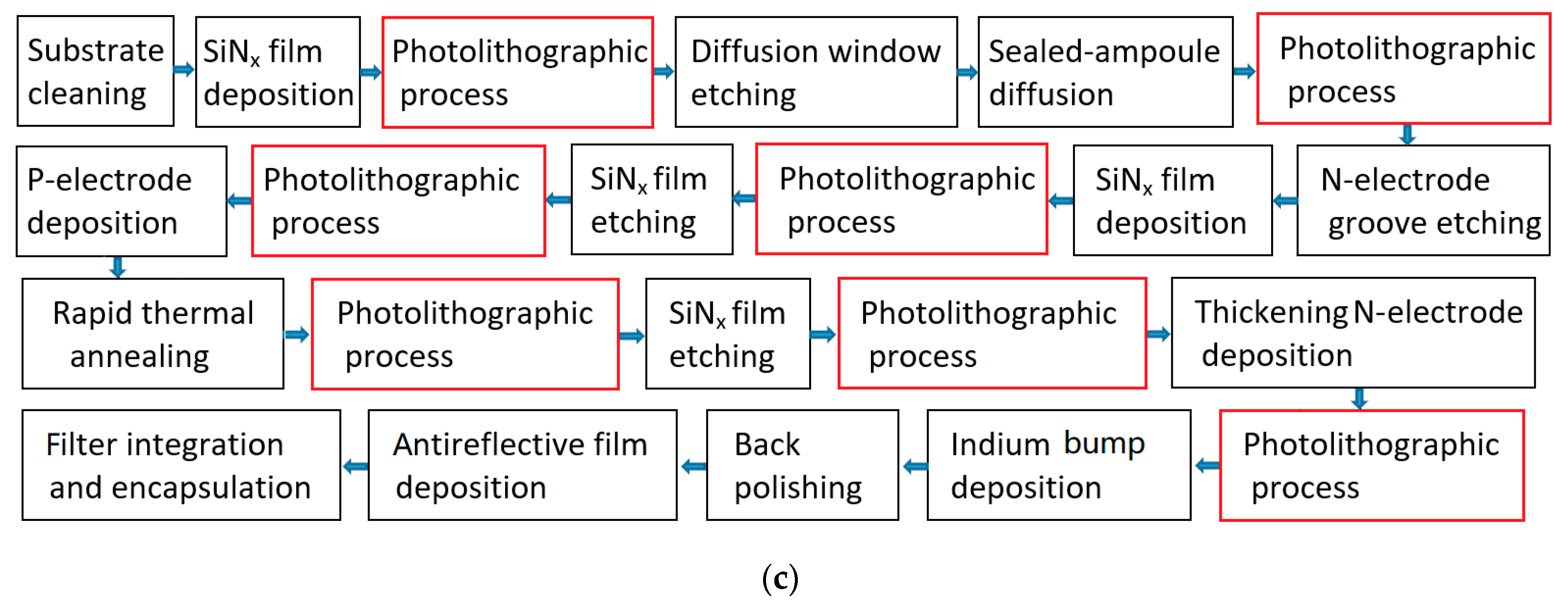
Figure 1c, the whole fabrication process of our FPAs followed a 7-step photolithography method. First, a 0.23 μm SiN
x layer was deposited onto the substrate wafer by plasma-enhanced chemical-vapor deposition (PECVD), as both a diffusion mask and for dielectric passivation. Then, the diffusion window of the photosensitive area and guard ring was fabricated using inductively-coupled plasma (ICP) etching technology, and Zn diffusion was adopted at a temperature of 803 K for 12 min to form both the P-type pixel area and guard-ring area.
Next, the N-electrode groove was fabricated with a combination of wet etching and reactive-ion etching, and a P-electrode of 500 Å Au was then deposited onto the wafer in sequence. After metallization of the P-electrode by rapid thermal annealing was complete, the n-electrode hole was dug down to the N+-InP buffer layer. Then, metal layers of 500 Å Cr/3000 Å Au that comprised our N-electrode were deposited, and the indium bump was fabricated to later connect with our ROIC. A ZnS layer was subsequently evaporated onto the polished backside of an antireflection film, and our samples were finally diced into chips and integrated with filters for assembling, packaging, and testing.
The center pixel distance of each 800 × 1 linear array was 25 μm, and the design size of each pixel was 18 × 18 μm2. The photodetector had a mirror-image relationship to the external interfaces of the two detection channel chips: a guard ring, 10 μm away from the edge pixels, was fabricated around each whole array to define its photosensitive area, which was then connected with the N-type contact via an outstretched electrode.
The spectral response of our FPAs was measured by the Fourier transform infrared spectrometer produced by Nicolet Instruments Corporation; the modulation transfer function (MTF) was studied using a laboratory system that we designed, with high precision and automation, based on the double knife-edge scanning (DKS) method. A Labsphere USS-800C uniform source consisting of a 75 W tungsten-halogen lamp and an 8 in. integrated sphere was employed to provide uniform incoherent illumination within the band of 0.9–2.5 μm. The signal and noise response were measured by an FPA measurement system using a blackbody setup as radiation source. Finally, an infrared imaging demonstration was carried out in push-broom mode.
3. Results and Discussion
From
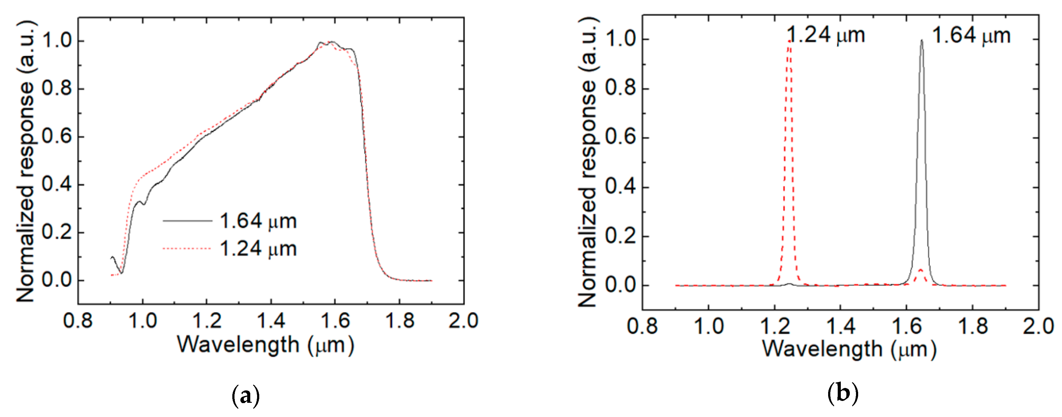
Figure 2, we can see the relative spectral response of the InGaAs FPAs carried out before and after the narrow-band filter integration at 297 K, and the spectral calibration adopted using a standard InGaAs detector. As seen in
Figure 2b, bandwidths with a 50% cutoff wavelength and response peak were 1.23–1.25 and 1.24 μm, and 1.63–1.65 and 1.64 μm, respectively. These results lined up with the designation of our filter and materials.
Weak cross-responsivity was also observed in the spectral response, which was affected by stray light after encapsulation. The edge damage to the filter caused by cutting was the most prevalent source of stray light, which resulted in a small gap when the filter was later spliced. In addition, the spectral response during filter integration was measured at 278 and 288 K, respectively, but it is not included here.
Overall, our spectral results were basically the same at different temperatures. Because the cutoff wavelength in the case of no used filter became shorter, which coincided with a drop in temperature through the energy gap of In0.53Ga0.47As, the calculated results correspondingly decreased to 1.68 and 1.69 μm, respectively; these were, however, still longer than the two compared wavebands. Therefore, the spectral curves of our FPAs with filter integration could be seen to coincide with these different temperatures.
InGaAs infrared photodetectors are mainly used for target detection and imaging. The ability to reproduce target images is one of the most important concerns in infrared applications, which is often specified by two conflicting parameters: resolution and sensitivity [
11]. Sensitivity is often described as the signal-to-noise ratio and is associated with detectivity; resolution is best characterized as the MTF [
12].
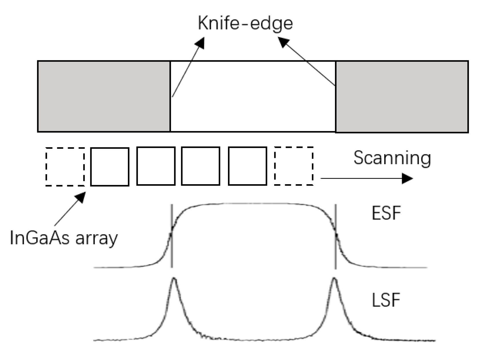
The MTF of the dual-band 800 × 2 InGaAs FPAs was evaluated on the basis of the DKS method, as seen in
Figure 3. This method was performed on the targets—two knife-edges—by each 800 × 1 linear array. By moving arrays to implement knife-edge imaging, ascending and descending diffusion function curves, which are symmetrical to each other and are called edge-spread functions (ESF), can be obtained through bright–dark conversion. Then the line-spread function (LSF) of each pixel can be generated via the discrete differentiation process of an ESF.
After Fourier transformation, the actual MTF of measured FPAs was finally estimated, given by
where F [] is the arithmetic operator of the Fourier transformation,
x is the position of the knife-edge (mm), and
f is the spatial frequency (lp/mm) [
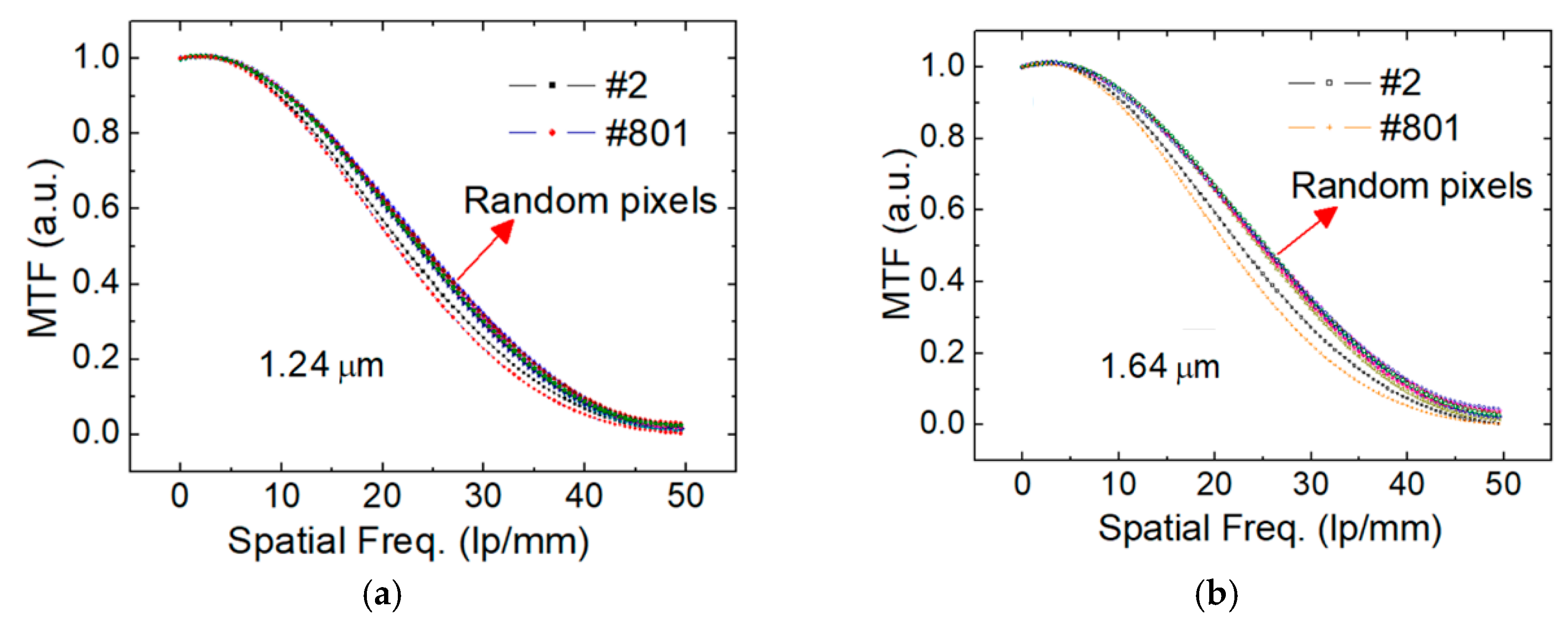
13]. The average MTF normalized at a 0 lp/mm frequency of 12 pixels (except those of #2 and #801 located at either end of the chip) and were randomly selected from two channels. Ten tests for each pixel were then carried out under similar conditions, as seen in
Figure 4.
The MTF of #2 and #801 was significantly lower than those of other middle pixels. Apart from these two pixels, the two arrays showed excellent uniformity of MTF characteristics due to the lateral collection effect of the photogenerated carriers. This resulted in outmost pixels being able to collect more carriers and achieving a larger signal under incident radiation. We further confirm this later by studying signal responsivity.
With the exception of #2 and #801, the average MTF of each pixel under test conditions in our two channels was taken as the MTF of the whole dual-band FPAs. The MTF of the two channels was very close and in the same whole spatial frequency range. Our MTF of 1.64 μm was slightly higher than that of 1.24 μm, the difference being that the largest approaching 20 lp/mm had a value of 0.033. Resolution was seen to be equal to the number of line pairs at an MTF value of 0.05 [
14].
Accordingly, the cutoff frequency of the two channels was around 43–45 lp/mm, with cutoff frequency here being the reciprocal of the pixel size in the scanning direction. This average pixel size of the two channels being estimated was calculated to be about 22.2–23.2 μm. Considering the extension of the photosensitive area in our planar InGaAs detector, the effective pixel size was close to 23 μm with a broadening value of 5 μm. Therefore, our MTF results seemed to agree with our predictions and they verified the validity of our double knife-edge scanning method.
In order to examine their optoelectronic properties, such as detectivity, pixel response nonuniformity, and pixel operability, each chip was connected through a near-infrared FPA test system under an integration time of 5 ms with a blackbody source set at 900 K. The signal and noise response diagrams of the resultant two wavebands at 297 K are as seen in
Figure 5. Each 800 × 1 waveband array consisted of 802 pixels, numbered from #1 to #802, but only a total of 800 pixels, those from #2 to #801, were actually connected to the readout circuit to generate a signal; the outmost pixels, #1 and #802, served as test pixels.
The two test pixels showed a larger signal response than that of internal pixels marked with red rectangles in
Figure 5, which could have easily behaved like blind pixels due to the excessive signal response. For our InGaAs photodetector with a planar junction structure, there was no physical separation between neighboring pixels. As a result, some of the electron–hole pairs generated in pixel #1 would be collected by the adjacent pixel (#2) due to the lateral collection effect of photogenerated carriers. Normally, if the relevant properties of #1 and #2 were read out at the same time, there would be a competitive relationship between them to collect carriers, eventually reaching a balance. However, #2 would absorb more carriers than those generated in #1, although this may not be easily observed under test conditions.
Therefore, the lateral collection effect of photogenerated carriers contributed to the larger signal output of #2 as compared to the signal output of other internal pixels like #3, which was about 1.2 and 1.0 V, respectively. Similarly, this phenomenon also arose between #801 and #802, which would also cause obvious MTF attenuation. In order to address this problem, pixels at both ends of each 800 × 1 array were short-connected to an N-type electrode, analogous to a guard ring, with most of the carriers generated in #1 and #802 unable to be collected by #2 and #801.
Due to this design, our problem of excessive signal response was solved, and the signal response of #2 and #801 returned to normal. The mean signal and noise of the 1.24 channel μm were 0.90 V and 121.66 μV, and those of the 1.64 channel μm were 0.94 V and 122.06 μV, respectively. Additionally, the pixel operability of each 800 × 1 near array was close to 100% after suppression of this excessive signal.
Nonuniformity of infrared FPAs is a critical factor that affects the detection range of infrared imaging systems, especially those used to detect small and dimly lit objects [
15]. Nonuniformity of InGaAs infrared detectors is related to the epitaxial materials involved and the fabrication process, which has several causes: the nonuniformity of the photosensitive area, circuit (e.g., capacitance, gain, bias voltage), blackbody source, and surface passivation. Response nonuniformity
showed that the pixels of the FPAs retained slightly different photoelectric properties, and it is given by
where
and
are the signal response and its mean value, and
the number of pixels. The calculated results reached ideal values of 2.48% and 2.61% of a 1.24 and 1.64 μm waveband, respectively. Peak detectivity
of the FPAs was described as
where
and
are the factor and blackbody detectivity, respectively [
16]. The
for both was 77.0, calculated from the spectral response when blackbody temperature was at 900 K. After the temperature was lowered to 278 K via thermoelectric cooler, mean peak detectivity was 4.39 × 10
12 and 5.82 × 10
12 cm·Hz
1/2/W, quantum efficiency was 90.13% and 87.89%, and responsivity was 0.90 and 1.16 A/W, respectively. Moreover, the average density of dark current at 295 K was 6.94 and 9.42 nA/cm
2 (@ 10 mV), respectively, with only slight zero drift.
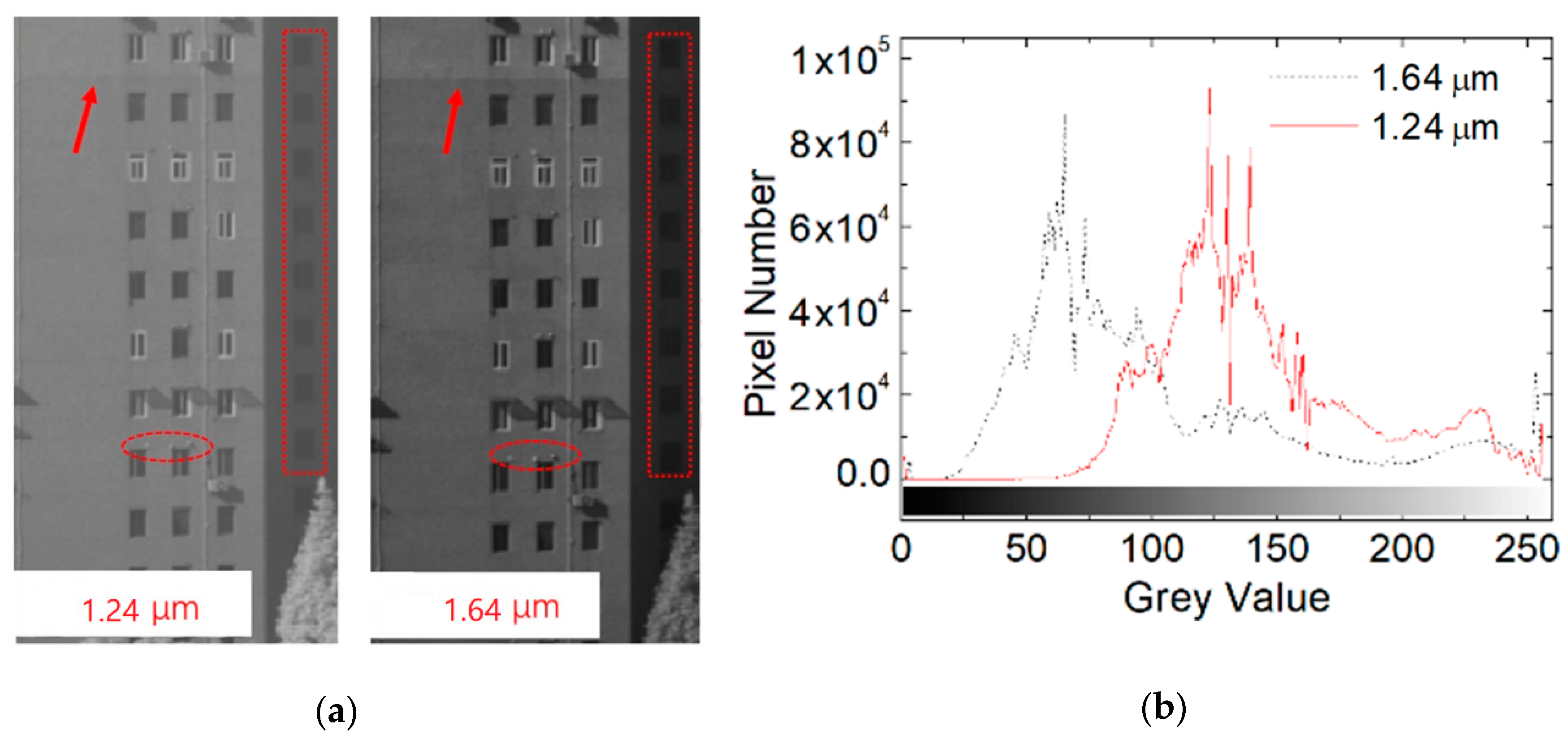
In this work, the effectiveness and feasibility of dual-band InGaAs FPAs were validated through an infrared imaging experiment in push-broom mode performed via a high-precision turntable placed outdoors on a cloudy day without sunlight. The excellent infrared detection imaging from each channel can be seen in
Figure 6. Note that the boundary and raised objects of exterior walls, indicated by the red arrow and elliptical circle, were relatively clearly imaged at 1.64 μm, while the windows were easier to observe at 1.24 μm.
Distinctions can be drawn from the gray-value distribution shown in
Figure 6b. These results indicated that the pixel-intensity distribution of 1.64 μm was skewed more to the darker side when compared to that of 1.24 μm. Moreover, the variance span of the whole range of 1.24 μm was relatively wide, indicating that the image had remained relatively clear. Because the response information of long-waveband infrared mainly comes from the thermal radiation of the target, our 1.64 μm channel had the characteristics of an obvious hierarchy, as well as a sensitive response at a lower target temperature. Conversely, the shorter waveband photodetector could provide more information about light scattering and reflection. We could therefore see that a strong response occurred at higher pixel intensities in bright regions with large grey values in the corresponding image, and especially at higher temperatures; this can be seen in
Figure 6a.

