1. Introduction
Programmable logic controllers (PLCs) were originally designed as industrial digital computers for high reliability control and ease of programming. Currently, they have been widely adopted for different environments, including home automation systems. The internal architecture of a PLC determines its optimal programming language. For this reason, most PLC manufacturers offer their own programming languages that can be naturally translated to the controller’s machine code and optimally utilize its hardware resources. IEC 61131-3 standard [
1] is an attempt to standardize and systematize programming languages for PLCs. Many deficiencies of this specification have been discussed in the literature; e.g., in [
2,
3]. Even though some PLC manufacturers offer controllers that can be programmed using languages that conform fully, or almost fully, to the IEC 61131-3 standard [
4,
5,
6,
7,
8], the internal languages or construction of the CPUs of the PLCs have instruction sets that are not compatible or are only partially compatible with it.
Often, regular microprocessors are used as the processing units of PLCs featuring standard language compatibility. In such cases, the IEC languages are implemented in a multiple-level translation procedure utilizing substitution of standard language instructions by subprograms or sequences of statements given in the C/C++ language. This approach introduces indirect implementation that is far from optimal due to its general nature [
9,
10,
11]. The same applies to bit-byte (bit-word) units. The control program can be decomposed for bit and byte/word calculations [
12]. In many cases, these parts can be executed concurrently. However, these parts interact with each other, and the CPU must be equipped with an exchange or synchronization block [
13].
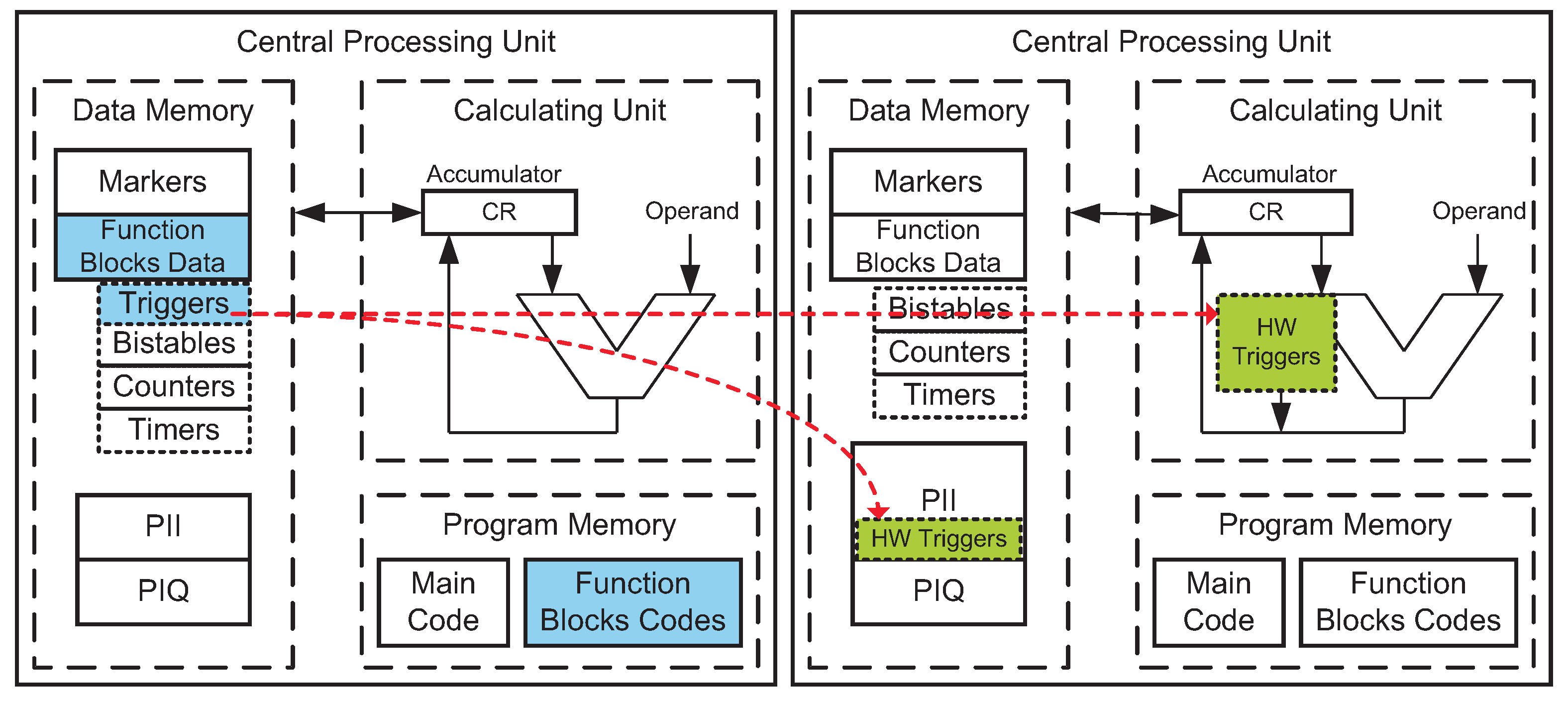
One of the most frequently used functionalities in PLCs is the edge detector, which is used for external signals, internal function triggering, etc. The classical approach to this problem is that the trigger function is processed in using software. The processed data are stored in data memory, and the software procedures for the trigger function are stored in function block codes located in program memory. The trigger task consists of creating the proper data structure in data memory and executing the procedure. Two main disadvantages can be encountered: it is necessary to have memory for the data structures and function codes and spend CPU time for processing the procedure of the function block for each bit, which takes several clock cycles. The classical structure is presented in
Figure 1 (left side).
A custom CPU can be designed and tested using hardware description languages. It can be implemented in an FPGA structure utilizing synthesis tools [
8,
14,
15]. This is a serious facility for vendors that design and manufacture PLCs. This paper focuses on a hardware implementation of edge detection function blocks (EDBs) (
Figure 1 (right side)), which are one of the basic types of blocks in typical PLC applications. The general idea of an EDB defined in IEC Standard 61131-3 [
1] is presented, and the possibility of its implementation (including an FPGA-based system-on-a-chip) is shown.
2. Trigger Function Background
Trigger functions are functional operators that are very simple, very useful and often used. The algorithm for triggering the state of the variable is quite simple (Listing 1): the variable is loaded into the current result register CR (called Accumulator) <1>; the simple logic function on the CR and the previous state of the variable (located in memory) are carried out <2> and copied to output <3>; and then the present state of the variable is copied into memory for the next usage <5> of the trigger function. As the effect of a logic function, the current state of the variable is destroyed, and thus, it must be restored in the CR <4>.
| Listing 1. The pseudo-code for trigger operators. |
- 1
IN->CR - 2
CR and not MEM -> CR - 3
CR->Q - 4
IN->CR - 5
CR->MEM
|
Another solution can be proposed; i.e., to build the shadow CR register, CR’, into the processing unit. However, two different methods of shadowing can be implemented: one in which the input data loaded into the CR are always shadowed—Listing 2: left side <1> or one in which the CR is shadowed only for a particular function; e.g., when triggering begins—Listing 2: right side <2>.
| Listing 2. Trigger function with additional current result (CR’) memory bit: two versions. |
 |
The standard does not specify exactly how the “remembering” is to be achieved or whether or not the cell is to be freely accessible to the programmer. Trigger functions have been achieved in different ways for different PLCs. For example, Siemens’ PLCs use two methods:
Explicit, in the family S7-300/400 and S7-1200/1500 where standard memory elements are used for the edge detectors; these are often memory elements, M (called markers), or cell data blocks, DB [
16];
Implicit, in the S7-200 controllers where the programmer does not see the edge detector memory element; the memory element is attached automatically in the assembly phase of the program; the programmer does not have access to it [
17].
A third way used is the Concept PLCs made by Schneider. The programmer sees that the operator has assigned a memory element. However, it is not available directly to the programmer. It is simply the name of the copy of the function block (instance name) [
18].
Another nuance that must be considered is whether or not the variable used as a memory marker for the trigger function is retentive. In other words, it is important whether it is remembered or cleared when the PLC is switched in a sequence RUN→STOP→RUN. This is very important, as it determines the behavior of the edge detector after restarting the PLC.
Figure 2 and
Figure 3 show the behavior of a few selected PLCs in such situations.
As can be seen in
Figure 2, both the Siemens S7-300 and the Schneider CONCEPT, at least in one case, behave as if there were a rising edge. The trigger function in the Siemens S7-200 does not generate a pulse for a rising edge detection either in the programming language STL-Siemens or the STL-IEC. The rising edge trigger function implemented according to the IEC61131-3 standard will behave the same as the Siemens S7-300.
Unlike for the case of a rising edge, the Siemens S7-300 falling edge function behaves contrary to the IEC61131 norm in the case of non-retentive markers (
Figure 3) because these markers are cleared, so edges that arise in the STOP mode are not considered falling edges after a STOP to RUN sequence of the PLC. Non-retentive markers used for falling-edge trigger functions ought to be set to work according to the IEC61131 standard. Two other PLCs, the Siemens S7-200 and the Schneider CONCEPT, work the same as in the case of rising edges.
In the authors’ opinion, the trigger function should respond only in the case where the change has been reported in two consecutive loop cycles in running the PLC. The edge that arises during a STOP mode should not cause edge detection. In general, it is safe for the end user. Taking into account the safety, it should be noted that the behavior of the Siemens S7-200 PLC is correct from this point of view. Unfortunately, the behavior of the trigger function proposed in the IEC 61131-3 standard is unsafe. The Siemens S7-1200 PLC works the same as the S7-300 for rising and falling edges [
19,
20].
3. Hardware Implementation of Trigger Functions
The most important problem in the classic edge detectors presented in
Section 2 is the time it takes to execute this function. Hardware implementation of trigger functions may be built more efficiently than software functions in terms of time and resources. The trigger function can be implemented by means of a flip-flop and a logic gate. The result must be saved in a second flip-flop. In fact, it is possible to implement two hardware-based variants of trigger functions: “safe” and IEC61131. To compare both solutions, simplified figures of the rising edge trigger function implementations are presented in
Figure 4 together with the waveforms. Questionable points are marked in red on the waveforms. Waveforms marked with an asterisk represent behavior for retentive memory. The usage of retentive markers (flip-flops) is not good when safety needs to be taken into account.
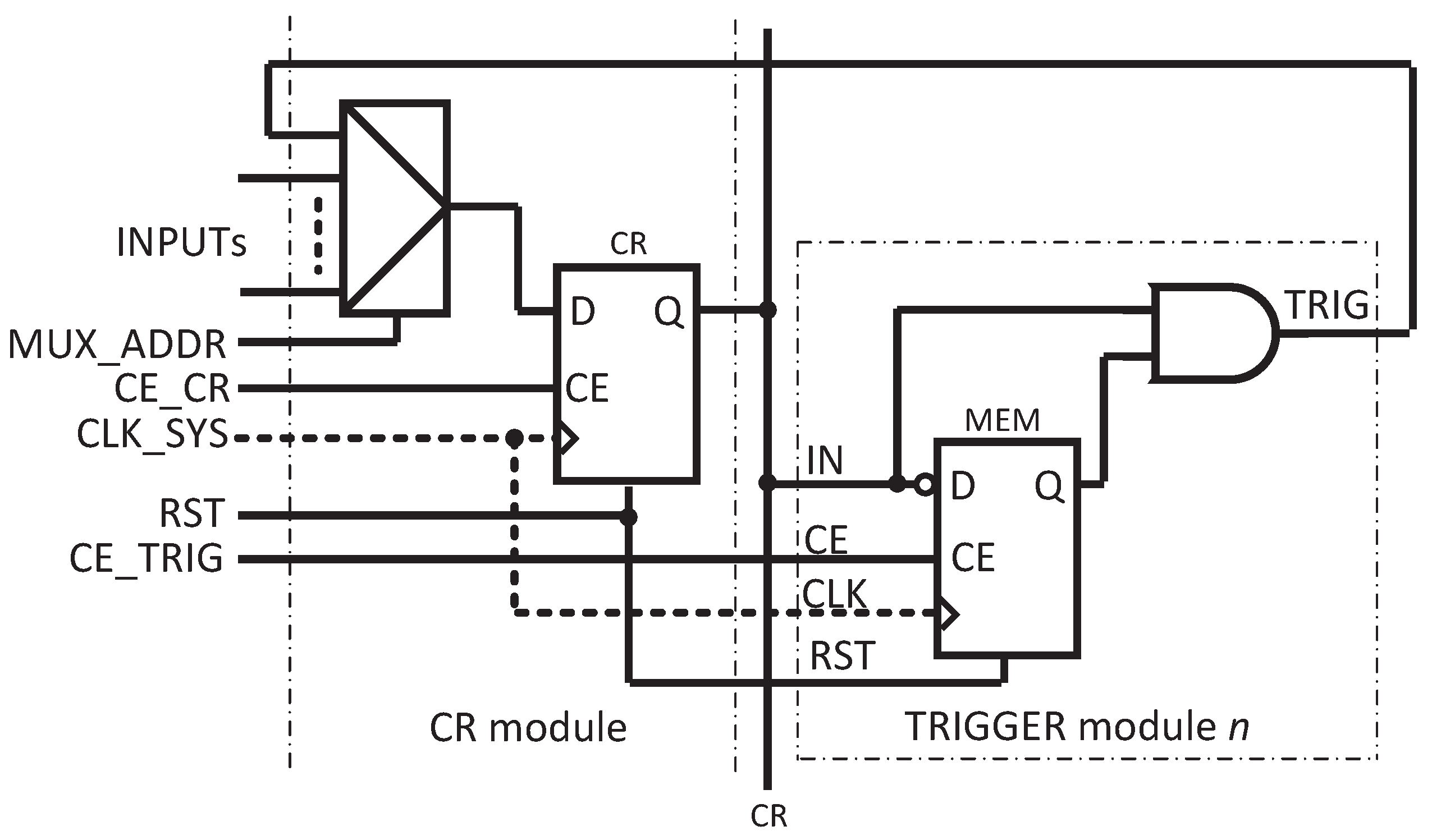
The proposal for a rising edge trigger module included in a CPU is presented in
Figure 5. There is no necessity to make an extra copy of the CR because it is rewritten to the MEM flip-flop at the same time, as the result of the trigger function is written to the CR. Of course, the CR module multiplexer must be opened for trigger feedback. There are three other control signals generated by the CPU. First, the flip-flops are triggered by means of a CLK_SYS signal. However, the particular module (CR, TRIGGER, etc.) must be enabled at a particular time for the particular instruction. It is possible to use the clock enable (CE) input of the flip-flop and control the capture of the data into the D flip-flop. These are CE_CR for the CR module and CE_TRIG for the TRIGGER module. The structure presented in the
Figure 5 uses the technique for proper clock gating with flip-flop CE input [
21]. Such a technique requires only one clock domain and eliminates SKEW or metastability.
A synthesizable Verilog model of a hardware implementation of the rising edge trigger (TRIGGER module
n for
Figure 5) is presented in Listing 3. In fact, the CR module is part of the CPU. However, it was necessary to model it for simulation purposes.
| Listing 3. Hardware implementation of trigger functions (Verilog model). |
 |
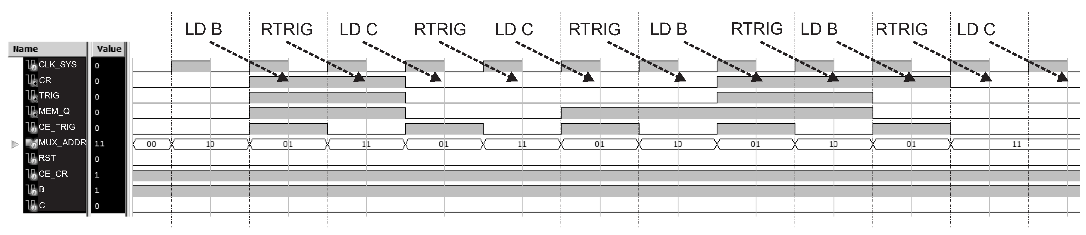
To check proposed designs, a simulation of the structure presented in
Figure 5 has been executed. The simulation time diagram is presented in
Figure 6. To simplify the simulations and their analyses, CE_CR was set to “H”, so the CR module was always active. The RST signal is inactive. Inputs B and C are constant and are set to “H” and “L”. It is not necessary to show the MEM_OUT signal; however, showing it is helpful for the analysis.
The trigger block implemented in the CPU structure must be fully configured. There must be two special register bits: DIR and CTRL. The first bit (DIR) is responsible for choosing the edge: 0-rising, 1-falling, while the second bit (CTRL) corresponds to the behavior of the module: 0-SAFETY or 1-IEC-based (
Figure 7). The DIR control bit should be part of a special function register, or the element of the data structure for edge detection, because a programmer may change this bit for particular trigger blocks. The CTRL control bit can be only one for the whole CPU because the decision about trigger block functionality, in general, is only made once at the initialization stage. The clock path of the trigger block presented in
Figure 7 can be changed to the structure with clock enabled input (CE), as presented in
Figure 5.
Edge-triggering blocks may be used as implementations of trigger function used explicitly (as function block) or implicitly (e.g., as edge-triggered input for count inputs in counters).
4. Input with Automatic Edge Detection
The input variable in IEC 61131-3 can be declared with an attribute. The standard provides R_EDGE and F_EDGE for rising and falling edge detection (Listing 4).
| Listing 4. Declarations of edge inputs. |
VAR_INPUT X: BOOL R_EDGE;
y: BOOL F_EDGE;
END_VAR |
The examples and explanations presented in the standard [
1] and in related literature, e.g., [
22], show that the trigger function is executed for each input in a classical manner. According to the standard, this will cause the implicit declaration of the edge-detection function to perform the required edge detection. In another words, the input must be loaded into the CR, and then the trigger function is applied in order to "detect" the edge. It takes time for edge triggering of every declared as R_EDGE/F_EDGE input one by one, so there is no advantage of the R_EDGE and F_EDGE attribute.
Another structure can be proposed. Let us build in the hardware edge detector on every input and use either the state of the input (classical PII image) or the trigger value of the input [
23]. In this case, the programmer may use the state of the input or directly use the edge value. The structure is proposed in
Figure 8.
The main advantage of this solution is that the edge of every input with an R_EDGE and F_EDGE attribute is detected at the beginning of the control loop simultaneously. This takes only one system clock period.
One more optimization can be performed. The MEM flip-flop presented in
Figure 8 is used to remember the state of the input in the previous control loop. In fact, it is the same as the state of this input remembered in the PII memory before imaging inputs in the actual control loop; it is just negated. So, this memory can be used, and imaging the state inputs can be done together with the edge detection for every input, as presented in
Figure 9.
The built-in hardware trigger block with automatic detection does not affect the classical method with PII input shadowing or the operations on the intermediate values of inputs. The automatic detection is synchronized with the control loop as well as the classical PII imaging. The input with automatic edge detection can be fully configured, as presented in
Figure 7.
5. Results Comparison
It is very hard to compare the results achieved from the proposed structure with standard PLCs. The problem lies in the fact that most vendors do not publish PLC construction details including very important information like times of execution of particular instructions or times of function block realization. The comparison presented in this paper concerns only Siemens’ PLCs because Siemens publishes the times of particular instruction cycles, including trigger functions. However, Siemens treats trigger functions as simple instructions instead of function blocks. This is consistent with the idea proposed in this paper; i.e., the authors propose using trigger functions as single-argument instructions.
Direct comparison of trigger function execution times is presented in
Table 1. Different solutions are taken into account: Siemens PLCs, ARM-based solutions [
11] and FPGA-based solutions [
24,
25]. Considering Siemens PLCs, it should be noted that newer and more expensive units are faster than older and cheaper units. In the case of the ARM-based unit, the time for trigger function execution is relatively long. This is due to the fact that many operations are executed on the variables. The FPGA-based unit looks, in this comparison, better than the ARM-based solution. However, this stems partially from the fact that FPGAs are clocked using higher frequencies. The solution presented in [
25] is clocked using a 450 MHz oscillator. Moreover, the FPGA-based solutions are just bit units.
The comparison of execution times is not quite right because they do not show the structure of instruction execution. Faster microprocessors can be applied so that the time will be shorter. It is our opinion that the relation of trigger execution times to other instruction times is better and more fair. By means of such an approach, the advantages of concurrency of instruction execution can be shown. In the case of Listing 2, there is the need to execute the trigger function, and then the input data must be restored and remembered or the temporary data must be computed and then stored. In both cases, the microprocessor must realize every function in a sequential manner. However, the hardware-based solution can be done in parallel. Taking this remark into account,
Table 2 presents data for the ratio of the execution of two programs: without a trigger function (Listing 1; program based on simple operators) in relation to the program with a trigger function block calling (Listing 2). The pseudo-code presented in Listing 1 can be implemented including five instructions where three instructions realize the trigger function. The pseudo-code presented in Listing 2 can be implemented including three instructions with only one for the trigger (the calling of the function block). The ratio is 3/1. However, as is presented in
Table 2, the ratio of execution times is different than 3/1. Siemens PLCs have a ratio that is clearly below three, ARM-based PLCs have a ratio of approximately two, and FPGA-based PLCs have a ratio of exactly three. This is due to the fact that trigger function execution times are different in different solutions.
One more comparison should be performed. The ratio of simple load into CR instruction in relation to the trigger function is presented in
Table 3. The greater ratio occurs the closer the time of the trigger function is to the time of basic operation. As it is presented in
Table 3, the proposed solution in this paper is approximately two times greater than that for Siemens S7-300 PLCs. The proposed solution enables detection of the edge within one clock cycle because the CR is refreshed together with the remembrance of the previous state of the CR in the memory marker for the trigger function.
Direct comparison of both ratios: presented in
Table 2 and
Table 3; presented by means of the bar-graph shown in
Figure 10.
6. Conclusions
The hardware implementation of trigger functions is presented in this paper. The trigger block was designed to accelerate the trigger function execution. The modules we designed are compatible with the IEC 61131-3 standard. The main important aspect is that, from the programmer’s point of view, nothing changes in relation to a classical (program-based) function block.
As was presented in the experimental results, the time for function block execution can be significantly shortened for hardware support in relation to the classical solution in which the program is realized sequentially. The implementation of the hardware edge triggers enables the realization of the trigger detection at the same time as basic instruction that loads the value into the CR.
This paper presented solutions that can be directly implemented and used in engineering practice. The authors present Verilog modules that, in addition to the simulations shown in the article, were also synthesized and implemented by means of FPGA technology as part of the earlier-developed CPU.
Author Contributions
Conceptualization, methodology, software/hardware, validation, writing–original draft preparation: R.C. and M.C.; hardware (Verilog modules), R.C.; investigation, M.C.; writing–review and editing, R.C.; visualization, R.C.
Funding
This work was supported by the Polish Ministry of Science and Higher Education funding for statutory activities.
Conflicts of Interest
The authors declare no conflict of interest.
Abbreviations
The following abbreviations are used in this manuscript:
| CPU | Central Processing Unit |
| CR | Current Result |
| EDB | Edge Detection Block |
| FPGA | Field Programmable Logic Array |
| IEC | International Electrotechnical Commission |
| PII | Process-Image Input table |
| PLC | Programmable Logic Controller |
References
- International Electrotechnical Commission. EN 61131-3:2013, Programmable Controller—Part 3: Programming Languages; Technical Report; European Committee for Electrotechnical Standardization: Geneva, Switzerland, 2013. [Google Scholar]
- de Sousa, M. Proposed corrections to the IEC 61131-3 standard. Comput. Stand. Interfaces 2010, 32, 312–320. [Google Scholar] [CrossRef]
- de Sousa, M. Data-type checking of IEC61131-3 ST and IL applications. In Proceedings of the 2012 IEEE 17th Conference on Emerging Technologies & Factory Automation (ETFA), Krakow, Poland, 17–21 September 2012; pp. 1–8. [Google Scholar]
- Boggs, M.; Fulton, T.; Hausman, S.; McNabb, G.; McNutt, A.; Stimmel, S. Programmable Logic Controller—Method, System and Apparatus. U.S. Patent 6,574,743 B1, 3 June 2003. [Google Scholar]
- Chmiel, M.; Kulisz, J.; Czerwinski, R.; Krzyzyk, A.; Rosol, M.; Smolarek, P. An IEC 61131-3-based PLC implemented by means of an FPGA. Microprocess. Microsyst. 2016, 44, 28–37. [Google Scholar] [CrossRef]
- Mazur, P.; Chmiel, M.; Czerwinski, R. Central processing unit of IEC 61131-3-based PLC. In Proceedings of the 14th IFAC/IEEE International Conference on Programmable Devices and Embedded Systems (PDeS16), Brno, Czech Republic, 5–7 October 2016; pp. 111–116. [Google Scholar]
- Rockwell Automation. Logix5000 Controllers IEC 61131-3 Compliance; Technical Report; Rockwell Automation Publication 1756-PM018C-EN-P; Rockwell Automation: Milwaukee, WI, USA, 2003. [Google Scholar]
- Rudrawar, S.; Patil, M. Design And Implementation of FPGA Based High Performance Instruction List (IL) Processor. IOSR J. Electron. Commun. Eng. (IOSRJECE) 2012, 1, 38–45. [Google Scholar] [CrossRef]
- Chmiel, M.; Mocha, J.; Hrynkiewicz, E.; Polok, D. About implementation of IEC 61131-3 IL operators in standard microcontrollers. In Proceedings of the 12th IFAC/IEEE International Conference on Programmable Devices and Embedded Systems (PDeS’13), Velke Karlovice, Czech Republic, 25–27 September 2013; pp. 30–35. [Google Scholar]
- Chmiel, M.; Mocha, J.; Hrynkiewicz, E.; Polok, D. About Implementation of IEC 61131-3 IL Function Blocks in Standard Microcontrollers. Int. J. Electron. Telecommun. 2014, 60, 41–46. [Google Scholar] [CrossRef][Green Version]
- Chmiel, M.; Mocha, J.; Hrynkiewicz, E.; Polok, D. Popular Microcontrollers Execute IEC 61131-3 Standard Operators and Functional Blocks in Simply Automatic Control Tasks. In Proceedings of the 20th International Conference on Methods and Models in Automation and Robotics (MMAR’15), Miedzyzdroje, Poland, 24–27 August 2015; pp. 643–648. [Google Scholar]
- Milik, A. Multiple-Core PLC CPU Implementation and Programming. J. Circuits Syst. Comput. 2018, 27, 1850162. [Google Scholar] [CrossRef]
- Chodorowski, P.; Chmiel, M. IEC 61131-3 compliant PLC structure based on FPGA multi-core solution. In Proceedings of the International Conference on Signals and Electronic Systems (ICSES16), Krakow, Poland, 5–7 September 2016; pp. 237–242. [Google Scholar]
- Carrillo, S.; Polo, A.; Esmeral, M. Design and Implementation of an Embedded Microprocessor Compatible With IL Language in Accordance to the Norm IEC 61131-3. In Proceedings of the IEEE International Conference on Reconfigurable Computing and FPGAs (ReConFig 2005), Puebla City, Mexico, 28–30 September 2005; pp. 28–30. [Google Scholar]
- Okabe, M. Development of processor directly executing IEC 61131-3 language. In Proceedings of the SICE Annual Conference, Tokyo, Japan, 20–22 August 2008; pp. 2215–2218. [Google Scholar]
- Siemens AG. Simatic S7-300, CPU 31xC, CPU 31x: Technical Specifications; Siemens AG: Nurnberg, Germany, 2011. [Google Scholar]
- Siemens AG. Simatic S7-200 Programmable Controller—System Manual; Siemens AG: Nurnberg, Germany, 2008. [Google Scholar]
- Schneider Automation. Concept 2.6, User Manual; Schneider Electric: Rueil-Malmaison, France, 2006. [Google Scholar]
- Berger, H. Automating with STEP7 in STL and SCL-SIMATIC S7-300/400 Programmable Controllers; Siemens AG: Nurnberg, Germany, 2001. [Google Scholar]
- Siemens AG. Simatic Step 7 Professional V13.0, System Manual; Siemens AG: Nurnberg, Germany, 2014. [Google Scholar]
- Doug, A.; Austin, L.; Ren, R. FPGA-Based Prototyping Methodology Manual: Best Practices in Design-For-Prototyping; Synopsys Press: Mountain View, CA, USA, 2011. [Google Scholar]
- John, K.; Tiegelkamp, M. IEC 61131-3: Programming Industrial Automation Systems; Springer: Berlin/Heidelberg, Germany, 2010. [Google Scholar]
- Chmiel, M. On reducing PLC response time. Bull. Pol. Acad. Sci. -Tech. Sci. 2008, 56, 229–238. [Google Scholar]
- Chmiel, M.; Kloska, W.; Mocha, J.; Polok, D. FPGA-based two-processor CPU for PLC. In Proceedings of the International Conference on Signals and Electronic Systems (ICSES16), Krakow, Poland, 5–7 September 2016; pp. 247–252. [Google Scholar]
- Chmiel, M.; Mocha, J.; Lech, A. Implementation of a Two-Processor CPU for a Programmable Logic Controller Designed on FPGA Chip. In Proceedings of the International Conference on Signals and Electronic Systems (ICSES18), Krakow, Poland, 10–12 September 2018; pp. 13–18. [Google Scholar]
© 2019 by the authors. Licensee MDPI, Basel, Switzerland. This article is an open access article distributed under the terms and conditions of the Creative Commons Attribution (CC BY) license (http://creativecommons.org/licenses/by/4.0/).


