Article

A Pulse Generation Circuit for Studying Waveform Effects on Neurostimulation

1
School of Electrical Engineering and Computer Science, Louisiana State University, Baton Rouge, LA 70803, USA
2
Center for Advanced Microstructures and Devices, Louisiana State University, Baton Rouge, LA 70803, USA
*
Author to whom correspondence should be addressed.
Electronics 2019, 8(11), 1344; https://doi.org/10.3390/electronics8111344
Submission received: 15 October 2019 / Revised: 5 November 2019 / Accepted: 12 November 2019 / Published: 14 November 2019
(This article belongs to the Section Bioelectronics)

Abstract

:
Electrical stimulation technology has advanced from cardiac pacemakers towards cochlear implants, physical rehabilitation, and treatment for Parkinson’s and other diseases. Electrical stimulation parameters, such as waveform, amplitude, and stimulation frequency, have been shown to affect neurostimulation properties. However, the effect of signal time rate of change on electrical stimulation applications has not been studied, and there are no stimulators that specifically allow the study of these effects. A novel pulse generator circuit is presented and characterized. An analytical expression is derived from the circuit, that allows for the design of pulse parameters, such as maximum amplitude voltage, time for peak amplitude, and stimulation duration. The analytical expression is verified to match design values and measurements in an electrical model and phosphate-buffered saline (PBS) solution. The circuit is shown to operate at variable output stimulation frequencies, and an expression is derived in order to determine the limit of the output stimulation frequency. The pulse generation circuit is thought to be the first dedicated output pulse generator for research of the effect of signal time rate of change on electrical stimulation applications such as neurostimulation.

1. Introduction

Electrical stimulation has demonstrated capabilities to alter the compound action potentials and long-term potentiation behavior of complex neural networks, even at low stimulation intensities [1], via an effect termed neuromodulation. Neuromodulation has been observed at all levels, from individual nerve cells to brain regions, including the synapses [2]. Neuromodulation has shown promise in the fields of neuroprostheses, where it can be used to enhance the learning rate of the use of neuroprosthetic devices [3,4], and cognitive enhancement, where a person can achieve improved learning rates [5,6]. This effect is thought to arise from action potentials (APs) that are modulated as they propagate through individual nerve cells, depending on the nerve cell’s properties at the level of the soma [7], axon [8], and transmembrane proteins [9]. This modulation can be enhanced or inhibited with neurostimulation [6].
Stimulation waveforms have been studied for their effects in neurostimulation. These include square or rectangular [10,11], exponential, ramp [12], sinusoidal [13,14,15], triangle, and Gaussian [16,17] waveforms. To the best of our knowledge, there have been few in vivo or in vitro studies focused on the effects of signal shape on neurostimulation. Furthermore, there is a lack of sufficient scientific evidence on the role that stimulation waveforms and patterns play on neuromodulation and plasticity [18,19,20], such that there is a need for novel stimulation waveforms to better understand the effects and capabilities of electrical stimulation. The studies showing the diverse effects of stimulation waveform indicate that waveform shape has an effect on electrical stimulation outcome. Thus, we present in this work a novel pulse generator circuit with a unique temporal pattern, such that this circuit may be used to explore the effects of signal shape on neurostimulation.
Design of stimulation waveforms is difficult, due to the diverse options and requirements for each anatomical stimulation target [21], the undetermined long-term effects of neurostimulation, the diversity of tissue, organ, and patient-level reactions, the unknown neural mechanisms involved [22], and the unknown side effects of stimulation methodology, including electrode type [23]. The parameters of electrical stimulation waveforms, such as the amplitude, width and frequency of stimulation, have been shown to affect prosthetic sensory information in the vestibular nerve [24], the rate of excitation of individual nerves [25] and nerve bundles [26], and the spatial selectivity within the bundles [11]. Additionally, differences in stimulation waveforms [18], the polarity of current and direction [19], electric field shape and direction [14], and the temporal pattern of stimulation [20] have been shown to have effects on the outcome of stimulation. The work presented here tackles this design problem by allowing accurate design iterations of stimulation signal parameters, as needed for the pulse generator circuit.
Novel neurostimulator approaches are still required and are being developed. Seo et al. have explored using ultrasonic power and communications in neurorecorders, with neurostimulators and complete neural interfaces being a logical next step [27]. Qian et al. explored the possibility of using new types of waveforms by implementing carrier waves with stimulation signals [28]. Van Dongen and Serdijin described a neural stimulator design that utilizes an inductor to deliver a charge to a load, in contrast with the typical capacitor [29]. Khalifa et al. recently presented work on distributed neurostimulators as a necessary approach for neurostimulator design [30].
The pulse generator presented in this work has a unique temporal pattern, and a small component count. The component choice allows for output pulse design. Our intent is to develop the pulse generator, such that it can be integrated to a larger system in future work.
The effects of stimulation pulse shape on neuromodulation have not been extensively explored. In this work, we present a novel pulse generator and characterize its operation. The pulse width and amplitude can be designed by choosing the design components of the generator, and the pulse frequency is determined by the input source. The goal of this work is to aid in neuromodulation research by providing a pulse generator circuit with an output with a novel temporal pattern.

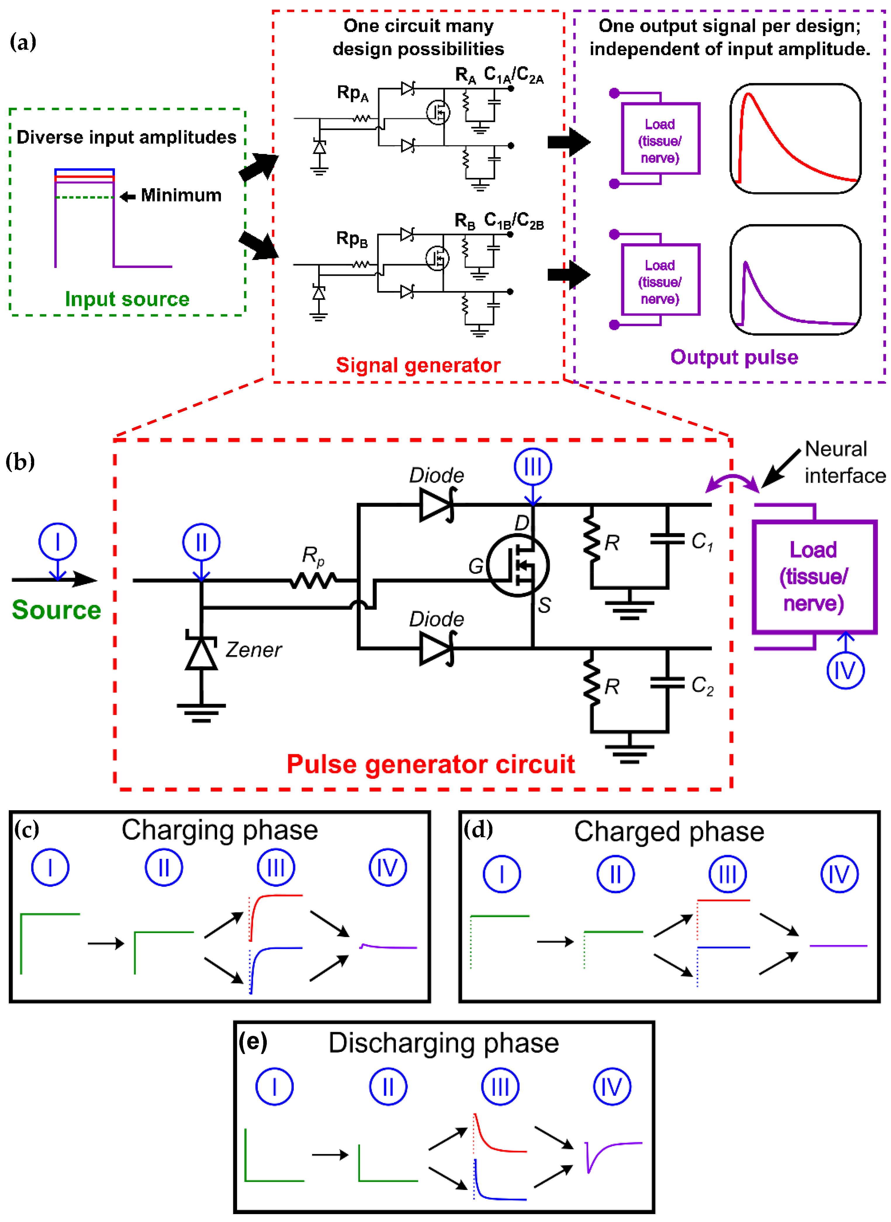
2. Design of Pulse Generation System

2.1. Pulse Generator Circuit Development

The pulse generator circuit is shown in Figure 1a. The pulse generation circuit consists of two resistor–capacitor (RC). We implement control with the input power signal timing to determine when stimulation occurs. The resulting pulse generator outputs a unique waveform according to the passive design components. Output pulses are generated when the input is turned on and then off sequentially. Two output pins are set to a voltage, and then they are discharged at different rates via two capacitors, C1 and C2. This disparity in discharge rates causes the voltage across the tissue between the two electrodes to vary, thus causing stimulation. The output is also connected in parallel to resistors R, which allow passive charge balancing via a direct path to the ground. Grounding with respect to the tissue is not required because the output signal is generated by the variation in voltages between the two output electrodes, and not by reference to the device ground. This method contrasts with the previously described literature, where digital control circuits are employed to provide control of the output signal. However, recording applications may require a different grounding arrangement to obtain reliable measurements. The stimulation target has a path to ground via the resistors R and the electrodes. Circuit output pulse can be accurately designed according to specific requirements. Passive components are used because they allow a simple design and benchtop implementation for verification of the pulse outputs, in addition to a MOSFET. The output of the circuit is regulated such that it is not dependent on variations in the input source, as long as the input supplies a minimum power to generate the output pulse.
The circuit implements regulation of the output voltage in two methods: the input voltage is regulated via a zener diode, and the output pulse amplitude can be modified via a resistor (Rp) placed before the RC branches. The Rp resistor effectively forms a voltage divider with the resistors (R) in the RC branches. Design of the maximum output pulse amplitude is achieved by varying the Rp resistor without affecting the transient response of the RC branches.

2.2. Safety and Failure Modes

As shown in Figure 1b, the RC branches that generate an output pulse, and this voltage is used as the stimulation across the load tissue. These RC branches are isolated through diodes, while still being connected through the load. The layout of the circuit is designed to be inherently safe. The diodes can fail to stay shorted or open circuit. In the case of diodes failing into a short, no signal would be seen by the load, as the terminals across the load would be connected to the same node. If the diodes fail into open circuit, then there would also be no output at the load, since the output would be isolated from the input. It is unlikely that the separate diodes would fail in different modes, since the diode anodes are connected to the same node. A transistor connects the two RC branches, in order to attenuate the charging phase voltage by providing a current path between the RC branches only during the charging phase. The transistor operates in saturation mode when power is supplied to the circuit. In case of transistor failure into a short circuit, there would be no signal at the load, since the terminals across the load would be shorted together. The output electrodes can be driven at high voltage safely because the electrode voltage is in reference to the device ground. The device does not have to be grounded in the target tissue. This feature allows high voltage to be used if desired because the tissue will not be affected by the high voltage to which the capacitors are charged.

2.3. Signal Generator Operation

The signal generator has four distinct phases of operation: the charging phase, the charged phase, the discharging phase, and the unpowered phase, which are outlined in Figure 1c–e. Two phases are important to calculate the pulse: a charging phase when power is supplied to the input, and a discharging phase when power is disconnected.
During the charging phase, the input voltage is isolated and applied separately across each capacitor by diodes. The capacitors are charged to a fixed voltage. This voltage is determined by the voltage regulator and the voltage divider between Rp and R resistors. There is a negligible output signal during the charging phase. The effect of this output signal is reduced with the MOSFET connecting the RC branches, and via passive charge balancing through the resistors R. The charged phase begins once the capacitors are fully charged, and there is no output signal during this phase. Upon triggering the discharging phase by disconnecting the input power, the capacitors are discharged at different rates, making it possible to utilize the discharging potential difference across the capacitors to produce a pulse signal. The last unpowered phase consists of no input signal and no output signal from the circuit. The circuit operates as negative-edge triggered.

2.4. Pulse Design Considerations

The pulse signal parameters that have to be chosen for a given application are waveform, amplitude, width or duration, and output stimulation frequency [24,31]. In our circuit, components in the RC branches (R, C1, and C2) determined the temporal pattern, the amplitude, and the shape of the output waveform. Different C1 and C2 values were chosen in order to accentuate the potential difference between the RC branches. Thus, by varying the capacitances and resistances, it is possible to generate unique output pulse waveforms with different amplitudes, durations, and shapes.
Other considerations can be taken with respect to the stimulation signal waveform. Signal waveforms can be mono- or biphasic. Biphasic signals can be symmetric or asymmetric, and charge-balanced or imbalanced. Waveform phase refers to stimulation signal polarity, and the waveform becomes positive, negative, or both during one stimulation cycle. Waveform symmetry means that the positive and negative phases are identical. Charge balancing is known to reduce probable injury caused to the target tissue due to charge accumulation [32], however, charge-imbalanced or monophasic signals have shown safe and effective results in clinical studies with transcranial pulsed current stimulation applications [33,34], and transcranial magnetic stimulation [19,35,36]. Asymmetric signals have shown selective activation of nerves with a long, small amplitude negative signal followed by a faster, large amplitude positive signal [10,37]. The current circuit design outputs pulse shapes that constitute monophasic and asymmetric signals. It could be possible to generate biphasic symmetric signals by flipping the electrodes via a multiplexer or by using two generators in tandem, but we decided to focus on the pulse generator design in this work. The stimulator circuit and pulse design has inherent safety advantages. The charge delivered can be calculated if the load tissue characteristics are known. The variability in signal design allows for different charge densities according to component design, and electrode and tissue interface selection. Charge density requirements have to be met for each application with the use of this stimulator. Depending on the waveform, the signal is considered effective only when it is above a certain amplitude [16]. This effect is taken into consideration in the circuit analysis when finding the signal stimulation width.

3. Circuit Analysis

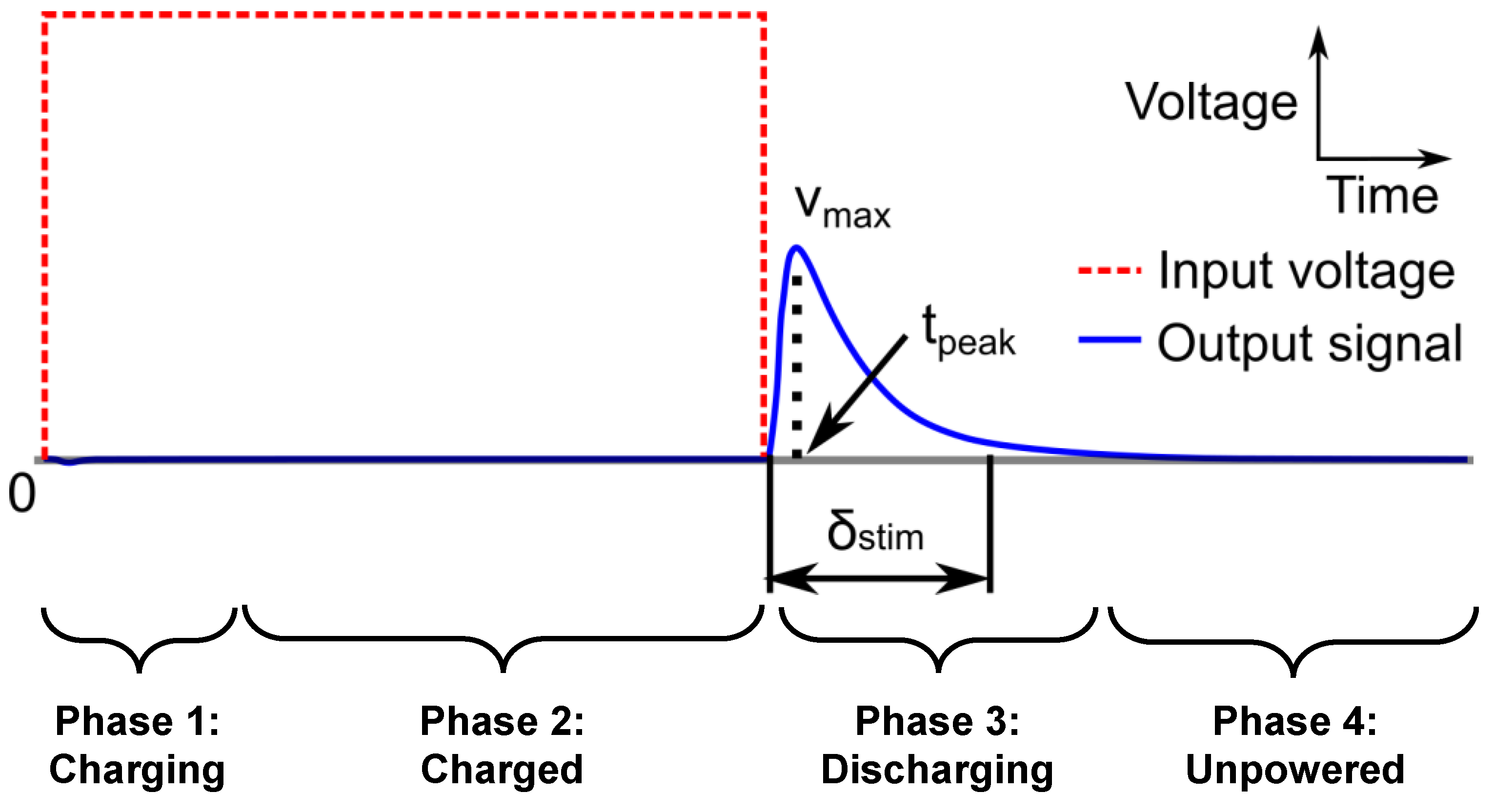
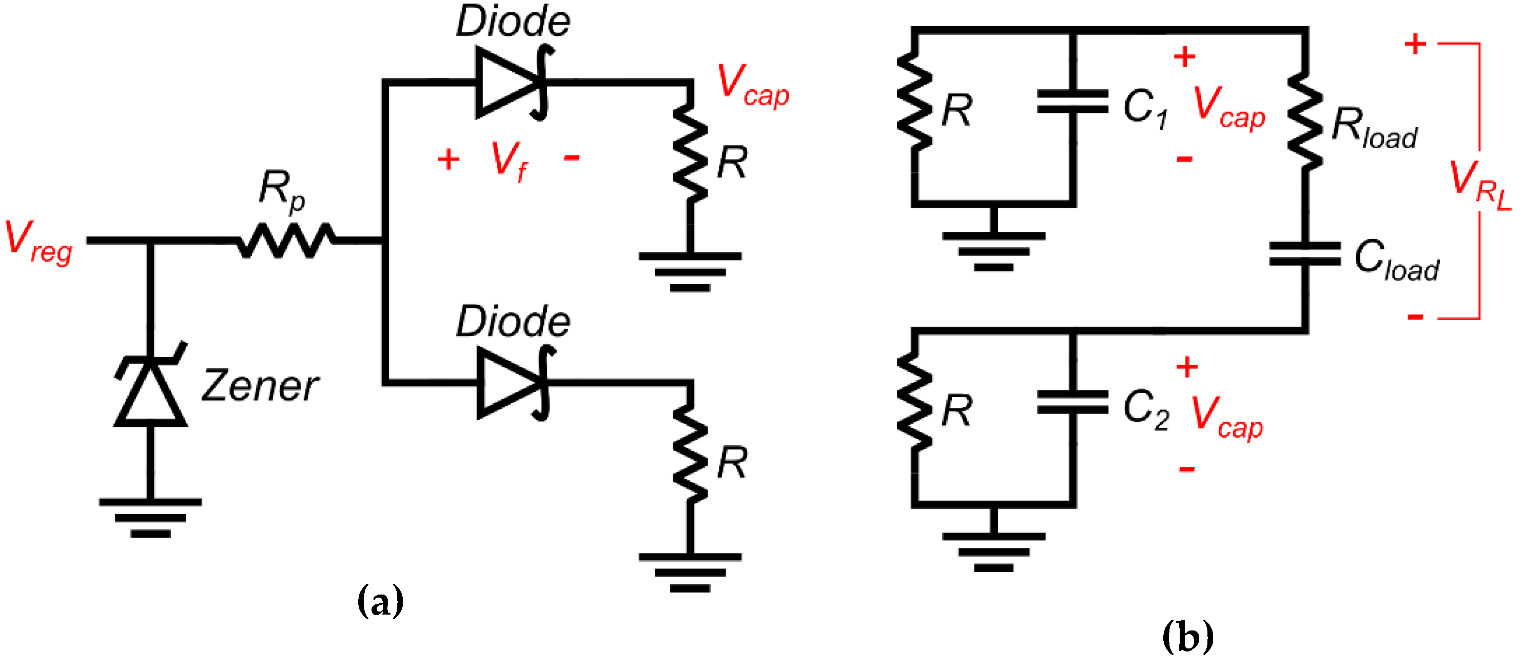
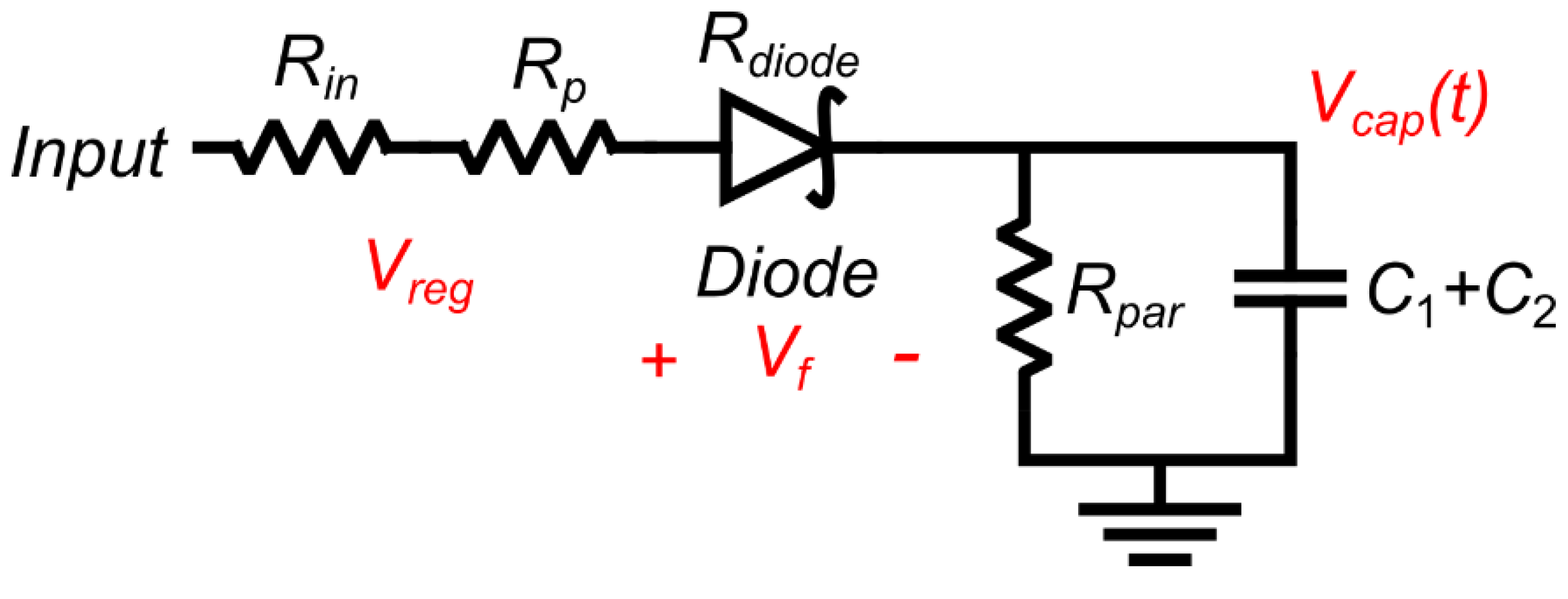
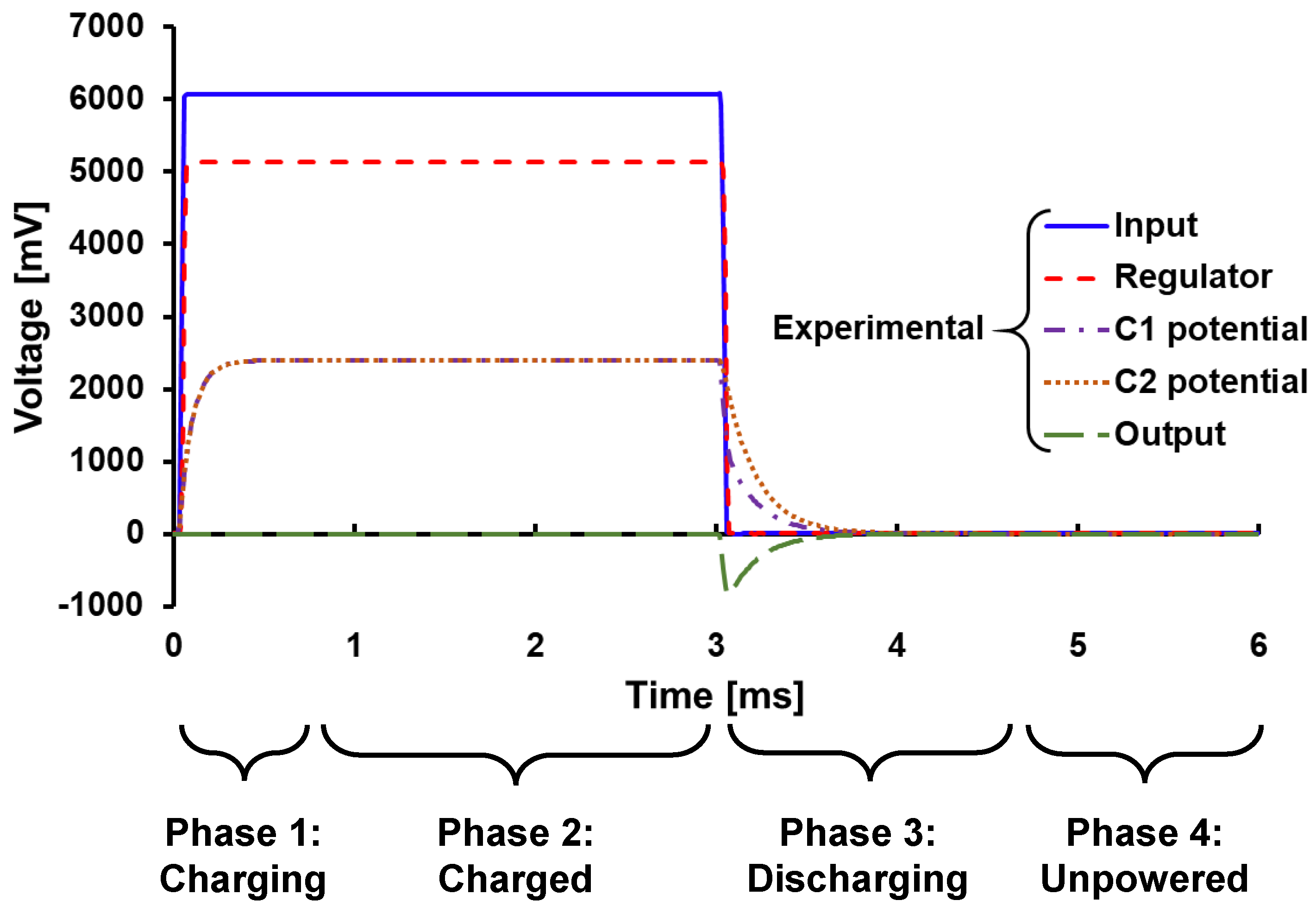
3.1. Overview of Circuit Analysis

We developed an analytical expression to find useful parameters from the output pulse. These parameters are peak amplitude (vmax), peak time (tpeak), and stimulation duration (δstim), as illustrated in Figure 2. When the circuit is powered and cycled through all four phases, it generates one pulse during the discharging phase, thus it is negative-edge triggered. The discharging phase begins when the input signal is disconnected, such that control of the output is achieved by turning the input on and then off. Ideally, there is no signal during the charging, charged, and unpowered phases of operation. We focus our analysis on the charged and discharging phases.
Analysis of the circuit gives us the output function, and this in turn allows us to approximate the design parameters previously mentioned. The analysis consists of two parts: finding the charged phase capacitor voltage, and then the discharging phase output pulse waveform.

3.2. Charged Phase Capacitor Voltage

The capacitor voltage is rising during the charging phase. Then, in the charged phase, the capacitors are fully charged and act like open circuits. The charged phase circuit model is shown in Figure 3a.
The voltage regulator is providing a voltage Vreg, and the diodes are in forward bias with a voltage Vf. The value of interest is the voltage across the resistors R, which is the voltage to which the capacitors are charged Vcap. We found Vcap by solving the voltage divider between Rp and R such that:
V cap = ( V reg V f ) 0.5 R 0.5 R + R p
The value of Vcap is only determined by the resistor values (Rp and R), and is the initial condition for the discharging phase.

3.3. Discharging Output Waveform

During the discharging phase, the diodes are in reverse bias, acting as an open circuit. The RC branches of the circuit are connected through the load and ground during the discharging phase. The load is modeled using a modified Randles model that is a resistor and capacitor in series [29,38,39] (Figure 3b). The effects of the electrode should be incorporated into this model, and the electrode shape and material will determine the electrode equivalent resistance and capacitive double layer. The capacitor represents the electrode–electrolyte double layer capacitance, and bulk capacitance of the tissue.
During the discharging phase, the voltage is supplied only by the capacitors that are each charged to voltage Vcap. The discharging phase output pulse ( v R L ) is a function of R, C1, C2, RL, CL and Vcap. We can apply a simplification where we relate the separate RC time constants of the RC branches. We obtain this ratio by defining κ = RC1/RC2 = C1/C2. Thus, we obtain an output voltage waveform across the load:
v R L ( t ) = v cap ( κ 1 ) C L 2 C 2 R L 2 R κ ( e r 1 t ( C L R L r 1 + 1 ) 2 ( r 1 r 2 ) ( r 1 r 3 ) ( r 1 r 4 ) e r 2 t ( C L R L r 2 + 1 ) 2 ( r 1 r 2 ) ( r 2 r 3 ) ( r 2 r 4 ) + e r 3 t ( C L R L r 3 + 1 ) 2 ( r 1 r 3 ) ( r 2 r 3 ) ( r 3 r 4 ) e r 4 t ( C L R L r 4 + 1 ) 2 ( r 1 r 4 ) ( r 2 r 4 ) ( r 3 r 4 ) )
where Vcap is the voltage to which C1 and C2 are initially charged. We also have r constants that are the roots of a polynomial defined by the values of the design parameters. The output voltage amplitude is directly proportional to Vcap, and thus will be a fraction of the input voltage. This property should be considered when choosing the maximum output voltage amplitude, since this will change depending on the application. Additionally, since Vcap is proportional to the input voltage, it is possible to arbitrarily increase the output voltage by increasing the input voltage and utilizing components rated for the increased circuit voltages.
Knowing (2), we can define the operational parameters of the circuit: tpeak, vmax, δstim. The tpeak for the discharging signal can be found by taking the output signal expression (2) and taking its derivative, which is set equal to 0. The pulse peak amplitude can be found using the value of tpeak and evaluating (2) at that value such that:
v max = v R L ( t peak ) .
Using (3) it is possible to design circuit components according to pulse amplitude requirements. However, it is hard to determine the effects of r in (2) explicitly, due to the complexity of the terms. Since the r constants appear in the exponential terms of (2), it is thought that these constants are a form of time constant for the circuit, playing a significant role in determining δstim. It can be seen that they directly determine tpeak. The pulse duration can be defined as the amount of time it takes for the pulse to rise from 0 ( v R L ( 0 ) = 0 ) up to a pulse peak (vmax), and then decay until it reaches 0 ( v R L ( ) = 0 ). However, we choose to take the pulse duration to be the time the pulse is above a fraction of the amplitude [16]. This is represented with the factor α (0 < α < 1), and can be modified as necessary. We use the value of (3) to find the time tstim when the output signal is a fraction of vmax, denoted by:
v R L ( t stim ) = α v max .
There are two solutions to (4). We take the difference between these two solutions to determine δstim, such that:
δ stim = t decay t rise
where trise is the value of (4) as the pulse increases in magnitude, and tdecay is the value of (4) as the pulse decreases in magnitude.

4. Power Consumption Analysis

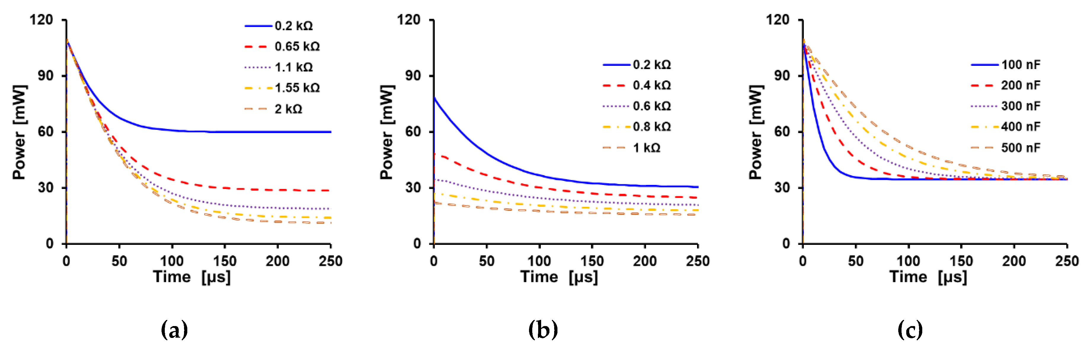
4.1. Overview of Power Analysis

Power analysis is important to understand in what ways the circuit can be optimized for applications that rely on low power consumption, such as implantable, wearable, or portable devices. We show that the most power-efficient strategy is to shorten the length of the charged phase, and lower the effective series resistance (ESR) of the current path to the RC branches. Our analysis is validated with digital simulation in software TINA-TI version 9.3.100.244 (DesignSoft, Budapest, Hungary).

4.2. Ideal Charging Case

To estimate the power, we must know how long the capacitors C1 and C2 will be charging for. The resistance along the current path to the capacitors is the ESR of the source, regulator, and the Rp resistor, in series with the ESR of the diodes. We call this resistance Rinput. We assume the ESR of the attenuation MOSFET to be 0, ideally. The R resistors form a parallel network with each other, Rpar, with Rinput, and are parallel to the capacitors. The equivalent circuit is shown in Figure 4. The time constant of the capacitors during the charging phase can be approximated by:
τ = ( R i n p u t R p a l ) R i n p u t + R p a l ( C 1 + C 2 ) ,
and the time required to charge the capacitors can be approximated to 3τ.
The total power is equivalent to the power consumed by the Rp resistor, diodes, R resistors, and the power required to charge C1 and C2. The Rdiode voltage is known, and the capacitor Vcap(t) follows the capacitor charging equation, with Vcap from (1) as the charging voltage. The maximum current drawn by the circuit is Vcap/Rpar and follows the capacitor current equation:
I i n ( t ) = V c a p R p a r e - t τ ,
and we can determine all the currents and voltages in order to calculate the time-varying power consumption of the circuit.
The total power required to charge the capacitors depends on the C1, C2, and Vcap values. Part of the power dissipated will always be consumed in the resistors in the pulse generator circuit. Power consumption can be reduced by targeting ideal conditions, where the ESR of the diodes and attenuation MOSFET are minimized. Power consumption during the charging phase is not affected by the load conditions if the attenuation MOSFET ESR is very small. Methods to reduce the power consumption include increasing the values of the R resistors, although this also affects the output function, as shown in (2), so optimization can be performed with the signal requirements as constraints. Lowering the value of C1 plus C2 also reduces power consumed during the charging phase and lowers the rate constant, reducing the duration of the charging phase. However, the capacitors similarly affect the output signal and should be optimized with that consideration. Increasing Rp reduces power consumption overall, however, it has the detrimental effect of reducing Vcap, thus directly changing the output signal amplitude. Overall, the power consumption of the charging phase falls as the capacitors are charged and reduces to a minimum constant power when the capacitors are fully charged. The trends were simulated and can be observed in Figure 5.

4.3. Charged and Discharging Phase Analysis

Power consumption during the charged phase is the power consumed by the Rp resistor, diodes, and R resistors. However, as soon as the capacitors are charged, the discharging phase can be initiated. The charged phase can be set to any duration in order to reduce power consumption. Thus, it is recommended that the duration be reduced via smart control methods to prevent any excess power consumed.
The discharging phase does not consume input power. The amount of power delivered to the load follows the same function as (2), and can be optimized in the same manner. Increasing the amplitude of (2) will increase the power delivered and consumed.

5. Characterization Procedures of the Pulse Generator

The circuit was constructed to verify correct operation, and analytical results were compared with measured outputs. Output pulses ( v R L ), and circuit voltages were captured using a Keysight EDUX1002A oscilloscope (Keysight Technologies, Santa Rosa, California, USA). The pulse was obtained by measuring the voltage of each capacitor separately, and then subtracting one signal from the other. The deviation was calculated as the percent difference between the measured experimental value and analytical expression result, divided by the measured experimental value.
First, the circuit operation was verified by capturing the input pulse, the regulated voltage and the capacitor voltage, and the output pulse was found by calculating the difference between the capacitor signals (Figure 6). Subsequently, characterization was performed to verify the accuracy of the analytical expressions and parameter functions by characterization with various components. The values of the components tested are listed in Table 1.
Human internal resistance values have been measured at 0.43–0.56 kΩ, and the electrode resistance values have been reported to vary between 0.5 kΩ and 1.5 kΩ [40,41]. The effect of RL and CL was characterized to understand the effect of load impedance on output. Load resistance values tested range from 500 Ω to 2.7 kΩ [29], and load capacitance values tested are between 27 and 150 nF [38]. Resistor R was characterized to understand the effect of varying R on δstim and the vmax. The Rp characterization was performed to verify that modifying Rp only changes vmax. It is not necessary to increase C1 with respect to C2, as the pulse generator RC branch circuits are symmetric, and doing so would generate pulses with the same shape but opposite polarity. The output pulse frequency was characterized by driving the output pulses at increasing frequencies until the pulse peak vmax breaks down. The output of the circuit was measured in 1X phosphate-buffered saline solution (PBS). Two 220 µm-thick steel needles were dipped 5 mm into the solution, and separated by 5 mm distance and used as the output electrodes of the circuit, and the C2 and R characterization procedures were repeated. The leads were connected to the steel coil section of the needles. The largest output of the circuit was used to estimate the values of CL and RL of the PBS solution using Matlab software (Mathworks, Natick, MA). The circuit is designed to not be limited by choice of electrode, and the needles were chosen for ease of use.
The input timing was generated with an arbitrary function generator (GW Instek AFG 2225, Good Will Instrument Co., Ltd., New Taipei City 236, Taiwan). The input was obtained by programming the pulse setting of the function generator with 50 Hz frequency and 6 V amplitude. The frequency was varied from 20 Hz–2.5 kHz for the frequency limit characterization only. The zener diode regulator had a 5.1 V of zener breakdown voltage. Characterization results were used to verify the accuracy of tpeak, vmax, and Vcap, by comparison with the results of the circuit analysis.

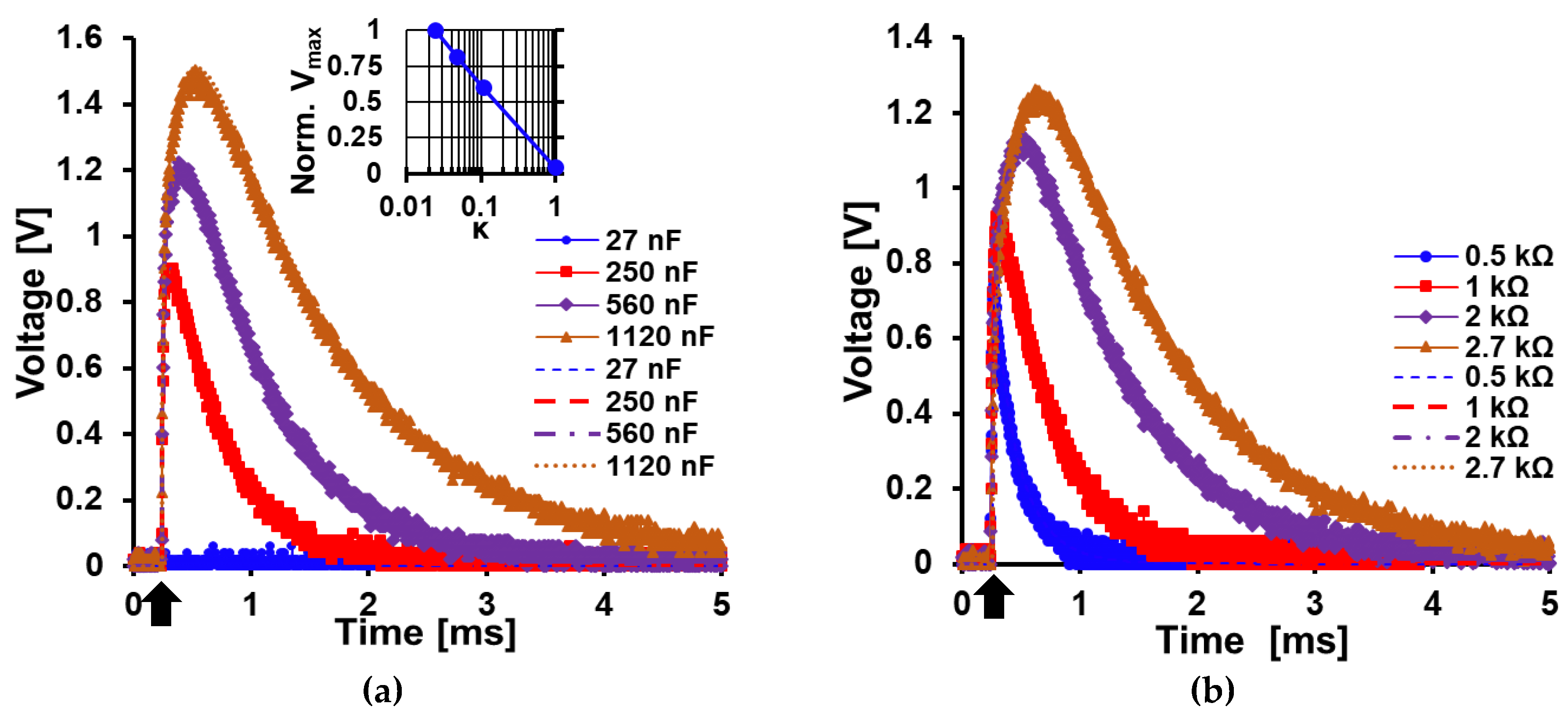
5.1. Analytical Expression Characterization and Validation

The circuit was verified to operate according to the design. The four phases of operation can be observed, and the state of each section of the circuit (I–IV in Figure 2 and Figure 6) was measured to compare with the expected outcome.
The characterization results when C2 was increased are shown in Figure 7a. The component values are C1 = 27 nF, R = 1 kΩ, Rp = 0.5 kΩ, load capacitance 100 nF, and load resistance 1 kΩ. The deviation between measured and calculated values for tpeak is 3.2% to 18.6%, for vmax is less than 1.04%, for δstim is 6.67% to 27%, and for Vcap is 0.17% to 0.35%. Figure 7b shows results where R is increased. The component values are C1 = 27 nF, C2 = 250 nF, Rp = 0.5 kΩ, load capacitance 100 nF, and load resistance 1 kΩ. The deviation between measured and calculated values for tpeak is 0.5% to 48%, for vmax is 0.27% to 3.78%, for δstim is 3.89% to 20.5%, and for Vcap is 1.89% to 6.86%. The output when Rp was increased was also recorded. The component values are C1 = 27 nF, C2 = 250 nF, R = 1 kΩ, load capacitance 100 nF, and load resistance 1 kΩ. The deviation between measured and calculated values for tpeak is 1.72% to 33.7%, for vmax is 5.28% to 11%, for δstim is 2.74% to 20.47%, and for Vcap is 3.97% to 10.95%. A significant component of the error can be attributed to measurement instability of the oscilloscope that contains high-frequency noise which can be observed in the measured output.
The measured output signal is shown to match the analytical expression output in Figure 6 and Figure 7. Deviation in the maximum output voltage vmax was calculated to range from 0.27% to 11% across all characterization tests. The measured and analytical expression values for tpeak had deviations of 1.72% to 48%, and for δstim of 2.74% to 20.5%. The tpeak and vmax, and δstim are difficult to acquire exactly, as a sample may be collected with a slight increase or decrease in amplitude from the actual values for tpeak, δstim, and vmax. The practical effect of the large measured tpeak deviation is minimal, as it can be observed in Figure 7 that the mathematical model waveform closely follows the measured experimental waveform. The Vcap calculation also matched the measured results, with a deviation of 0.17% to 10.95%. The analytical expression is accurate and reliable when designing to meet a given output pulse requirement. The value κ relates the different time constants of each RC branch. In the special case that κ equals 1, it can also be shown conceptually that both RC branches share the same time constant, and thus the pulse becomes 0 across the load. The κ constant is useful to relate the time constant of both RC branches. The expression (2) also holds when C1 is exchanged with C2, and it can be shown by evaluation that the constant parts of the expression are identical but opposite in sign when this change is performed. So when the capacitors are exchanged, the same output signal is generated, except it has opposite polarity.
A similar trend as the one previously mentioned for κ can be seen when R is increased (Figure 7b). This trend also follows the mathematical relationship previously established in (2), whereas when R is increased, the denominator decreases much faster than the numerator, which yields a larger signal. This is similar to how C2 affects the output signal.
Rp varies the maximum amplitude of the output signal without changing the waveform. In summary, the design components R, Rp, C1, and C2 allow for tuning of the output signal amplitude, duration, and location of the peak.

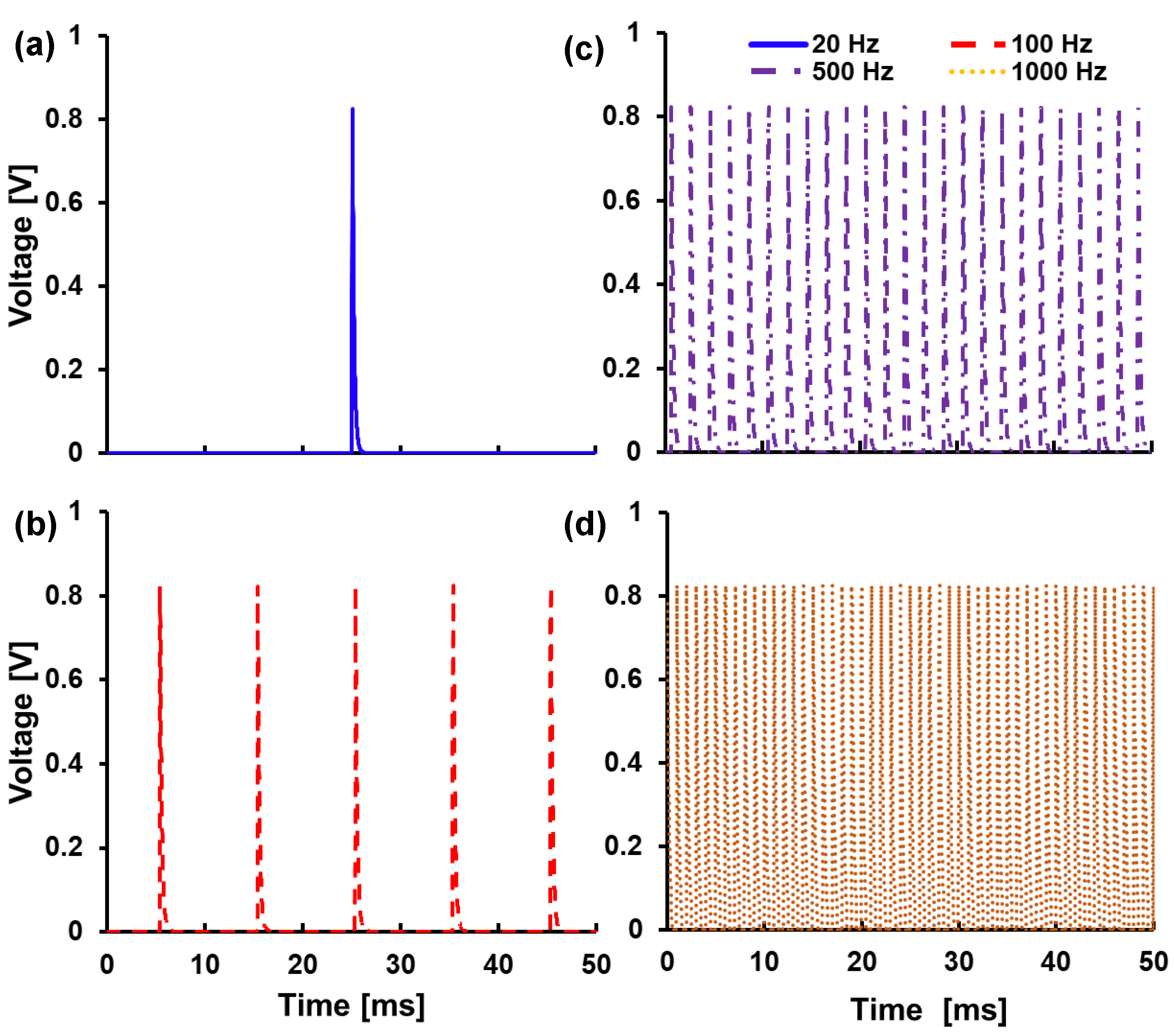
5.2. Output Frequency Characterization

The circuit is also able to operate at different output stimulation frequency levels. The output pulse is shown up to 1 kHz (Figure 8). The output stimulation frequency (fstim) was approximated from the experimental data. The capacitors must first be charged completely during the charging phase before a signal can be generated during the discharging phase. The duration of the charged and unpowered phases can be reduced by control of the input signal, such that they do not appear in the output signal. From the measurement of a low frequency pulse, an expression was derived to approximate the output stimulation frequency limit. First, the charging time of the capacitors, tcharge, is approximated by measuring the duration of the charging phase, which in this case was approximately 500 μs. The experimentally derived fstim becomes:
f s t i m = 1 2 t c h a r g e
This expression allows us to approximate the fstim that a circuit can operate at with given design components. The design components were Rp = 0.5 kΩ, R = 1 kΩ, C1 = 27 nF, and C2 = 250 nF. The circuit is shown to have a reliable fstim variability that is dependent on the width of the charging phase. An exact expression for fstim was not derived in this work. The circuit was tested at frequencies of up to 2.5 kHz, and the circuit operated normally up to 1.6 kHz, where a drop of 1% is seen in vmax. The signal was considered to break down when the vmax amplitude of the output signal was lowered by more than 1% at a given fstim.

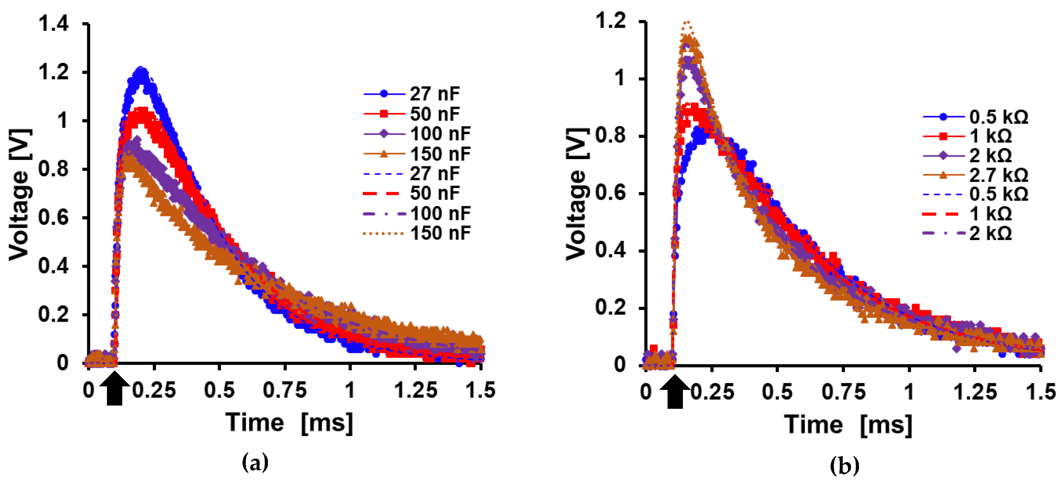
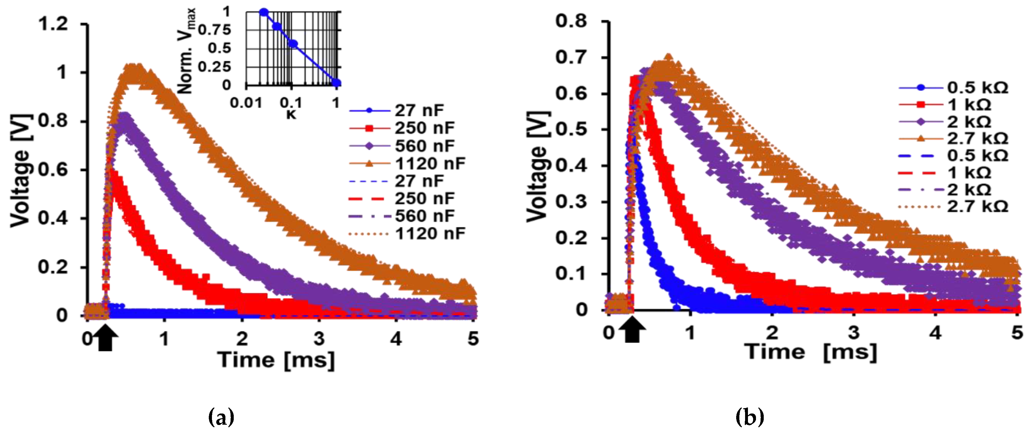
5.3. Load Characterization

The effects of a model load were characterized by varying the load resistance and capacitance (Figure 7). From (2) we can see that the output pulse decreases with increasing load capacitance, and increases with increasing load resistance.
The characterization when the CL is varied is shown in Figure 9a. The design component values are C1 = 27 nF, C2 = 250 nF, R = 1 kΩ, Rp = 0.5 kΩ, and load resistance is 1 kΩ. The deviation between measured and calculated values for tpeak is 5.56% to 10.91%, for vmax is 0.94% to 3.86%, for δstim is 3.92% to 13.98%, and for Vcap is 4.48% to 4.95%. The characterization results when the RL is varied are shown in Figure 9b. The design component values are C1 = 27 nF, C2 = 250 nF, R = 1 kΩ, Rp = 0.5 kΩ, and load capacitance is 100 nF. The deviation between measured and calculated values for tpeak is 6% to 32.94%, for vmax is 0.20% to 5.01%, for δstim is 8.86% to 20.2%, and for Vcap is 4.95% to 5.81%. The load conditions affect both the tpeak and vmax, however, the signal width δstim was affected in a different manner. Since δstim depends on vmax in our definition, the output width is affected according to our analytical expression.
Observation of the measured results suggests that variations in RL do not significantly affect the signal after the time point tpeak, and the effects of the resistive load on the tail end of the signal are minimal.
The charge delivered to the load can be approximated with:
Q stim = t rise t decay I load ( t ) dt
where the current across the load is defined by the voltage across the load and the electrode parameters.
Power consumption analysis of the circuit is not the focus of this work, however, the target application should be considered when designing the circuit. Laboratory studies that focus on analyzing in vitro tissue responses to diverse waveforms will have different power requirements than in vivo studies with wearable devices such as transcranial electrical stimulation (TES) and functional electrical stimulation (FES). Studies related to the effects of waveforms in vitro have less strict power requirements when compared to portable devices in vivo.

5.4. PBS Solution Measurements

The design of the circuit has to take into account the target application load conditions. The circuit output was measured when electrodes and PBS solution were used as the load instead of the circuit model load. The electrodes are considered part of the load when using (2). The largest signal of each data set (1120 nF for C2 characterization, and 2.7 kΩ for R characterization) was curve-fit using (2) to estimate the component values of the circuit model load, and these values were then used to calculate the output of the circuit analytical expression for the other component values used for characterization. The load component values were estimated to be CL = 410 nF and R = 600 Ω for the C2 characterization (Figure 10a), and CL = 310 nF and R = 580 Ω for the R characterization (Figure 10b). The characterizations performed in PBS solution load showed the same trends as the electrical model load characterization.
The characterization for C2 in PBS solution load had design component values C1 = 27 nF, R = 1 kΩ, and Rp = 0.5 kΩ. The deviation between measured and calculated values for tpeak is 8.9% to 75%, for vmax is 3.5% to 11.8%, and for δstim is 25.7% to 61%. The characterization for R in PBS solution load had the design component values C1 = 27 nF, C2 = 250 nF, and Rp = 0.5 kΩ. The deviation between measured and calculated values for tpeak is 9.67% to 69%, for vmax is 1% to 15.3%, and for δstim is 15.5% to 48.7%. The output signal in PBS solution can be estimated using the output expressions of the circuit and one measurement. The measured output was observed to be similar to the analytical expression output, however, there were time domain discrepancies that led to a high deviation in tpeak values. This indicates that the load model based on the simplified Randles equivalent circuit is incomplete, and can be improved with a better model of the electrode–electrolyte interface. The electrical properties of the tissue load should be properly characterized when developing electrical stimulation devices. This would allow to better determine the effects of stimulation on the target, and the output response on different types of tissue load. The measured results and analytical expression output show good agreement overall, and the output stimulation pulse in future applications can be estimated if the expected CL and RL are found.

6. Conclusions and Future Work

A novel passive pulse generator circuit has been presented and characterized. The signal generator operation and circuit analytical expressions were verified by characterizing an assembled circuit. The analytical expression results and the experimental measured results showed good agreement in both benchtop and PBS solution measurements, which confirms that the circuit expressions are accurate. In terms of signal design, vmax, tpeak, and δstim increased as κ was decreased; and tpeak and δstim increased and vmax decreased as R was increased. The pulse generator outputs a unique shape for each design component combination, allowing for the design of the pulse when given a required amplitude and duration.
An expression for the limit of the output stimulation frequency was derived from the measured results of the signal generator waveform. The pulse generator is independent of tissue interface, and was designed to be coupled with different power sources and neural interface mechanisms for application-specific purposes. The power consumption of the circuit should be considered when designing a circuit for specific applications. Knowing the electrode type and target tissue (muscle, nerve, brain slices), an application-specific circuit could be designed using the analytical circuit expressions. Improvements to the model, to find the charge density provided by the signal generator with a given neural interface, are also possible. It is envisioned that this system could be used as a research tool in studies of stimulation waveforms and their effects on neuromodulation.
Current work is focused on methods for biphasic signal generation. Additional improvements include the implementation of a closed-loop feedback circuit to regulate the output pulse according to changing load conditions, and this addition may be necessary for long-term applications. In vitro and in vivo stimulation studies could be implemented in order to demonstrate the applicability of this circuit in neurostimulation. The effectiveness of our passive charge balancing method via continuous grounding should be verified with further studies on tissue damage. An implantable device would have to take into consideration the size of the passive devices on the circuit, as these may be large depending on the implant location.

Author Contributions

A.P. worked on the conceptualization, methodology, validation, and writing of the initial draft, J.-W.C. performed critical review and editing of the draft, supervision, and project administration.

Funding

This research was funded in part by Louisiana State University Economic Development Assistantship, Leveraging Innovation for Technology Transfer Grant (LSU-2019-LIFT-010), and Louisiana Board of Regents (LEQSF(2019-20)-RD-D-03).

Conflicts of Interest

The authors declare no conflict of interest.

References

  1. Reato, D.; Rahman, A.; Bikson, M.; Parra, L.C. Low-intensity electrical stimulation affects network dynamics by modulating population rate and spike timing. J. Neurosci. 2010, 30, 15067–15079. [Google Scholar] [CrossRef] [PubMed]
  2. Hoppa, M.B.; Gouzer, G.; Armbruster, M.; Ryan, T.A. Control and plasticity of the presynaptic action potential waveform at small CNS nerve terminals. Neuron 2014, 84, 778–789. [Google Scholar] [CrossRef] [PubMed]
  3. Orsborn, A.L.; Moorman, H.G.; Overduin, S.A.; Shanechi, M.M.; Dimitrov, D.F.; Carmena, J.M. Closed-loop decoder adaptation shapes neural plasticity for skillful neuroprosthetic control. Neuron 2014, 82, 1380–1393. [Google Scholar] [CrossRef] [PubMed]
  4. Shenoy, K.V.; Carmena, J.M. Combining decoder design and neural adaptation in brain-machine interfaces. Neuron 2014, 84, 665–680. [Google Scholar] [CrossRef] [PubMed]
  5. Bostrom, N.; Sandberg, A. Cognitive enhancement: methods, ethics, regulatory challenges. Sci. Eng. Ethics 2009, 15, 311–341. [Google Scholar] [CrossRef] [PubMed]
  6. Schambra, H.M.; Abe, M.; Luckenbaugh, D.A.; Reis, J.; Krakauer, J.W.; Cohen, L.G. Probing for hemispheric specialization for motor skill learning: a transcranial direct current stimulation study. J. Neurophysiol. 2011, 106, 652–661. [Google Scholar] [CrossRef] [PubMed]
  7. Sasaki, T.; Matsuki, N.; Ikegaya, Y. Effects of Axonal Topology on the Somatic Modulation of Synaptic Outputs. J. Neurosci. 2012, 32, 2868–2876. [Google Scholar] [CrossRef]
  8. Sasaki, T.; Matsuki, N.; Ikegaya, Y. Action-potential modulation during axonal conduction. Science 2011, 331, 599–601. [Google Scholar] [CrossRef]
  9. Boudkkazi, S.; Fronzaroli-Molinieres, L.; Debanne, D. Presynaptic action potential -waveform determines cortical synaptic latency. J. Physiol. 2011, 589, 1117–1131. [Google Scholar] [CrossRef]
  10. McIntyre, C.C.; Grill, W.M. Extracellular stimulation of central neurons: influence of stimulus waveform and frequency on neuronal output. J. Neurophysiol. 2002, 88, 1592–1604. [Google Scholar] [CrossRef]
  11. Grill, W.; Mortimer, J.T. The effect of stimulus pulse duration on selectivity of neural stimulation. IEEE Trans. Biomed. Eng. 1996, 43, 161–166. [Google Scholar] [CrossRef] [PubMed]
  12. Wongsarnpigoon, A.; Woock, J.P.; Grill, W.M. Efficiency analysis of waveform shape for electrical excitation of nerve fibers. IEEE Trans. Neural. Syst. Rehabil. Eng. 2010, 18, 319–328. [Google Scholar] [CrossRef] [PubMed]
  13. Pell, G.S.; Roth, Y.; Zangen, A. Modulation of cortical excitability induced by repetitive transcranial magnetic stimulation: influence of timing and geometrical parameters and underlying mechanisms. Prog. Neurobiol. 2011, 93, 59–98. [Google Scholar] [CrossRef] [PubMed]
  14. Lang, N.; Harms, J.; Weyh, T.; Lemon, R.N.; Paulus, W.; Rothwell, J.C.; Siebner, H.R. Stimulus intensity and coil characteristics influence the efficacy of rTMS to suppress cortical excitability. Clin. Neurophysiol. 2006, 117, 2292–2301. [Google Scholar] [CrossRef]
  15. Barth, B.B.; Henriquez, C.S.; Grill, W.M.; Shen, X. Electrical stimulation of gut motility guided by an in silico model. J. Neural. Eng. 2017, 14. [Google Scholar] [CrossRef]
  16. Foutz, T.J.; McIntyre, C.C. Evaluation of novel stimulus waveforms for deep brain stimulation. J. Neural. Eng. 2010, 7. [Google Scholar] [CrossRef]
  17. Wongsarnpigoon, A.; Grill, W.M. Energy-efficient waveform shapes for neural stimulation revealed with a genetic algorithm. J. Neural. Eng. 2010, 7. [Google Scholar] [CrossRef]
  18. Chipchase, L.S.; Schabrun, S.M.; Hodges, P.W. Peripheral electrical stimulation to induce cortical plasticity: a systematic review of stimulus parameters. Clin. Neurophysiol. 2011, 122, 456–463. [Google Scholar] [CrossRef]
  19. Kammer, T.; Beck, S.; Thielscher, A.; Laubis-Herrmann, U.; Topka, H. Motor thresholds in humans: a transcranial magnetic stimulation study comparing different pulse waveforms, current directions and stimulator types. Clin. Neurophysiol. 2001, 112, 250–258. [Google Scholar] [CrossRef]
  20. Cassar, I.R.; Titus, N.D.; Grill, W.M. An improved genetic algorithm for designing optimal temporal patterns of neural stimulation. J. Neural. Eng. 2017, 14. [Google Scholar] [CrossRef]
  21. Kuncel, A.M.; Grill, W.M. Selection of stimulus parameters for deep brain stimulation. Clin. Neurophysiol. 2004, 115, 2431–2441. [Google Scholar] [CrossRef] [PubMed]
  22. Magis, D.; Schoenen, J. Advances and challenges in neurostimulation for headaches. The Lancet Neurol. 2012, 11, 708–719. [Google Scholar] [CrossRef]
  23. Cruccu, G.; Aziz, T.Z.; Garcia-Larrea, L.; Hansson, P.; Jensen, T.S.; Lefaucheur, J.-P.; Simpson, B.; Taylor, R.S. EFNS guidelines on neurostimulation therapy for neuropathic pain. Eur. J. Neurol. 2007, 14, 952–970. [Google Scholar] [CrossRef] [PubMed]
  24. Davidovics, N.S.; Fridman, G.Y.; Chiang, B.; Della Santina, C.C. Effects of biphasic current pulse frequency, amplitude, duration, and interphase gap on eye movement responses to prosthetic electrical stimulation of the vestibular nerve. IEEE Trans. Neural. Syst. Rehabil. Eng. 2011, 19, 84–94. [Google Scholar] [CrossRef] [PubMed]
  25. Ahuja, A.K.; Behrend, M.R.; Kuroda, M.; Humayun, M.S.; Weiland, J.D. An in vitro model of a retinal prosthesis. IEEE Trans. Biomed. Eng. 2008, 55, 1744–1753. [Google Scholar] [CrossRef]
  26. Gorman, P.H.; Mortimer, J.T. The effect of stimulus parameters on the recruitment characteristics of direct nerve stimulation. IEEE Trans. Biomed. Eng. 1983, BME-30, 407–414. [Google Scholar] [CrossRef]
  27. Seo, D.; Neely, R.M.; Shen, K.; Singhal, U.; Alon, E.; Rabaey, J.M.; Carmena, J.M.; Maharbiz, M.M. Wireless Recording in the Peripheral Nervous System with Ultrasonic Neural Dust. Neuron 2016, 91, 529–539. [Google Scholar] [CrossRef]
  28. Qian, X.; Hao, H.-W.; Ma, B.-Z.; Wen, X.-W.; Hu, C.-H.; Li, L.-M.; Lau, R.Y.C.; Guo, X. Programmable and implantable neurostimulator with novel stimulus waveforms for rat models. Electron. Lett. 2012, 48, 1035–1036. [Google Scholar] [CrossRef]
  29. van Dongen, M.N.; Serdijn, W.A. A power-efficient multichannel neural stimulator using high-frequency pulsed excitation from an unfiltered dynamic supply. IEEE Trans. Biomed. Circuits Syst. 2016, 10, 61–71. [Google Scholar] [CrossRef]
  30. Khalifa, A.; Karimi, Y.; Wang, Q.; Garikapati, S.; Montlouis, W.; Stanaćević, M.; Thakor, N.; Etienne-Cummings, R. The Microbead: A Highly Miniaturized Wirelessly Powered Implantable Neural Stimulating System. IEEE Trans. Biomed. Circuits Syst. 2018, 12, 521–531. [Google Scholar] [CrossRef]
  31. Zaraska, W.; Thor, P.; Lipiński, M.; Cież, M.; Grzesiak, W.; Początek, J.; Zaraska, K. Design and fabrication of neurostimulator implants—selected problems. Microelectron. Reliab. 2005, 45, 1930–1934. [Google Scholar] [CrossRef]
  32. Lilly, J.C.; Hughes, J.R.; Alvord Jr, E.C.; Galkin, T.W. Brief, noninjurious electric waveform for stimulation of the brain. Science 1955, 121, 468–469. [Google Scholar] [CrossRef] [PubMed] [Green Version]
  33. Vasquez, A.; Malavera, A.; Doruk, D.; Morales-Quezada, L.; Carvalho, S.; Leite, J.; Fregni, F. Duration dependent effects of transcranial pulsed current stimulation (tPCS) indexed by electroencephalography. Neuromodulation 2016, 19, 679–688. [Google Scholar] [CrossRef] [PubMed]
  34. Alon, G.; Roys, S.R.; Gullapalli, R.P.; Greenspan, J.D. Non-invasive electrical stimulation of the brain (ESB) modifies the resting-state network connectivity of the primary motor cortex: a proof of concept fMRI study. Brain Res. 2011, 1403, 37–44. [Google Scholar] [CrossRef] [PubMed]
  35. Lazzaro, V.; Oliviero, A.; Mazzone, P.; Insola, A.; Pilato, F.; Saturno, E.; Accurso, A.; Tonali, P.A.; Rothwell, J.C. Comparison of descending volleys evoked by monophasic and biphasic magnetic stimulation of the motor cortex in conscious humans. Exp. Brain Res. 2001, 141, 121–127. [Google Scholar] [CrossRef] [PubMed]
  36. Di Lazzaro, V.; Oliviero, A.; Pilato, F.; Saturno, E.; Dileone, M.; Mazzone, P.; Insola, A.; Tonali, P.A.; Rothwell, J.C. The physiological basis of transcranial motor cortex stimulation in conscious humans. Clin. Neurophysiol. 2004, 115, 255–266. [Google Scholar] [CrossRef] [PubMed]
  37. McIntyre, C.C.; Grill, W.M. Selective microstimulation of central nervous system neurons. Ann. Biomed. Eng. 2000, 28, 219–233. [Google Scholar] [CrossRef]
  38. Hsu, W.-Y.; Schmid, A. Compact, Energy-Efficient High-Frequency Switched Capacitor Neural Stimulator With Active Charge Balancing. IEEE Trans. Biomed. Circuits Syst. 2017, 11, 878–888. [Google Scholar] [CrossRef]
  39. Lin, Y.-P.; Yeh, C.-Y.; Huang, P.-Y.; Wang, Z.-Y.; Cheng, H.-H.; Li, Y.-T.; Chuang, C.-F.; Huang, P.-C.; Tang, K.-T.; Ma, H.-P.; et al. A Battery-Less, Implantable Neuro-Electronic Interface for Studying the Mechanisms of Deep Brain Stimulation in Rat Models. IEEE Trans. Biomed. Circuits Syst. 2016, 10, 98–112. [Google Scholar] [CrossRef]
  40. Butson, C.R.; Maks, C.B.; McIntyre, C.C. Sources and effects of electrode impedance during deep brain stimulation. Clin. Neurophysiol. 2006, 117, 447–454. [Google Scholar] [CrossRef] [Green Version]
  41. Lukaski, H.C.; Bolonchuk, W.W.; Hall, C.B.; Siders, W.A. Validation of tetrapolar bioelectrical impedance method to assess human body composition. J. Appl. Physiol. 1986, 60, 1327–1332. [Google Scholar] [CrossRef] [PubMed] [Green Version]
Figure 1. Overview of envisioned pulse generator circuitry and pulse generation phases: (a) envisioned pulse generator circuit design; (b) circuit of pulse generator; (c) charging phase where two RC circuits are charged; (d) charged phase with input signal on, and the two RC branch circuits yielding 0 output signal, and (e) discharging phase with input signal turned off, thus causing the two RC branch circuits to discharge and generate the output signal. The last phase is an unpowered circuit, with no signals across the circuitry (not shown). The pulse generator circuitry in (b) consists of an input power source (I), an input voltage regulation circuit (II), RC branches (III), and a load connected to the output (IV).
Electronics 08 01344 g001
Figure 2. An example input and output signal. The discharging phase has peak amplitude (vmax), peak time (tpeak), and stimulation duration (δstim).
Electronics 08 01344 g002
Figure 3. Circuit models for analysis. (a) Charged phase circuit model with capacitors C1 and C2 charged to Vcap; (b) discharging phase circuit model, Vcap is the initial voltage of C1 and C2.
Electronics 08 01344 g003
Figure 4. Charging phase equivalent circuit for power analysis. Rinput is equal to the series resistance comprised of Rin, Rp, and Rdiode.
Electronics 08 01344 g004
Figure 5. Simulations of component effects on input power consumption: (a) varying R, (b) varying Rp, and (c) varying C1 + C2.
Electronics 08 01344 g005
Figure 6. Circuit output showing voltages and four operational phases.
Electronics 08 01344 g006
Figure 7. Measured output to verify analytical expressions: (a) output for increasing C2, or as κ is decreased, and normalized magnitude of vmax against κ (inset); (b) measured output for increasing R. Experimental results in solid lines with markers, analytical expression results in dotted lines. Arrow indicates signal start.
Electronics 08 01344 g007
Figure 8. Measured results with a variable output pulse frequency of (a) 20 Hz, (b) 100 Hz, (c) 500 Hz, and (d) 1000 Hz.
Electronics 08 01344 g008
Figure 9. Measured output with varying load conditions: (a) output for increasing load capacitance; and (b) load resistance. Experimental results in solid lines with markers, analytical expression results in dotted lines. Arrow indicates signal start.
Electronics 08 01344 g009
Figure 10. Measured output with steel needle electrodes in PBS solution: (a) measured output for increasing C2; and (b) increasing R. Experimental results in solid lines with markers, analytical expression results in dotted lines. Arrow indicates signal start.
Electronics 08 01344 g010
Table 1. Circuit characterization components.
ComponentValue
RL [kΩ]0.5, 1, 2, 2.7
CL [nF]27, 50, 100, 150
R [kΩ]0.5, 1, 2, 2.7
Rp [kΩ]0, 0.5, 1
C1 [nF]27
C2 [nF]27, 250, 560, 1120
Input voltage [V]6

