6.1. Introduction
In this section, seven different FPGA FFT implementations are described, with the purpose of demonstrating how the same architecture can be used for a range of applications. The first two designs (
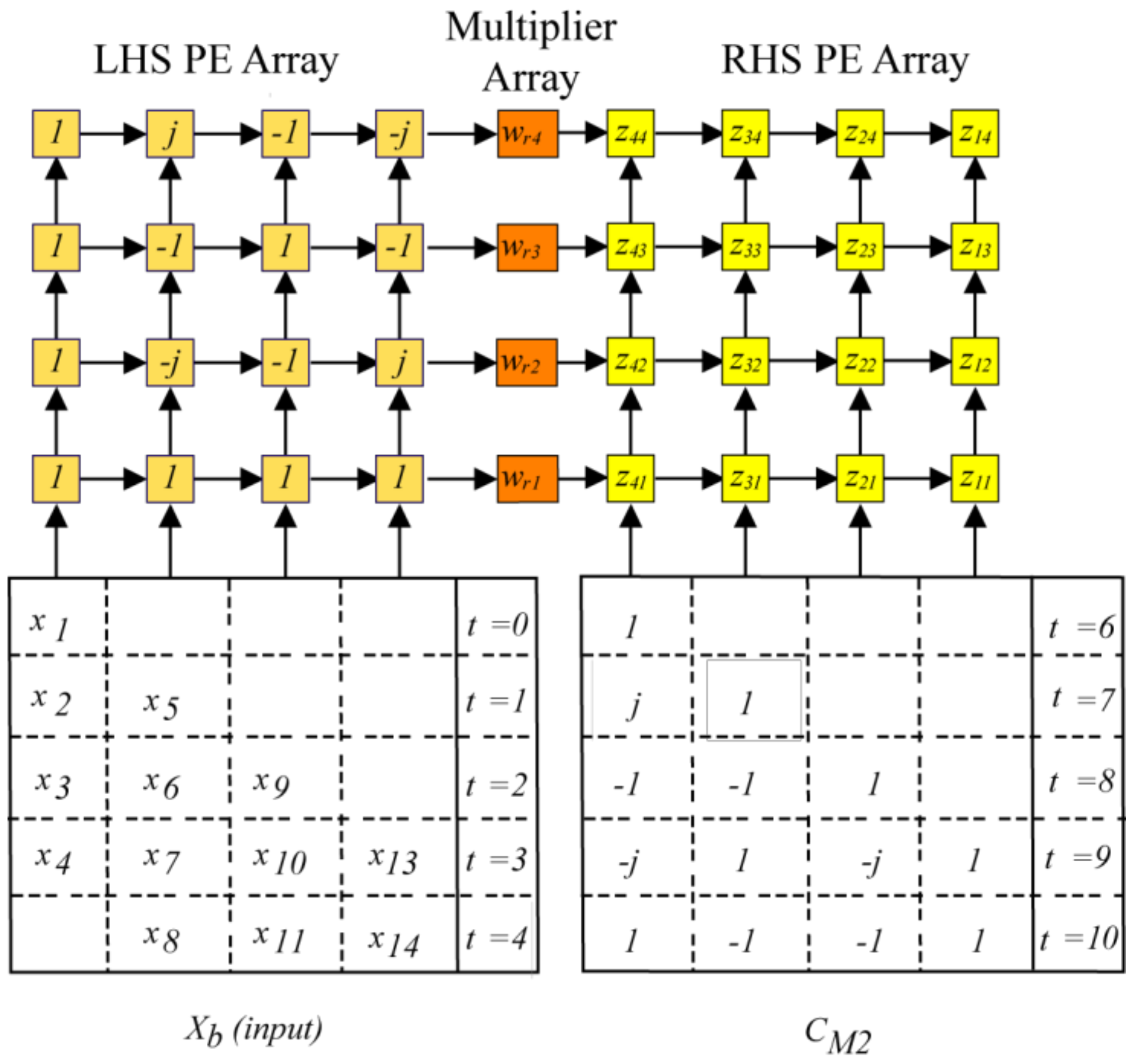
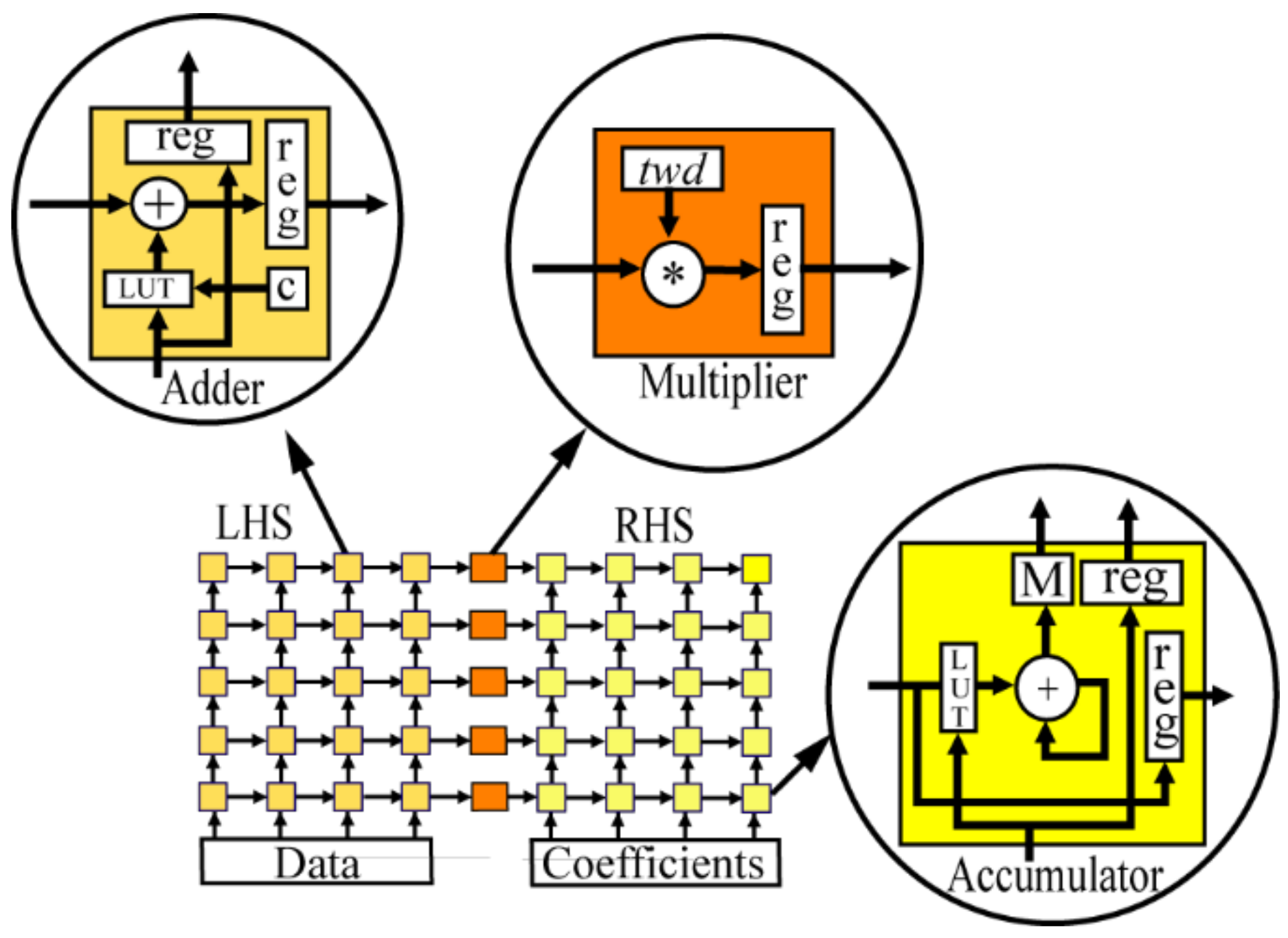
Section 6.2) are fixed-size power-of-two FFTs (256-points and 1024-points) that take computational advantage of the radix-4 butterfly matrix in which case the LHS/RHS PE multipliers are replaced by adders because C
M1/2 contains only {±1, ±
j} (see
Figure 3). The third design (
Section 6.3) is like the first, but adds a requirement for run-time choice of FFT size. The last three power-of-two FFT circuits (
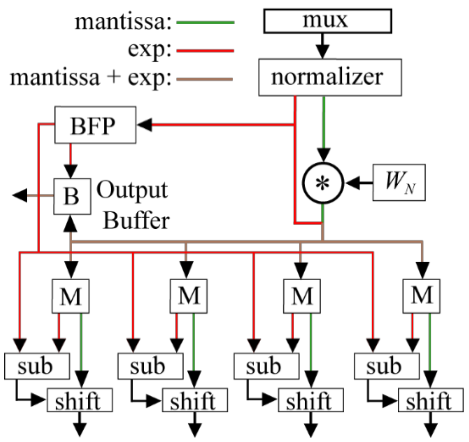
Section 6.4) use single-precision floating-point formats (IEEE 754), one of which targets the latest in FPGA embedded floating-point hardware support. Finally, in
Section 6.5, a complex, non-power-of-two design is presented that uses mixed-radices and offers run-time FFT choice, yet has the a very simple programming model for performing any size of FFT.
Additionally, comparisons to other FPGA implementations are included. This is often difficult because circuit properties can vary considerably, due to the different CMOS technologies/speed-grades, embedded circuit types, LUT/register fabric architecture, FFT functionality, word growth control, circuit architectures, and the FPGA tools and tool settings used. Consequently, the goal was to provide more accurate comparisons by using close to identical circuit functionality, SQNR, target FPGA hardware, tools, and settings as possible. A range of different FPGA types and technologies were chosen to add variety to the comparisons.
Although it is common to compare FFT architectures based on a table with entries representing resources used and transform times as a function of transform size N, this only works well when there is a direct correspondence between N and hardware, as in the case of pipelined FFTs. Memory-based architectures do not share this one-to-one correspondence, so a useful table would be difficult to construct. Additionally, there are many design issues impacting resource usage and speed that cannot be addressed in such tables. Therefore, the focus in this section is on circuitry that has been successfully compiled with the same tool settings, and then simulated and tested using complex random input data followed by comparisons of output data to Matlab generated values. In some cases where noted testing has also been done using FPGA development hardware boards. In this way the comparisons are comprehensive and thus more useful.
In the comparisons with Intel FPGAs, Intel’s Quartus synthesizer, and place-and-route design tools were used, and the Timequest static timing analyzer determined worst-case maximum clock frequencies (Fmax) at 85 C. For Xilinx FPGAs, ISE 14.7 tools for synthesis and place-and-route were used. All Fmax or clock rate values are the same as the complex data sample rate, except where noted, and were obtained by choosing the highest values from at least three different compiler seeds. All SQNR values were calculated using at least 500 blocks of random FFT complex input data. For 16-bit word length input circuits, all twiddle factors were 18-bits, except where noted. Real multipliers were 18-bits, except for the floating-point circuits. All designs support forward and inverse transforms except where noted.
All results include a measure of circuit efficiency, our primary metric of design success, defined by the throughput obtained per logic cell, given terms of registers and LUTs, as follows:
where throughput is expressed in transforms/µs. Another logic cell choice would have been to use slices for Xilinx devices and adaptive logic modules (ALMs) for Altera devices, but this information was not available in many of the circuits used in the comparisons.
6.2. 256-Point and 1024-Point Streaming (Normal Order In and Out) Fixed-Size FFTs
For these two transform sizes, the FFT circuits targeted the same hardware, Stratix III EP3SE50F484C2 FPGAs (65 nm technology) and comparisons are made to Intel [
32], Gird [
33] and Spiral [
34] circuits.
The Intel circuit is based on a mixed radix-4/2 20-bit pipelined FFT that uses BFP (single exponent per FFT block) to achieve a similar SQNR as the DMBA FFT circuits [
32]. The SQNR results for the Intel circuits were obtained from a bit-accurate Matlab model created along with the circuit by the Intel FFT generators (IPv13.1). Here, the ALM is the basic unit of a Stratix III FPGA (two variable size LUTs, two registers, plus other logic). An M9K is a 9216-bit memory with a word length up to 36-bits.
Compared to the Intel circuits,
Table 2 shows that the DMBA FFTs use fewer registers, ALMs, and M9Ks, with throughput rates that are 46%/40% higher for 256/1024-points, leading to better values of throughput per logic cell (7) by 44%/36%. Note that there are significant improvements in power dissipation as well (results obtained from Quartus Power Play Power Analyzer tool). For 256-points, it is possible to use LUTs for the DMBA circuit’s internal memory, so that only 15 M9Ks are necessary. In this case, the number of ALMs would be approximately the same as for the Intel version.
As part of a larger project to automate the development of signal processing algorithms, the Spiral designs come from a parameterized tool that generates Verilog code for fixed-point and floating-point fixed-size power-of-two FFTs. Here, forward, streaming designs with scaling to prevent errors were chosen. Bi-directional transforms were not an option. Like the Intel circuit a higher word length was required for comparable SQNR, obtained from Verilog simulations. Unlike the other designs considered here, the Spiral circuits process two complex words per cycle, so transforms complete in N/2 cycles. The Spiral circuits use fewer LUTs, but more registers, M9Ks and multipliers. So while these circuits achieve marginally better throughputs per logic cell, memory (M9K) and multiplier usage are significantly higher by 42%/245% and ×3.4/×4.4 for the 256/1024-point designs.
In
Table 2, the commercial Gird Systems IP core is a 16-bit, streaming, decimation-in-frequency, radix-4 core and results are shown for an Intel Stratix IV FPGA (EP4SE230C4). The Stratix III and IV FPGAs use different fabrication technologies (65 nm and 40 nm), but their architectures are the same, so the comparisons, except for speed (C4 is a lower speed grade), are somewhat useful. It is important to note that the circuit uses scaling of results in intermediate stages to control word growth, so that likely the SQNR for this circuit is much less than all the other designs in the table. Like the Intel and Spiral designs, if a 20-bit circuit were used, all the Gird resource numbers would increase significantly.
6.3. Variable FFT Streaming (Normal Order In and Out)
In this section, a variable streaming FFT circuit is described that provides a run-time choice of 128/256/512/1024/2048 transform sizes as required for 802.11ax [
4] and LTE protocols [
3]. For this circuit with
b = 4, it was natural to choose a factorization with
N3 = 16 for all transform sizes. This choice leads to simple 4 × 4 SAs, as in
Figure 3 and
Figure 6, for the 16-point column transforms with processing based on (3). All the desired twiddle factors
WN can be conveniently found among the elements of
W2048.
After the column DFTs, it would be possible to perform each of the
N4-point row transforms using (3) exclusively; however, better efficiency is achieved by factoring some of the row DFTs again (
N4 =
N5N6) and differently for each transform size, so row DFTs are broken into two steps. The rows in
Table 3 show how each DFT transform of the 16 DFT matrix rows of length
N4 is performed in the SAs. For 128/512/2048-points, the factorization “4 × 2” means that an 8-point transform is done as a four-point transform in the LHS SA followed by a 2-point transform in the RHS SA. For 1024 and 512-points, “4 × 1” means the LHS SA only does the four-point transforms. In
Table 3, all 16-point transforms are factored as “4 × 4” and follow the base-4 processing defined by (3) and shown in
Figure 3. For example, to do a 2048-point transform, each row of length
N4 = 128 is factored with
N5 = 8 and
N6 = 16. Therefore, for these row transforms, 16 8-point transforms are computed using both LHS and RHS SAs (“4 × 2”), followed by eight 16-point DFTs (“4 × 4”) using (3). The linear multiplier array in
Figure 3 is used to perform all associated twiddle multiplications.
The motivation for factoring the row transforms or column transforms is that, like other FFT circuits, it reduces the overall cycle counts. In our case, it is necessary to ensure that a transform can be completed in <
N cycles, so that with pipelining overhead, the high-speed clock (Fmax in all the tables) can run at the highest speed permitted by the FPGA technology, architecture and compilation technology. In all cases in
Table 3, these factorizations allowed the computation to complete in less than
N clock cycles. Of course, total computation cycles or latency for a transform is longer than this due to the deep pipelining used to maintain the clock speed.
The variable FFT circuit uses the same PE array circuit as that for the fixed-point designs in
Section 6.2, with the addition of more RAM memory and different finite-state machine control. The 2048-word twiddle memory is encoded so that it does not use more M9Ks than the fixed size 1024-point circuit in
Section 6.2 [
35].
In
Table 4, the DMBA is compared with three other FFT circuits, spanning a range of architectural possibilities. At one end of the spectrum is a memory-based FFT [
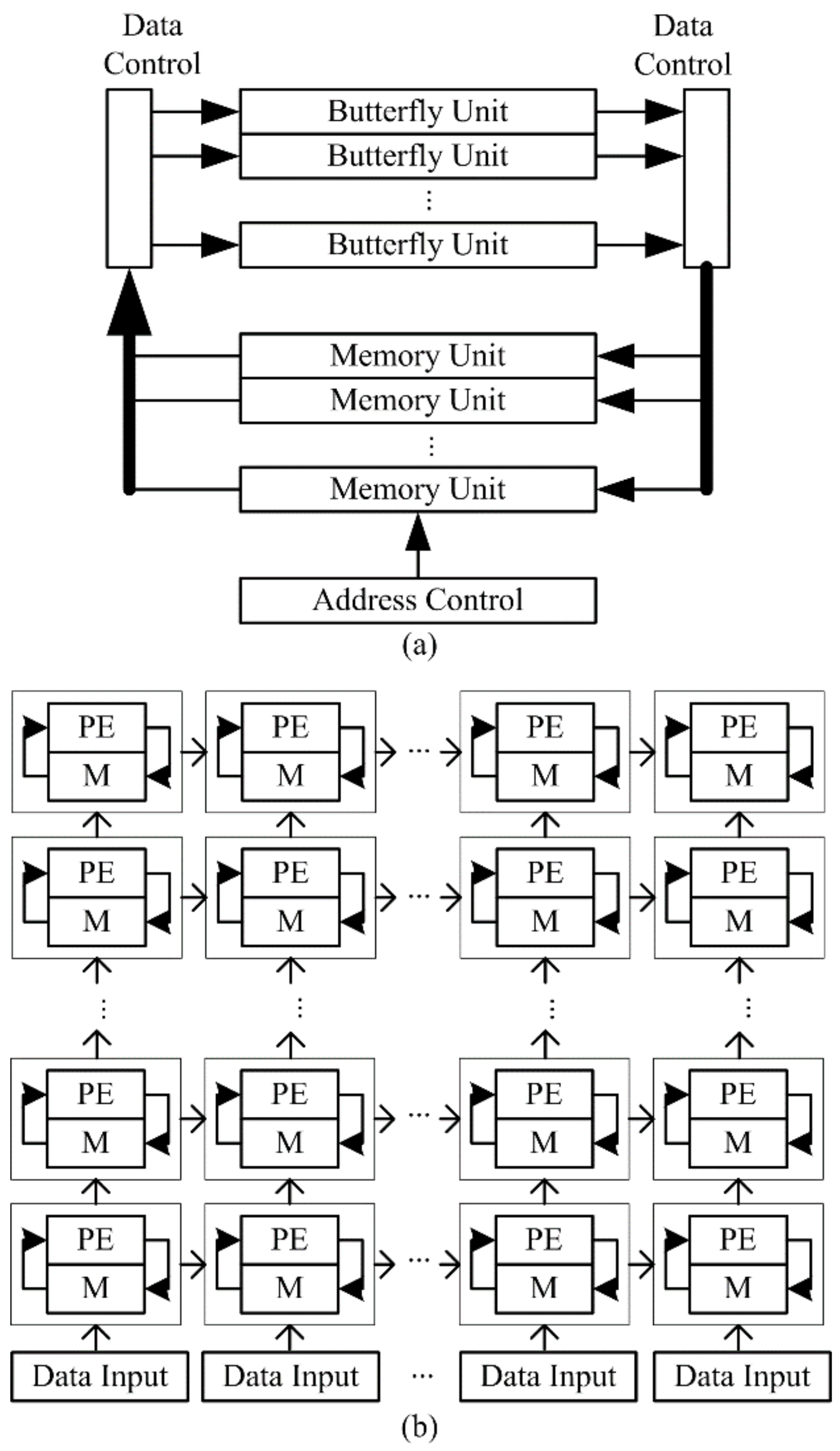
36] (
Figure 1a), where small circuit size is typically a priority, and as a result the number of clock cycles required to complete an FFT is much greater than
N. Next is a traditional pipelined FFT based on a single-path radix-2
2 delay-feedback (SDF) architecture from Intel [
37]. Like most pipelined FFTs,
N clock cycles are required to perform an
N-point transform. Finally, at the other end of the spectrum, by adding parallelism based on multi-path delay commutator (MDC) and SDF stages, a circuit architecture that computes the FFT in much less than
N [
4] clock cycles is included. All the circuits allow run-time choice of 128/256/512/1024/2048-point transform sizes, except for [
36] which also offers 16/32/64-points and [
4] which does all but 128-points, but does offer a multi-mode capability for processing some transform sizes in parallel.
In
Table 4, three of the designs (DMBA, Intel, [
4]) used the same Stratix IV EP4SGX530KH40C3 FPGA (−3 speed grade). The other design used a 5SGSMD5K2F40C2 Stratix V FPGA (28 nm technology). Since the Stratix V FPGA uses a more advanced architecture, is based on better CMOS technology, and is the fastest −2 speed-grade, the results for [
36] in
Table 4 could potentially yield better results.
It is important to note in
Table 4 that the DMBA Fmax of 490 MHz is limited not by the FPGA fabric, but is a result of the maximum operating speed of the simple dual port embedded RAMs used. The TimeQuest generated DMBA Fmax associated with the LUT/register fabric is >500 MHz. Note that the DMBA FFT circuit operation at 500 MHz was verified using a development board based on an Intel Stratix III EP3SL150F1152C2 FPGA.
The memory-based design [
36] is a 16-bit radix-2 FFT with two butterfly units and uses a 16-bit twiddle factor. The tradeoffs show that although this memory-based design uses 6.1/4.0 times fewer LUTs/registers than the DMBA, it runs 13.6 times slower, even using a faster FPGA speed grade and technology.
For the Intel 16-bit pipelined FFT (IPv17.1), the values in
Table 4 show that the Intel circuit uses 27%/38% more ALMs/registers, but the DMBA uses 29% more LUTs; however, the higher DMBA throughput leads to a better throughput per logic cell by 87% (2048-points), even with the RAM speed restriction. This Intel FFT is slower than Intel’s fixed-point FFT (
Section 6.2) because the 16-bit input word length grows to 28-bits at the output, which was done to keep SQNR high. Processing these longer word lengths and likely larger multipliers slows down the Intel SDF speed. It should be noted as well that for the Intel circuit any post-processing, such as that needed for common operations such as convolutions, would require 28-bit circuitry rather than the 16-bit DMBA word-length, thus nearly doubling the resource usage. Finally, the DMBA FFT has been successfully programmed and tested to support cyclic prefix generation and insertion needed for the targeted LTE protocols, whereas the Intel circuit would require a separate 28-bit circuit to perform this function.
The last circuit in
Table 4 [
4] is a parallel pipelined FFT circuit based on radix-2 MDC and radix-2
4 SDF stages, all of which have 8 I/O ports. Data output is not in natural order, so a reordering circuit would be necessary to make this design closely comparable. The parallel operation provides processing of eight complex samples per clock and reduces overall latency, but the added circuit complexity results in 11.4/6.7 times more LUTs/registers, yet achieves an FFT throughput time that is only 83% faster than the DMBA. Although the latency (first point in to first point out) in clock cycles (299 for 2048-points) is 11.7 times less than that of the DMBA (3507 clock cycles for 2048-points), the latency in time is 2.69 µs vs. 7.16 µs for the DMBA, an improvement of only 2.7-fold. With a reordering output buffer, the improvement would be reduced by approximately two-fold [
4].
6.5. Non-Power-of-Two Circuit (LTE)
6.5.1. Introduction
SC-FDMA is a part of the LTE protocol [
3] used for up-link data transmission. It involves a DFT pre-coding of the transmitted signal, where the DFT can be any one of 35 transform sizes from 12-points to 1296-points, with
N = 2
a3
b5
c and
a,
b,
c positive integers. The rationale for targeting FPGAs is due to the rapidly growing FPGA use in communications applications, e.g., base stations and remote radio heads at the top of cell phone towers. Here, we provide results of mapping the DMBA to Xilinx Virtex-6 devices.
6.5.2. Related Work
To compute high performance run-time transforms for
N ≠ 2
n, a variety of mixed radix approaches have been proposed [
38,
39,
40,
41]. The performance of the different designs is primarily related to the complexity of the butterfly unit design.
Both Xilinx [
41] and Intel [
38] use a memory-based architecture as in
Figure 1a, consisting of a single multi-port memory that sends/receives data to/from a single arithmetic unit that performs the required butterfly computations. For these designs, the number of clock cycles per DFT is greater than the transform size
N, so it is not possible to continuously stream data into and out of the circuit. In the Xilinx design, the arithmetic unit can do radix 2, 3, and five-point butterflies using parallel and pipelined hardware. It can perform two radix-2 operations per clock cycle, one radix-3 or radix-4 operation per cycle and one radix-5 operation in two clock cycles. The Intel design uses a simpler butterfly unit which results in lower performance, but also reduced LUT/register usage.
The other designs are different from those discussed above in that they either use a higher radix memory-based design [
39] or a pipelined architecture [
40] to reduce the overall number of cycles needed to compute a DFT to less than the actual transform size
N.
6.5.3. DMBA Design Approach
Although the value of
N can be obtained with just radices 2, 3 and 5, the architecture chosen here is based on a value of
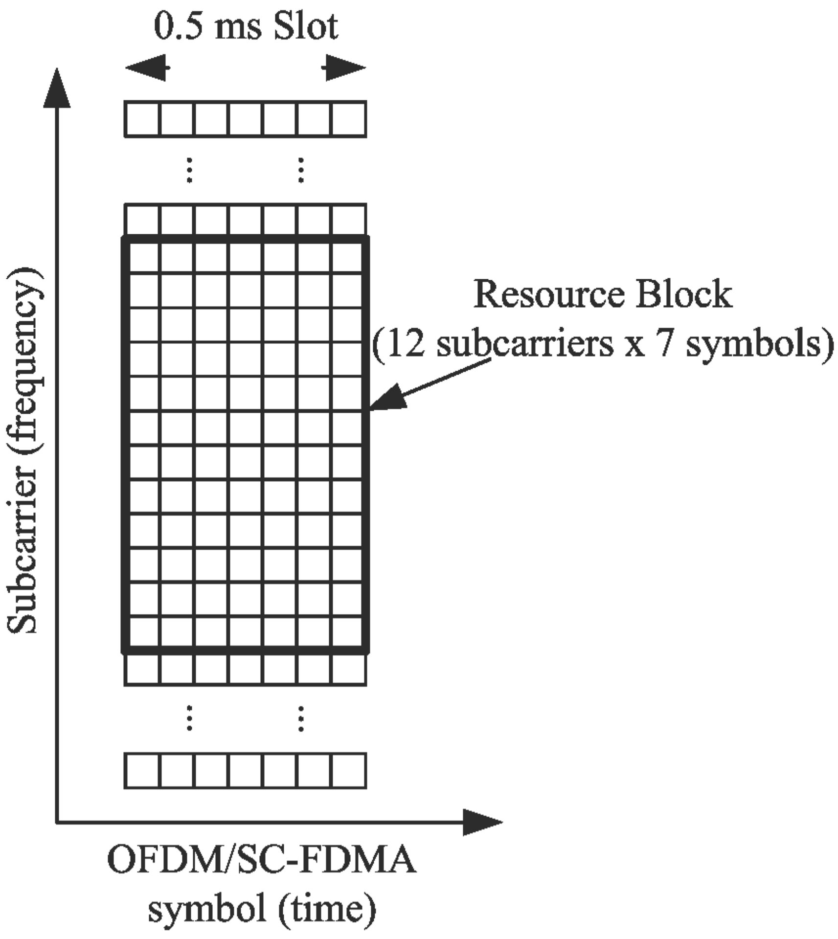
b = 6, so that radix-6 is an option. This value was selected because all SC-FDMA DFT sizes include a factor of 6, since a LTE resource block (RB) or the smallest group of subcarriers used by the SC-FDMA protocol (
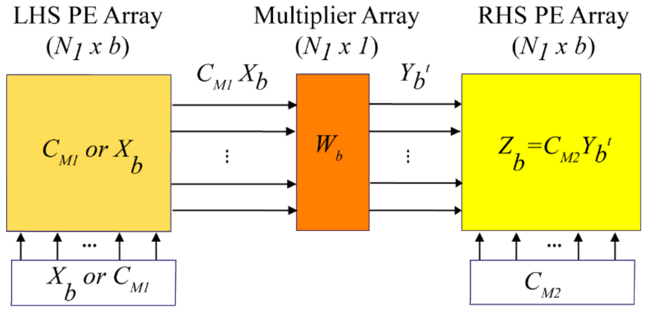
Figure 10) has at least 12 subcarriers. Therefore, using a radix-6 option translates to more efficient processing for all 35 sizes. The actual structure of the architecture is then that of
Figure 5 with
b = 6. This choice means that the array also contains sub-set
b ×
b arrays with
b = 2, 3, 4 and 5, so base-2, 3, 4, and 5 processing can also be performed.
A physical array structure with
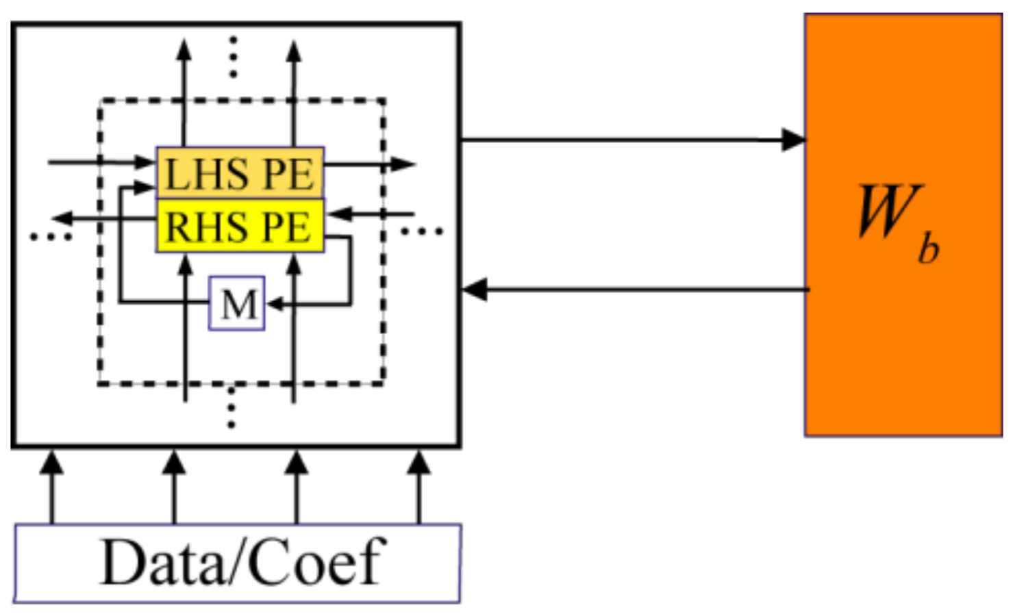
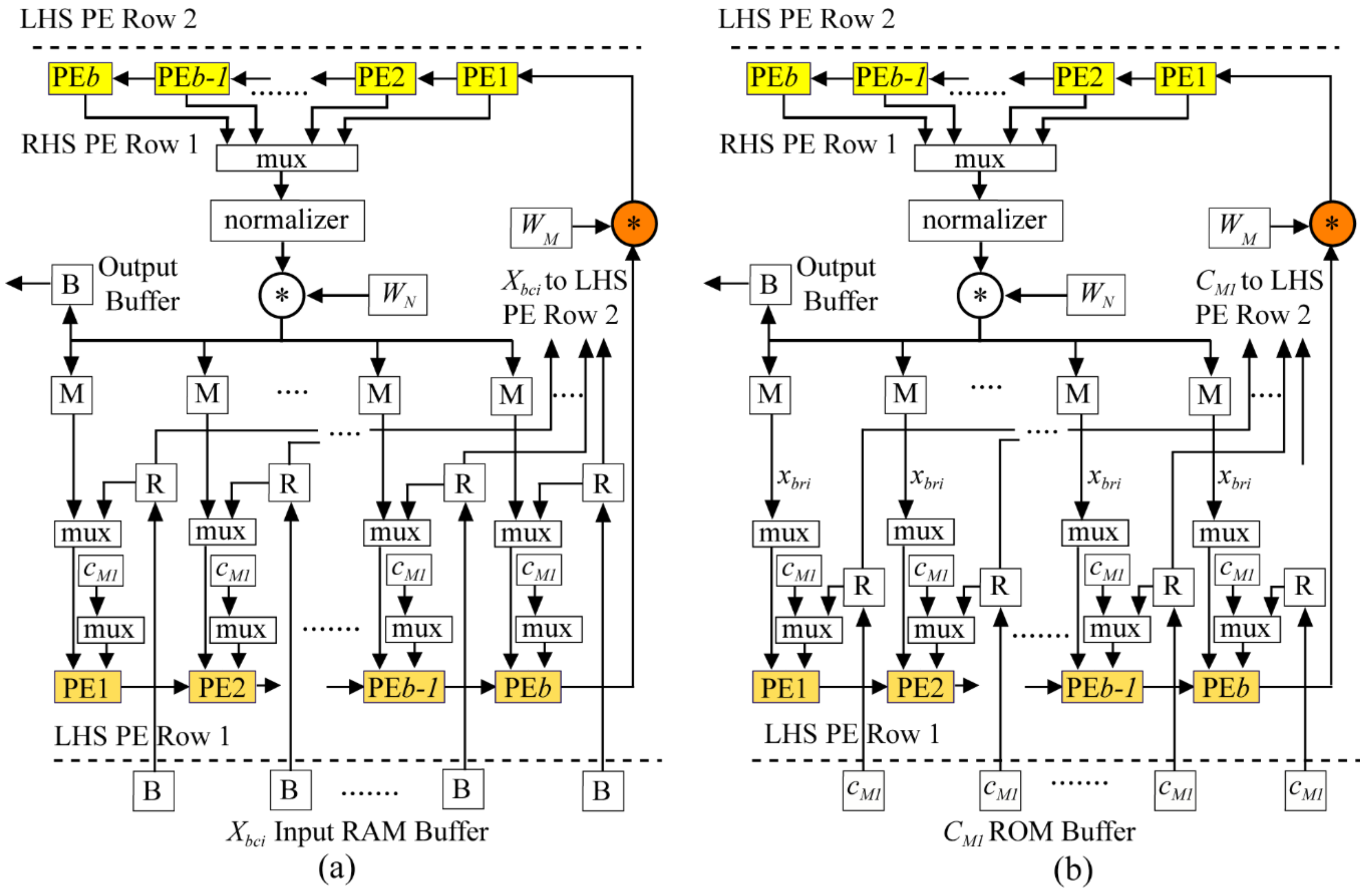
b = 6 would result in higher throughputs than needed for SC-FDMA applications. Consequently, the physical array consists of only one of the PE rows in
Figure 8. In other words, each virtual LHS, RHS, and multiplier PE column in the array is projected (collapsed vertically) onto a single PE row. Thus, there are six RAM memories associated with the six LHS/RHS combination PEs. This linear array emulates the operations of the 2-D
b ×
b virtual array of
Figure 5, but completes a DFT computation a factor of six times slower.
6.5.4. On-the-Fly-Twiddle Coefficient Calculation
Since the goal of this design was to provide a run-time option to compute any number of transform sizes, the number of twiddle coefficients that would need to be stored could be unbounded. The total number of twiddle values needed for LTE SC-FDMA itself is about 6500 words. There are schemes for reducing twiddle factor storage to as little as
N/8 based on sin/cos symmetries [
35], but these are only useful for power-of-two based FFTs.
For this reason, an approach based on a programmable on-the-fly-generation of the twiddle values for a DFT size has been adopted. This twiddle coefficient engine uses a single complex multiplier, a table of twiddle seed values, and a set of size parameters as a basis for doing this. The iterative equation , where and is a seed value, is used to generate values for a particular DFT size given the starting seed.
It would be possible to generate the N twiddle values for a transform size with a single seed value, however there is more circuit complexity involved in doing this because the twiddle factors must be generated in a special order due to the algorithms used. Additionally, there are numerical considerations that come into play as well. A better tradeoff was to use a separate seed for each column of a twiddle matrix. For example, if a 960-point DFT is factored as 30 × 32, 32 seed values would be needed to generate all twiddles.
In the implementation of the LTE SC-FDMA, the twiddle generation circuit required only 937 words of memory to hold all twiddle seeds needed for 35 DFT sizes. The logic needed to implement the entire programmable twiddle circuit was only about 10% of the circuit hardware.
6.5.5. Programmability
The base-6 circuit described here was programmed at a more abstract level than the base-4 circuits in
Section 6.2,
Section 6.3 and
Section 6.4. It used a single RAM memory to hold parameters that determine the specific factorizations and execution orderings used for loop index ranges in the Verilog coded control modules.
To illustrate the programmed data flow, consider the example
N = 540
= N3 ×
N4. Since our implementation consists of 6 × 6 SAs, it would be most efficient to choose the factorization
N3N4 = 36 × 15 = 6
2 × (3 × 5) because this makes best use of all the hardware. In this case, the processing consists of 15 36-point column DFTs followed by 36 15-point row DFTs. The input
Xb is stored in the input buffers in such a way that it is accessible as a sequence of blocks
Xbci,
i = 1, …, 15 of 6 × 6 column data. Then, the 36-point column DFTs are done using (3) with
M = N3 = 36
= N1ciN2 = 6 × 6,
(
b = 6) and
,
i = 0, 1, …,
b − 1;
k = 0, 1, …,
b − 1. Each
Xbci enters the array at the bottom of the LHS SA (
Figure 5 and
Figure 8) and flows upward with systolic matrix–matrix multiplications performed as before. As each of these 36-point column DFTs are computed, they are multiplied by elements in the 36 × 15 twiddle matrix
W520 which are generated on-the-fly. During this processing, all PEs are used with 100% efficiency.
After twiddle multiplication by
W540, the multiplexor in
Figure 8a is used to store data for the 15-point row DFTs in a way that they can be accessed as 3 × 5 data input blocks,
Xbri,
i = 1, …, 36, from the internal PE RAMs. Each of the six PE virtual rows is responsible for storing six DFT matrix rows as six 3 × 5 blocks in associated internal RAMs.
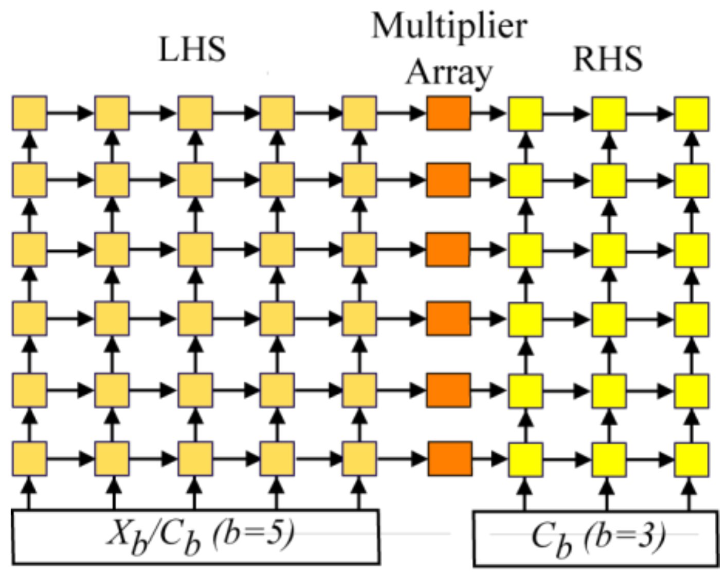
For the row DFTs, not all the LHS/RHS PEs are used. Rather, as shown in
Figure 4, the LHS side SA reads from RAMs in five of the six PE columns to do the five-point transforms by multiplication of these data blocks by
C5 values fed from the bottom of the LHS array. The multiplier array then multiplies these transform values arriving from the LHS array by appropriate elements of a 3 × 5 twiddle matrix stored in a small ROM. Finally, only three PE columns are used on the RHS array to perform all the three-point transforms. Results are stored in an output buffer and are output in normal order.
The control hardware is aware of the number of rows/columns used in the LHS and RHS arrays during the computations, the different coefficient and twiddle matrices required, the read/write memory addresses, the sequencing in/out of data storage and retrieval patterns, etc. All this parameter information is saved essentially as a table in the ROM memory. The programmability arises because when a DFT size is requested, the corresponding table is read from ROM and used to set loop values in the Verilog control code. The number of different DFT sizes that can be supported is then only limited by the size of this parameter memory.
It is important to note that the same architecture can be programmed to perform power-of-two FFTs as well. This is important, as almost all wireless protocols—including LTE—require power-of-two computations and having both options available in the same circuit could be useful for future wireless applications.
6.5.6. DMBA LTE SC-FDMA Transform Throughput and Latency
Table 8 shows, for each SC-FDMA transform size
N, the corresponding throughputs (
T) and latencies (
L) in clock cycles for the design. In this context, latency is defined as the number of clock cycles it takes to finish the first transform in a series of transforms. The DMBA FFT cycle counts are based on Modelsim Verilog simulations. Note that for the smaller transform sizes, 12-, 24-, and 36-points, the circuit supports constant streaming of the data into and out of the circuit.
6.5.7. Comparison with Commercial Circuits
In this section, the proposed LTE SC-FDMA DMBA is compared to Xilinx and Intel versions of the same circuit. To provide a more relevant metric than throughput and latency numbers, we calculated the length of time necessary to compute an LTE RB, as shown diagrammatically in
Figure 10. For example, 1296 subcarriers would imply processing a maximum of 108 resource blocks. This is a good performance comparison metric in that it requires both low latency and high throughput.
A Vertix-6 (XC6VLX75T-3ff7484) FPGA was used as the target hardware for both the Xilinx and the DMBA. The Xilinx LogiCORE IP version 3.1 was used to generate a 16-bit version of their DFT because the SQNR of 60.0 db (mean over all 35 transform sizes) was comparable to the DMBA 12-bit circuit with mean SQNR = 63.3. Xilinx LogiCORE includes a bit accurate C model, callable as a Matlab mex function, that was used to obtain Xilinx SQNR values.
The resource comparisons in
Table 9 use a block RAM normalized to 18-kbits, so that a Xilinx 36-kbit block RAM is considered equal to two 18-kbit RAMs. Also, the “RB Avg” column provides the average number of cycles (over all 35 DFT sizes) it takes to compute the DFT for the seven symbols defined by a RB as a function of the transform size
N. Finally, the Fmax value (here Fmax is not the sample rate) and the number of RB cycles are combined, providing a measure of the throughput, which was normalized to 1 in our design (higher is better).
Table 9 shows that Xilinx LUT usage is higher by 32%, register usage by 68%, average computational cycles by 41% while normalized throughput is 39% higher for the DMBA. Consequently, the overall combined gain is significant.
In terms of throughput in clock cycles, the Xilinx average over 35 DFT sizes was 3.3N, whereas that for the DMBA was only 2.1N. If these numbers are used as a measurement basis to calculate throughput per logic cell (7), then the DMBA efficiency is 130% higher.
The 401 MHz Fmax clock speed is lower than the other DMBA Fmax values in earlier examples because the critical path here is in the control hardware rather than the array structure itself. Additional control-level pipelining would be necessary to move the critical path out of the control hardware.
Unlike Xilinx, Intel does not offer a DFT LTE core; however, they have published results of an example design running on a Stratix III FPGA that provides a useful basis for comparison. This design example is different compared to the DMBA here in that it does not offer a 1296-point transform option and the outputs are not in normal order. Adding buffer circuitry to sort the output data would require additional logic and add ~
N additional words of memory (~5 Stratix III M9K RAM blocks) to the numbers shown in
Table 9.
For comparison, the DMBA was also targeted to a Stratix III FPGA (EP3SE110F780C2). The Intel implementation uses less logic but is far slower, both in terms of the lower values of Fmax and the increased number of cycles to complete the RB computation. Consequently, the DMBA design had about three times higher throughput while LUT usage was only ~47% higher (some of this could be due to a lower speed grade used in the Intel design—this was not specified). It should be noted that the Intel latencies would be relatively understated given that data output is not in normal order.
The DMBA FFT circuit operation at 450 MHz was demonstrated on an Intel Stratix III EP3SL150F1152C2 FPGA using a development board.
6.5.8. Other FPGA LTE Implementations
The other two designs are different from those in
Table 9 in that they use a higher radix [
39] or a pipelined FFT [
40] (single-path delay feedback) architecture to reduce the overall number of cycles needed to compute a DFT in less than the actual transform size
N. This means it is possible to have a streaming architecture, e.g., one where data flows continuously into and out of the circuit (Fmax is the same as the sample rate).
No SQNR data was supplied to indicate the circuit precision, although the internal precision in [
39] was 18-bits and [
40] used a mixed floating point (the same exponent for real and imaginary words) and block floating point. Details regarding latency are not discussed in these papers; however, comparison is still instructive and performance can be estimated based on throughput alone, which is more important than latency for computing resource blocks.
The comparison results for Virtex FPGAs are shown in
Table 10. For the DMBA, the average throughput as a function of
N for all 35 transform sizes is 2.1
N, which is a factor of two higher than the other implementations. However, these more complex architectures require far more LUT hardware, 2.7 times and 3.7 times for [
39] and [
40], respectively. Although [
40] uses fewer registers, this is less meaningful because the 10:1 ratio of LUTs:registers in FPGA hardware leads to imbalances that can cause many registers to be inaccessible. Additionally, using a normalized throughput like that in
Table 9, the DMBA could be correspondingly faster by perhaps 56% for [
39] and 3-fold for [
40]. FPGA details would be needed for an accurate clock speed comparison.
