1. Introduction
The ever-increasing computational requirements in modern digital signal processing force the systems to obtain higher processing capacity and higher throughput simultaneously. Various architecture alternatives are capable of performing these tasks.
Due to their high volume, powerful general purpose processors are a straightforward way to accelerate digital signal processing, but such processors must consume a large fraction of transistors to flexibly support diverse application domains, thus can often be inefficient for specific workloads. On the other hand, in the era of diminishing returns from technology scaling, fixed power budgets and the end of Dennard scaling [
1,
2] have led researchers to embrace accelerators in order to sustain performance and energy efficiency increases. Hardware acceleration is widely used to gain performance, power and energy improvements. Accelerators are often designed as standalone IP blocks that communicate with the rest of the system. In the field of accelerators, there are two broad categories: Field programmable gate arrays (FPGAs) and application specific integrated circuits (ASICs).
FPGAs use elementary components—lookup tables—as building blocks and glue them with a flexible interconnection network, combining the benefit of spatial execution with programmability. They compete with their ample logic resources but suffer from low operation frequency and low logic utilization rate, and thus limit the performance in the delay, area, power consumption, and reconfigure time. Such solutions cannot implement coarse-level operation efficiently and are not suitable for systems with the strict area and frequency constraints. The other class of customized accelerators, implemented as ASICs demonstrated substantial advantages in performance and power over the instruction driven general-purpose processors, and they can perform key kernel computations to achieve orders of magnitude of improvements in performance and energy efficiency. They are now integral components in modern SoCs, powering a variety of applications like video codec [
3], data processing [
4,
5], and deep learning [
6].
There have been some successful accelerators that manage to implement dedicated hardware to accelerate commonly used digital signal algorithms, like kernels as a high throughput matrix multiplication accelerator [
7] and an FFT accelerator implemented in FPGA [
8], or applications as a high performance and energy-efficient H.264 encoding [
9] and a machine learning accelerator accommodates seven representative techniques [
10]. In such cases, they can only apply to one specific application, when a task involves a series of applications, the system may need multiple accelerators to obtain desired performance, or when the target algorithm shifts from, for example, FFT to matrix inversion, such accelerators might easily become useless.
Most modern devices run several important tasks, and therefore multiple accelerators will be required, and this could mean that although each accelerator is area-efficient, a combination of accelerators might not be. Furthermore, multi-accelerators will inevitably induce extra communication congestion, thus reducing the overall throughput rate [
11].
We find out that in most of the multiple accelerator systems, each accelerator’s computation resource and its local scratchpad is only visible to its own datapath [
12]; in order to avoid the high resource cost and memory cost, we build a configurable accelerator system that includes multiple algorithms that take the utility of spatial computing resources and shared on-chip memory [
13]. The benefits are that it improves the utilization of computing resources and eliminates explicit data copy between accelerators.
For the targeted workload domain, we build a heterogeneous processing element (PE) array consisting of different functional units, with 32-bits data width and a 64-bits scratchpad width owing to the single precision complex floating-point number operation.
In particular, this paper makes the following contributions:
- (1)
Shows the details of how to build a PE by exploiting the spatial parallelism of kernels. Based on these PEs, multiple kernels can be implemented through hardwired algorithm controllers. Furthermore, complex tasks can be accomplished through the combination of algorithms.
- (2)
Detailed analysis and experiments are carried out to demonstrate the performance advantage of RASP, and the additional performance enhancement by adopting a multi-port shared local scratchpad is shown with experimental proof.
- (3)
To alleviate the programming effort, we present a convenient method to organize these independent algorithms, in the proposed approach, the compiler and conventional programming are largely eschewed due to the parameters used for configuration are highly abstract. These parameters are exposed to the programmer via a programming library [
14].
Organization of the paper in the rest of the sections is as follows: system overview, workload analysis, and the basic compilation workflow are described in
Section 2. The critical factors of an accelerator system and the acceleration analysis of the proposed system are explained in
Section 3.
Section 4 introduces a real-life test case execution process. The results analysis is given in
Section 5. Finally, a conclusion of the paper is presented in the last section.
2. System Design and Workflow
In this section, we will give a brief description of the proposed system’s microarchitecture and its compilation workflow, including some primary design considerations like workload characterization and acceleration kernels selection.
2.1. System Architecture Overview
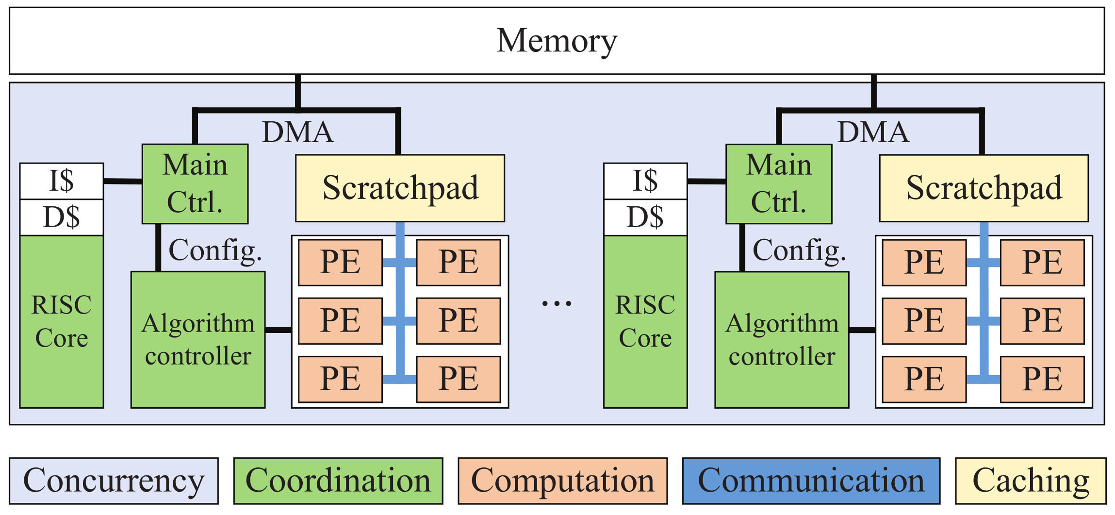
The proposed system is a heterogeneous digital signal processor built around two primary entities, a low-power core, and an accelerator engine. We use the low-power core to coordinate the system and the accelerator while retaining programmability for the serial part in an application that is not suited for acceleration. The low-power cores act as system supervisors, running operating systems and managing the initialization and configuration of the accelerators. The acceleration engine of the system is a configurable domain-specific accelerator that aimed at high precision and high throughput radar digital signal processing.
Like most of the standalone accelerators [
15,
16,
17], the accelerator in the proposed system–called reconfigurable application specified processor (RASP), is a loosely coupled configurable engine attached to the AXI bus. Data communication between on-chip memory and external storage, i.e., DDR3 is provided through direct memory access (DMA) in the RASP. Configuration bit streams are generated by compiling customized application programming interface (API) functions and specific address space in external DDR is allocated to store them. With the help of API functions, programmers only need to define a set of parameters to build a task, without too much worry about hardware implementation and restriction.
Figure 1 shows the high-level design; each engine consists of a PE array and scratchpad, connected with the memory via DMA. It is initialized by a RISC core, which compiles and sends commands to the main controller in RASP. Inside each accelerator, we use main controller for processing scheduling and algorithm controller for kernels execution.
2.2. Workload Analysis
A workload is considered as a pool of applications, part of an application can also be partitioned into several computing kernels.
The proposed system is geared primarily toward high-performance radar digital signal processing, where autocorrelation can give information about repeating events and estimate mean value uncertainties, and cross-correlation is useful for determining the time delay between two signals. To increase the range resolution and the signal to noise ratio, we use pulse compression, to reject clutter echoes and detect targets, and we can use moving target indication (MTI) or moving target detection (MTD). All the applications mentioned above can decompose into a single or a series of serializable kernels.
Among these kernels, we found that a significant amount of vector and matrix operation are exposed. This requires the engine that can fulfill both basic linear algebra subprograms (BLAS) and complex computing kernels like FFT, FIR, and matrix inversion, as well as some basic mathematical libraries such as division and trigonometric functions. Based on these subroutines, various applications can be performed.
Fortunately, as alluded to in the article that typically accelerated workloads in a domain have common characteristics [
9,
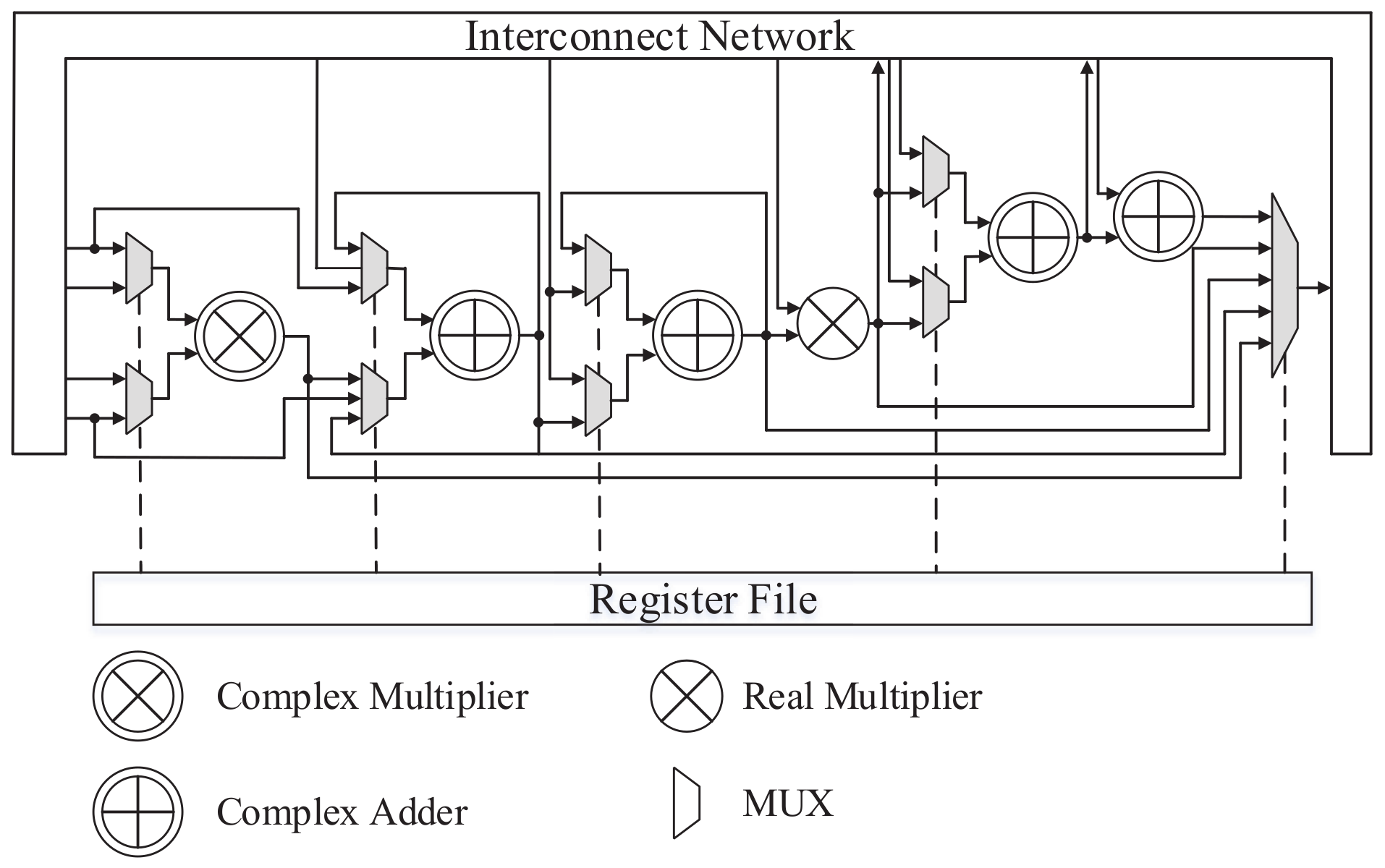
18], the main computation patterns in the radar processing sub-algorithms include convolution-like data-flow computation patterns, butterfly-unit, multiply-accumulate, simple vector multiplication, and vector addition. These patterns have the high computational intensity and long phase with simple control flow. In the design case, we enumerate the computation patterns and build a problem-specific PE that can cover all the patterns. Specifically, in the PE array, four of them are homogeneous, and each consists of a complex multiplier, four complex adders, and two real multipliers; two of them are heterogeneous to process operations like division, transcendental function, and fixed to floating-point conversion. The micro-architecture of the homogeneous processing element is shown in
Figure 2. In order to fully explore the performance of computation patterns mentioned above, we adopt the irregular structure. Compared with regularized micro-architectures in traditional processors, which depend heavily on the complex pipeline configuration and task compiler technology, the irregular structure only aimed for finite computation patterns in radar signal processing, so the efficiency of the computation resource and the performance of parallel pipelining can be improved. The register file stores the information that configures the PE function, and the intra-PE data communication is achieved via the interconnect network.
Each sub-algorithm has a corresponding hardwired controller, and these controllers can create datapaths that are tightly connected to processing elements and data storage elements. The algorithm controllers assign the register files attached to the processing elements directly to provide opcodes for the above-mentioned computation patterns. By deploying customized datapath and control for these specific algorithms and applications, impressive performance and energy advantages can be achieved [
19].
The details of representative kernel implementations have been reported in previous publications, include FFT [
20] and matrix inversion [
21].
Theoretically, the proposed architecture can fulfill all tasks composed of these kernels efficiently; this characterization is both its major strength and a limitation, by exploiting the efficiency of a customized datapath and the convenient combination of kernels, complex tasks can be achieved efficiently. However when a task involves a kernel that is outside of the coverage, we need to offload the unaccelerated part to the general processor, and this process may introduce additional control and communication overhead.
In principle, for a large part of aimed applications, the system is required to process data streams under real-time constraints and obtain the prescribed throughput.
2.3. Compilation Workflow
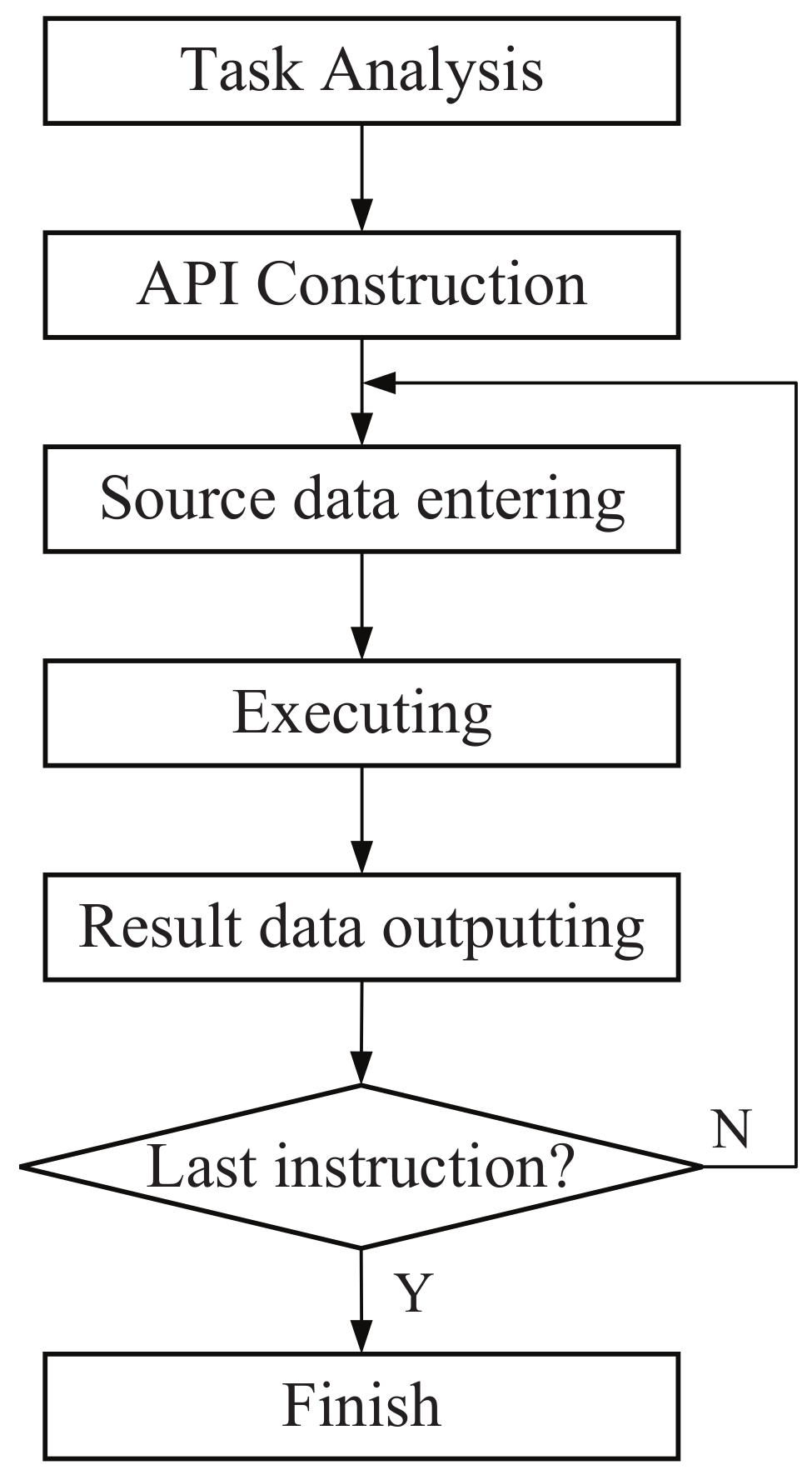
Cooperating with the algorithm controllers, through highly abstracted parameters configuration, i.e., the type of algorithm, size of the algorithm, source data address, destination data address, and so on, RASP can execute independently without additional intervention once these parameters are configured to the main controller. As a result, the complexity of invoking a task is significantly reduced.
From a programming point of view, the whole workflow consists of a series of steps by orchestrating the process of synchronization, engine activation, address assignment and execution of computation kernels performed by the accelerator engines. In the execution phase, the computation and data transmission are independent steps and are controlled by different hardware components in the main controller, respectively. For small size algorithms that source data that can be stored entirely in the local memory, the system transfers the data first and then performs the computation. When the amount of data exceeds the storage space, the system can perform a ping-pong operation, with half of the memory space for computation and the other for data transmission. Decoupling the memory access from the computing process also helps to ease the procedure of task execution.
The main processor (general processor) configures the work mode of the RASP and generates configuration information for the algorithm execution. Here are the details for the compilation process for algorithm execution: the input application is described in a high-level language. Firstly, the code is programmed manually with the collaboration of calling API function, then compiled by the host processor, generating a string of bit streams written to external memory, and these bit streams are the initial configuration information that will be sent to RASP. RASP can receive this initial configuration information directly from a host processor or fetch them from external memory initiatively, and the main controller accepts and translates them. The translation results determine which sub-algorithm is to be executed, what size the sub-algorithm is, and so on.
When dealing with a new task, the first step is to go through a rough analysis of the contained kernels and the corresponding size range. Application partitioning is performed at compilation time and driven by dedicated API functions. All of the supported kernels have a corresponding API for function construction. After decomposing the task into a set of sub-algorithms, the next step is to construct the compilation function by the API calling.
The application execution flow is shown below in
Figure 3. After the compiled bit stream is configured to the main controller in RASP and the data are offloaded to scratchpad memory, the execution begins. After completing a single kernel, the result data are ready to be sent out to the external memory.
Such a high efficiency and convenience programming workflow can open up the usage of RASP in a broad set of systems and for a broad set of applications.
With the rich computing resources, a primary goal of application allocation is to exploit the data bandwidth and resource utilization rate. The analysis will be carried out in the next section.
3. Acceleration in Application Level
Combined with a simplified performance model for hardware accelerators, we analyse some strategies used in the system and the speedup of some representative algorithms.
3.1. Accelerator Gain Analysis
From the reference [
22], we can conclude that in the loosely coupled systems, the offload time is usually fixed and granularity independent, but the transmission latency is strongly granularity dependent. To obtain higher performance gain, the natural solution is to reduce the latency and increase the accelerator factor.
3.2. Data Interface Latency Analysis
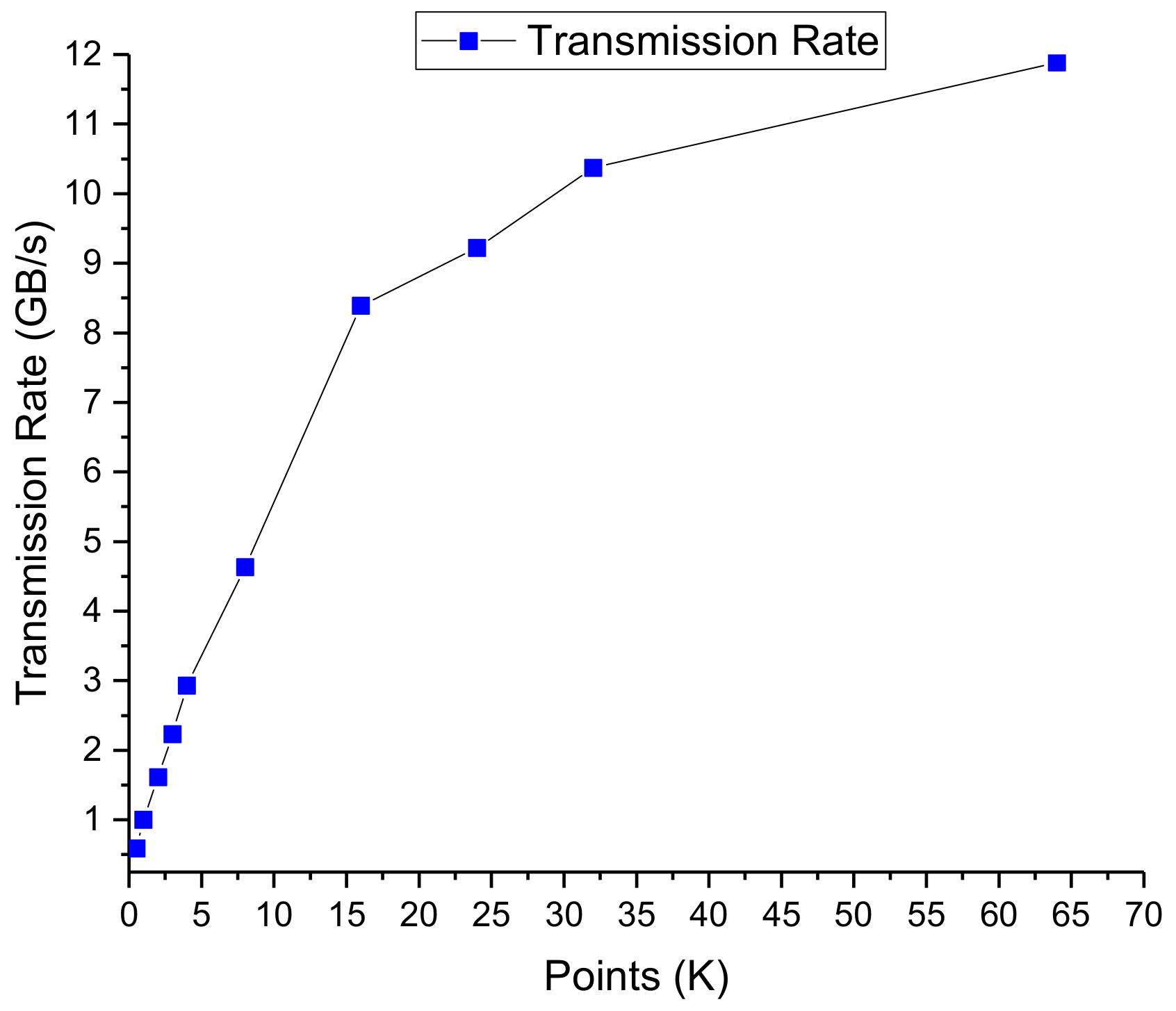
Figure 4 shows the transmission rate of different data size range from 0.5 KByte to 64 KByte of RASP. The values are collected by real chip test rather than simulation model test, so the data has great reference value. It’s clear that due to the overhead of setting up a transaction, the transmission efficiency is very low when the data amount is small [
23], and is gradually trending to saturation as the amount of data is getting bigger. This is because the overheads of setting up a transaction are usually amortized over a large bulk transfer.
Under such circumstance, and according to the above analysis about accelerator execution time breakdown, to achieve higher efficiency, it is natural that we should avoid small chunks transmission via DMA to the greatest extent. Therefore, we use a large addressable on-chip memory to store the result data of the algorithms, which serves as the source data of the following kernel in the task.
3.3. Algorithm Speedup Ratio
To achieve high efficiency, a key advantage of the loosely coupled accelerator is that it can unleash the parallelism inherent in the kernels they accelerate by instantiating tailored many-ported memories and more functional units, especially in the accelerators that leverage DMA for data transmission and scratchpad for data storage.
The multi-bank partition also enables multi-channel parallel. Specifying more memory banks and more functional units yield better performance with increased power costs [
24], but take the data transmission bandwidth restraint into account, additional partitioning becomes wasteful for there is no enough bandwidth to feed data efficiently. In the proposed accelerator, we use six PEs, and four of them have the same structure to complete a four-channel parallel operation and we divide the scratchpad into 32 banks, with the total size of 2 MByte.
The main consideration of using four homogeneous PEs is the data supply capability. The data to be processed in the system are single-precision complex floating-point numbers and four PEs (4 × 64 bits) match the AXI data width. On the other hand, the computation time should be equivalent to data transmission time. For example, in FFT, it takes eight cycles to process a complex number, and this data processing rate matches the data transmission rate. Therefore, it is a balance between computing power and data supply capability. The reason for using 32 banks has a direct correlation with the number of PEs. With four PEs, most of the algorithms can perform 4-channel parallel; in the maximum case (FFT and matrix inversion) we need eight ports for source data and eight ports for result data. Taking the double buffering into consideration, 32 banks just meet the requirement.
For performance evaluation of the proposed RASP, the computation cycles obtained from chip testing are compared to that of a TI DSP [
25]. The chosen comparative product is a state-of-the-art multicore high-performance fixed and floating point DSP that featured applications such as avionics and defense, high-performance computing, software-defined radar and so on, and the DSP benefits from the superset of C67x+ and C64x+ ISA, which are optimized for mathematical operations and digital signal processing. RASP and the contrastive DSP has the same amount of floating-point multipliers.
Figure 5 shows the average speedup of RASP over TMS320C6672 when executing a series of representative algorithms. The Level 2 BLAS contain vector operations and the Level 3 BLAS are matrix operations like general matrix multiplication (GEMM) and matrix covariance.
Even though the TI DSP can benefit from the superset of C67x+ and C64x+ ISA that is optimized for mathematical operations and digital signal processing, DSP is an essentially sequential processor that contains instruction fetch, instruction decode, execution and so on. However, the RASP can benefit from the dedicated datapath and communication. For these reasons, the RASP can achieve performance speedup of 1.9×–10.1× for different algorithms as indicated in
Figure 5.
We can notice that matrix inversion has much higher speedup than the other algorithms; this is because matrix inversion is more complex compared with matrix multiplication or FFT; it contains multiple steps so the support of ISAs may be not as good as the other algorithms, and meanwhile, the RASP has made special optimization for matrix inversion.
3.4. Comprehensive Analysis
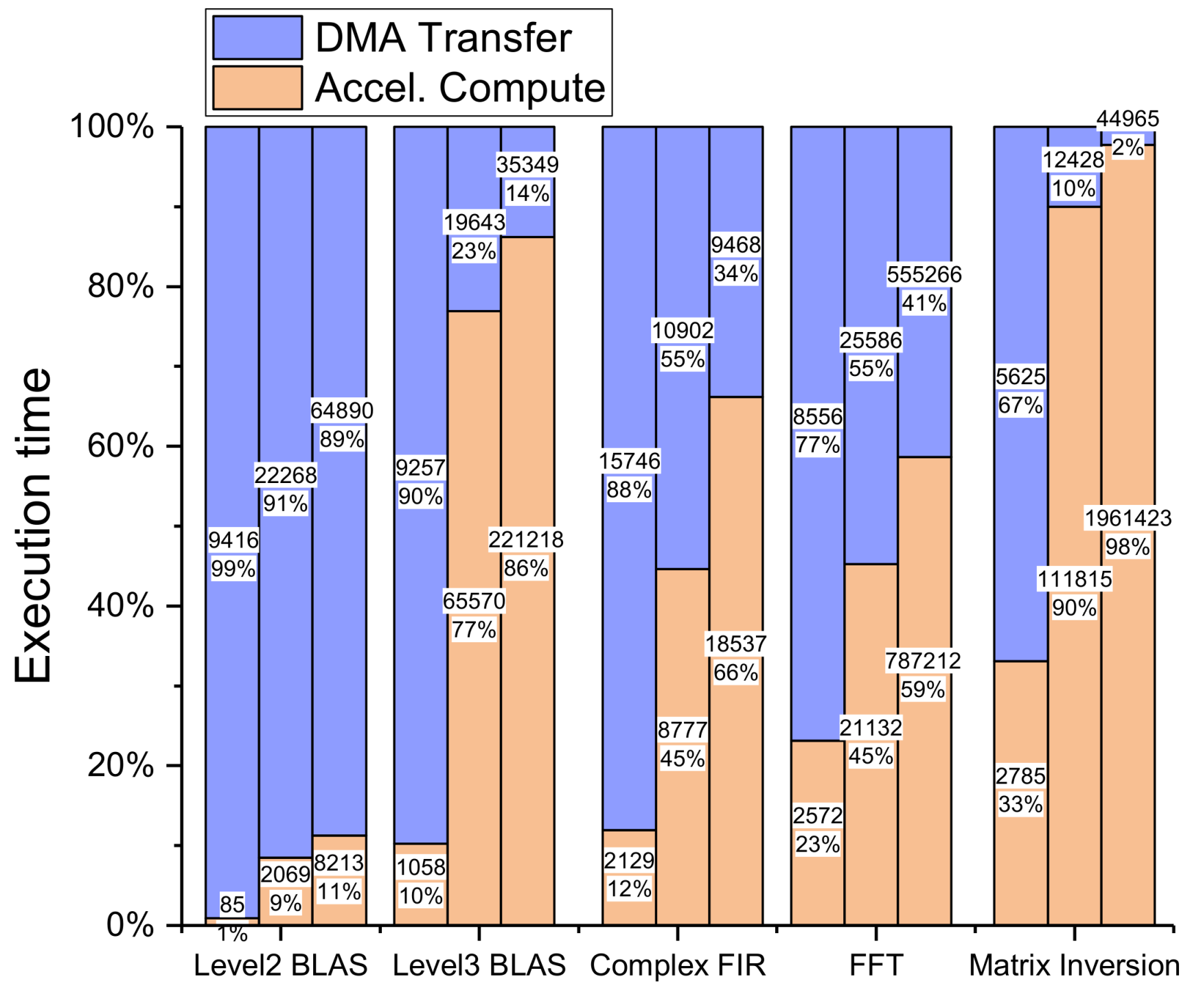
To illustrate the importance of data transmission on the efficiency of the entire application execution, we go through an analysis of different types of kernels about the ratio of data transmission and accelerator computation. As shown in
Figure 6, for each class of kernels, we choose three different sizes, namely small, medium, and large size, from left to right, to acquire test data. As the type and size of measured kernel changes, the proportion of data transmission varies accordingly. The percentage of computation increases with the increase of the algorithmic complexity and scale. It indicates that when executing algorithms with a small size, the accelerators’ computation time only occupied 19.4% of the total cycles on average, with the rest of the time spent on preparing and moving data. The numerical value is 62% when the algorithm size is large, which is a more acceptable proportion. This is further evidence that avoiding small chunks of data transmission is the most efficient way to improve the operating speed.
4. Test Case Application
Some representative real-life tasks including digital pulse compression, moving target detection, and space-time adaptive processing have been realized and tested on RASP. To demonstrate the effectiveness of RASP, we choose one task that contains a variety of computational motifs and covers different operations. By implementing this task, the ability of the system to deal with diverse applications is manifested.
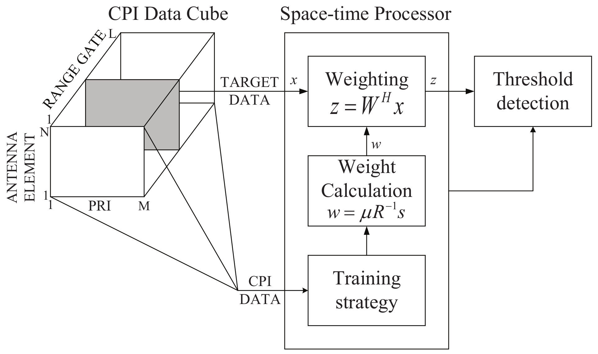
Space-time adaptive processing (STAP) is a signal processing technique commonly used in radar systems [
26,
27]. With the help of the technique, it is possible to achieve order-of-magnitude sensitivity improvements in target detection. According to the addressed array size, the whole calculation amount of STAP is vast (up to 10
to 10
), and the task involves a set of sub-algorithms like matrix covariance, matrix inversion, matrix multiplication, matrix conjugation, division and so on. The goal is to find the optimal space-time weights in NM-dimensional space, where N is the number of antenna elements (our spatial degrees of freedom), and M is the number of pulse-repetition interval (PRI) taps. The detailed algorithm structure diagram is shown in
Figure 7.
In the weight calculating process, the optimal weight vector is expressed as:
where,
is the normalization coefficient. The output of a space-time processor is the weighting result,
. The weighting result then sends out for threshold detection.
The algorithm mentioned above can be decomposed and expressed in MATLAB step by step. The procedure is listed in
Table 1.
Building the application in a compiler environment, the primary work is algorithm API function construction. The API function combination is directly derived from the MATLAB decomposition, and each step listed in the table represents an executable sub-algorithm by RASP. The API calling and data address arrangement should be elaborately organized to fit the task order.
After compiling, a series of bit streams corresponding to each step is generated and stored in the external memory; execution will take place in serial. The source matrix data is stored in external memory, and all the intermediate results are stored and fetched in internal SRAM blocks. The final result data will be sent out for further processing after all the steps are done.
From the implementation point of view, the chosen task is a representative one that involves multiple different operations, revealing the ability of RASP to perform complicated tasks. The amount of calculation is huge and exhibits a certain degree of computation complexity, but the compilation process is convenient and efficient; this property makes it friendly to programmers, and they do not need to learn the detailed information about the hardware implementation process.
5. Prototype Verification Environment
The validation of the proposed accelerator is split into two parts: FPGA prototype verification, and chip testing.
Before tape-out, we build an SoC prototype system based on FPGA not just for algorithm verification but to verify the functional correctness with real peripherals and demonstrate that the software runs end to end, and to create an emulation platform for running long workloads.
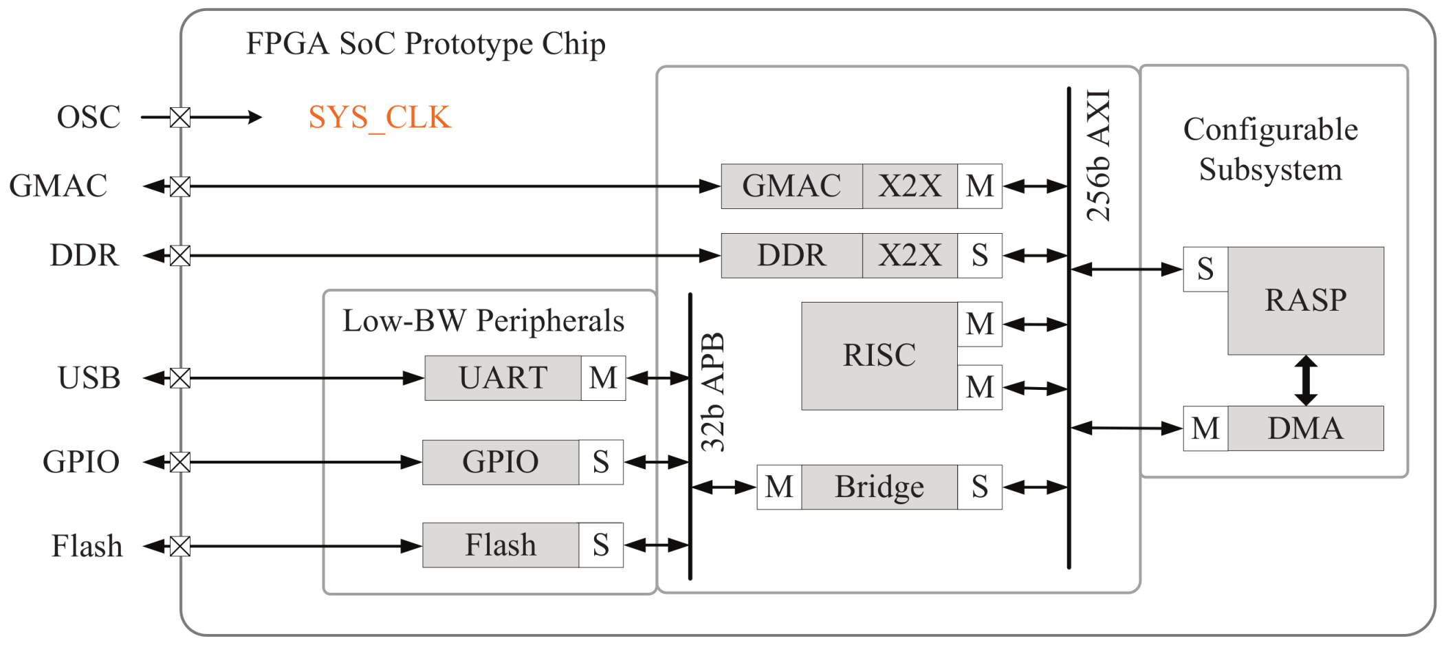
Figure 8 shows the system block diagram of the SoC. It is implemented using Xilinx ISE 14.5 targeting a Xilinx Virtex6-760, and the working frequency is 25 MHz. The RASP engine connects through a 256 bit AXI bus with other components: a Gigabit Media Access Controller (GMAC) for data package switching, a Nor Flash chip to store compiled program bit file, and a universal asynchronous receiver-transmitter (UART) for asynchronous serial communication. The entire SoC consumes 346,192 (73%) LUTs and 560 (78%) RAMB36E1, respectively.
From the system block diagram, we can learn that the proposed accelerator offers good design-reuse opportunities because it is mostly independent of the design of the CPU and the rest of the system. To couple the RASP with different systems, it is sufficient to have a thin hardware wrapper that interfaces its configuration registers and DMA controller with the on-chip interconnect.
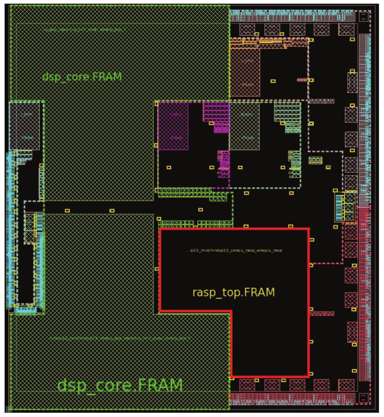
We have also implemented the prototype chip with 40 nm CMOS technology, which has an area of 19.2 mm
and a maximum clock frequency of 1 GHz. The chip layout is shown in
Figure 9; it is integrated with two DSP cores, and the area outlined with a red line is the accelerator subsystem.
Table 2 lists a summary of the RASP chip specifications. Notice that, for the same workload strength, the TI TMS320C6672 consumes 5453 mW with an operating frequency of 1 GHz.
6. Results Analysis
In this section, the performance comparison of a representative algorithm is carried out, the efficiency of complex task execution is discussed, and the precision analysis is also made as a supplement. All the test data of RASP is obtained by running real-life tasks in the prototype chip.
6.1. Performance Analysis
To certify the performance advantage of RASP, the comparison of a representative algorithm–FFT is made. To compare the computation time of FFT, we choose the following processors as the references: a reconfigurable processor MorphoSys [
28], a commercial DSP, and a multicore commercial processors Freescale T4240 [
29,
30], the result is listed in
Table 3 below. In the reference proposals, in order to obtain the clock cycles, Freescale T4240 “assumed that all required instructions and data are present in the L1 cache”, and MorphoSys and TI DSP only count the cycles of computation too. It means that the data used for comparison are about computation phase, so we use the computation time of RASP as the comparison. We can infer from the table that the cycle count of MorphoSys is just a little bigger than RASP; however it should be noted that the computation resource of MorphoSys is two times more than RASP. As for the TI DSP, which has similar computation resources compared with RASP, the RASP can achieve 2.13x speedup. The power consumption is also listed in the table. As a dedicated accelerator, the RASP can achieve speedup with power savings.
The RASP can achieve better performance improvement when dealing with complex tasks. Take STAP as an example, the decomposition of STAP is described in
Table 1 and these steps are executed on different platforms.
Table 4 below lists the detailed cycles of each step of STAP with the dimensions of 32 × 1024.
We are unable to make the statistics about the configuration cycles and data transmission cycles of TI DPS, but the computation cycles of DSP consumes 2.97 times more than the computation cycles of RASP, and 1.74 times more than the total execution cycles of RASP.
Freescale T4240 does better in large-scale vector operations, but when it comes to complex operations such as FFT, matrix multiplication and matrix inversion, it is much worse than RASP due to its software implementation characteristics. Especially for matrix inversion with O(n) algorithm complexity and complex control process, it consumes 2125 times more cycles than RASP. Thus, the total execution cycles are 219 times more than RASP. Taking the working frequency into account (RASP@1 GHz and T4240@1.5 GHz), RASP still gets a 146x speedup.
As described in
Section 4, when RASP executes a complex task, after the procedures of decomposing the task, constructing the API function, and compiling the API, a series of bit stream corresponding to each step is generated and stored in the external memory. Once the task starts, it can be regarded as processes in batch mode. Apart from the first step in the task, the data of the following steps to be processed come from the internal memory, so the data transmission time is eliminated. As mentioned in
Section 3.2, the small chunk of data transmission is very inefficient. From
Table 4 we can see that data transmission between the sub-algorithms occupies 25.36% of the total execution time. It means that compared with the independent execution mode, 25.36% of the whole execution time can be reduced owing to the on-chip scratchpad memory and our approach of complex task execution. Eliminating the data transmission between the tasks of STAP gives it a larger advantage compared with the other platforms.
Therefore, the proposed system can not only yield considerable performance improvement with energy savings but is also capable of complex tasks.
6.2. Precision Analysis
Large-scale matrix operation and multiple iterations may bring about very large numbers, so we choose floating-point for calculations. However, the floating-point numbers can have decidedly worse accuracy than fixed-point numbers in the same word length, so we need to go through an accuracy analysis to ensure precision requirements, especially in the tasks that involve multiple different types of algorithms. For two STAP cases with different dimensions, which are 96 × 4096 and 48 × 2048 respectively, we compare the output data with MATLAB results. The maximum and average square root relative errors are listed below in
Table 5. The data under test are randomly generated single-precision floating-point numbers. According to the results, we observe that the average error is about 5 × 10
and it incurs negligible accuracy loss.
7. Conclusions
This paper introduced an accelerator system with multiple algorithm acceleration modules that is capable of implementing complex radar task with good performance in speed, throughput, and data precision. The aspects addressed by our performance gain analysis include data transmission efficiency, acceleration of algorithm execution, and the convenient in programming. Our results show that external memory accesses are the major efficiency bottleneck for small size algorithm execution, so we use an addressable on-chip memory to improve the throughput of complex tasks. For the given algorithms, the RASP can achieve an average speedup of 1.9× to 10.1× over a state-of-art TI DSP that has similar computing resources. In addition, due to the independence and programming convenience, RASP has the potential as an accelerator attached to a general processor for a broad set of applications.


