Abstract
This study was launched to demonstrate that LEDs at zero bias show recombination photon emissions, and to check the models for the same. A method for measuring the light emission for a LED near zero bias is presented. A large reverse bias sufficient to suppress detectable emissions is assumed. The bias voltage between ‘large reverse’ and our target voltage is modulated, and the difference measured. The measured emissions found are consistent with the Shockley diode equation. The spectrum near zero bias can be measured and characterized. It shows LED behavior that is substantially different from other typical measurements, and suggests a violation of Kirchhoff’s Law.
1. Introduction
This study was launched to demonstrate that LEDs at zero bias show recombination photon emissions, and to check the models for such recombination. LED photon emission near zero bias was explored. A simple apparatus for exploring such condition was developed and demonstrated.
Previously, others [1,2,3,4,5] have explored low voltage LED emissions approaching zero bias using similar apparatus. Santhanam et al. sought to demonstrate refrigeration, so they used a reference of nominal 0 V, effectively measuring on the slope of the signal. We used a reference of nominal −1 V, measuring the signal directly, which allowed for measuring negative voltages and produced a large enough signal for spectral analysis. This paper compares and contrasts the following physical mechanisms that contribute to LED diode photoemission:
- Carrier pairs are generated both thermally and through photogeneration.
- Carrier pairs recombine and emit photons.
- The energy of the emitted photons is a result of Fermi-Dirac statistics for the particular material, and is not inherently the same as Black Body.
- As long as there are carriers present, photo-recombination does not stop, even though carrier density is below intrinsic.
It is therefore our expectation that measurements of diode output spanning zero bias will show non-zero output at zero bias, consistent with calculations of ideal diode current,
where ID is the Diode Current, IS is the Saturation Current, VD is the Diode Voltage, VT is the thermal voltage kBT/q, and n is the ideality factor. The −1 from the ideal diode equation represents equilibrium generation/recombination.
The first approximation for the diode emission is given as,
where symbols are as above.
The above calculations say that generation continues through zero bias (the −1 term), as does recombination (the exponential term). Neither has a discontinuity in the LED output anywhere, including at zero bias.
Non-zero output would be a combination of thermally generated carrier pairs and diffusion of the higher-energy electrons from n-type to active region. The electrons subsequently recombine in the active region and cause photon emissions. We find a carrier recombination temperature which is not consistent with the junction temperature, particularly at higher junction temperatures [6,7,8,9,10,11,12]. This effect is larger than previously noted [10,13]. The spectrum near 0 V suggests a violation of Kirchhoff’s Law.
2. Materials and Methods
The goal of the test method used was to separate photo-emissions of an LED with zero or negative bias (if any) from blackbody emissions. The challenge was that, at near-zero bias, photo-emissions should be small compared to sensitivity of measurement equipment, and near the magnitude of blackbody emissions.
2.1. Approach of Experiment
The general approach was to capture LED spectra, and use a lock-in amplifier to separate blackbody emissions from LED photo emissions. Thermal and recombination emissions from target LED needed to be brought into range of detection by available measurement equipment. Fairly widely-available equipment (a fluorometer and lock-in amplifier) to capture spectra was chosen so that tests could be replicated by others.
Total emissions from target LED were measured under a pair of LED bias conditions—the measured bias and a large reverse bias as indicated in Figure 1—while holding temperature constant. The net emission intensities across a spectrum of a selected LED for forward-biased (lighted) were captured at several voltages and also zero- and reverse-biased.
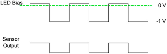
Figure 1.
LED bias voltage and sensor response, showing the modulated voltage signal method where a lock-in amplifier is used to isolate thermally-activated LED photoemission signal only.
A 1650 nm LED, which has a high enough output in the fluorometer range to be useful, was selected. The 1450 nm value from each of the measured bias runs was used because it is the optimal signal for the sensor (brightest signal within its sensitivity range).
The equipment computes the difference in emissions of a pair, thus eliminating contribution by thermal, leaving only the contribution from recombination emission. We computed the exponential function that is the best fit to the intensities at a selected wavelength for the several biases forward biases, including near and below zero.
The automated spectrum sweep was run for 1100 to 1500 nm and selected temperatures and biases.
2.2. Equipment Setup
Figure 2 is an overview diagram of LED Box, Fluorometer, Controller, Signal Generator for bias power, Lock-In Amplifier, Heater Power and control, temperature measurement, data capture hardware, and data capture software of the Fluorolog-3.
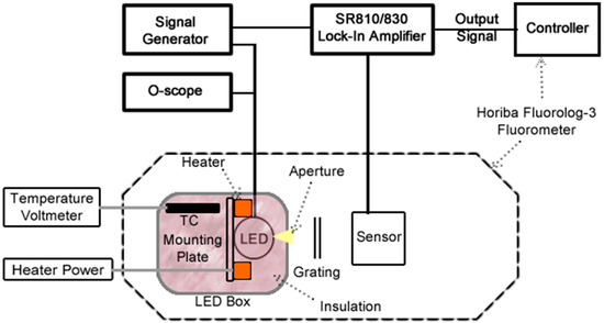
Figure 2.
Test Apparatus schematic, showing major component and connections. LED emits light through LED Box Aperture, which then falls upon the Fluorometer sensor for measurement.
Function/setup of each test apparatus element:
Signal Generator produced a 40 Hz square wave, adjusted for desired output level.
Oscilloscope was used to monitor signal generator output to adjust peak output voltage.
Fluorometer was a Horiba Jobin Yvon Fluorolog-3, with an InGaAs LN 1500 nm sensor and a grating to spread the spectrum across the sensor. Fluorometer control was through Origin software, which allows selecting wavelength and slit width (to control intensity versus selectivity). Wavelength and slit width can be set to specific values (e.g., for 1500 nm runs), or set to step automatically (for whole spectra).
Lock-In Amplifier was a Stanford Research Systems SR810/830. It uses a timing signal and a phase angle to extract the correlated signal (see manual Section 3 SRS810 Basics). A relatively large signal (0.6 V forward, 1500 nm wavelength, 16 nm slit width) was used to calculate the phase angle, and then the setting left fixed for testing. The Lock-In Amplifier scales detected input signals to 10 V output, so if the input range is 500 μV and the signal is 200 μV, output will be 4 V.
Controller was a computer with Origin software by OriginLab.
LED Box (see Figure 3): The outer shell of the LED Box was made of ¼” cement board from Home Depot, dimensioned (to fit within Fluorometer limits) 3 ¼” high, 3 ⅛” wide, 2 ¼” deep and fastened together with screws (see lower left). The aperture is ¼”.
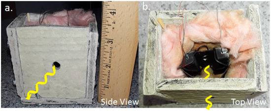
Figure 3.
(a) Front of LED Box, indicating box dimensions and showing aperture. The box is made of cement board and held together with screws. (b) View of Inside of LED Box, showing position of LED (bright spot in center), mounting plate, across top of inside assembly, Heating Power resistors (black cylinders) at left and right. Wires run to Heater Power and Thermocouple Voltmeter.
The Mounting Plate was .032” thick Aluminum. It was held in place by insulation in the LED Box. Insulation was Owens Corning Pink. The Heaters were NTE 10W5D1 10 W 5.1 ohm resistors. The Heaters are connected to the Heater Power by alligator clips. Paperclips retained LED (1) and Heaters (2).
The Thermocouple (TC) was a K-Type, with electrical connection to K-Type connector on Voltmeter. The LED was a Marktech 1650 nm MTE5016-995-IR.
LED Box Contents: (see Figure 3a,b).
Fine copper wires provide bias across the LED. Heavy silvery wires feed power to heating resistors (black topped). Thermocouple and its leads are not in place in this picture. Mounting plate held the heating resistors (wired in series) and the target LED (fastened with a paperclip, the top of which is visible). Target LED is the bright spot on the mounting plate. Black surfaces (tops visible) between heating resistors and front (lower in this view) of LED box were to absorb reflected thermal emissions. They were an extension of the Mounting Plate, wrapped around and painted with high-temperature black.
Heater Power was a 30 V 5 A bench supply
Temperature Voltmeter had a sensitivity of 0.1 °C
Setup Steps—We:
- Placed the LED Box into target enclosure.
- Set the Signal generator to 40 Hz.
- Placed the LED Box in fluorometer.
- Set LED bias to values in the range of 0.60 V to −1.0 V.
- Manually adjusted the LED Box to maximize signal as measured by Lock-In Amplifier. Lock-in phase was set at this time.
2.3. Test Run Controls and Measurements
Temperatures were allowed to come to steady state according to the sensing voltmeter, typically more than five minutes. Intensity measurements for a given temperature and bias were typically taken over minutes to allow time to capture minimum and maximum as the value drifted. These intensity measurement times well-exceeded any transient time for LED behavior and signal generator. The order of run biases was scrambled some, to minimize any effect of temperature measurement drift.
3. Results
This section presents partial raw data from measurements made as described in Section 2, displays test results graphically, and gives some observations about them. Complete raw data are available in Supplementary Materials.
3.1. Measured LED Intensity vs. Bias
Table 1 lists the raw test results at 1450 nm ± 16 nm for a 1650 nm LED at 201 °C, applying the test setup and procedures described in Section 2. Bias voltage is as imposed across the LED. Intensity reading is an arbitrary scale. Since the reading drifted some intensity, especially for low Bias Voltages, the Low and High readings were recorded.

Table 1.
Red Emission Intensity Readings for Bias Voltages.
Figure 4 shows the primary results of our tests. It plots intensity of non-blackbody emission from the target LED versus bias across it, as measured through the fluorometer. Notice that the scale is semi-logarithmic and the points fall near to a straight line.
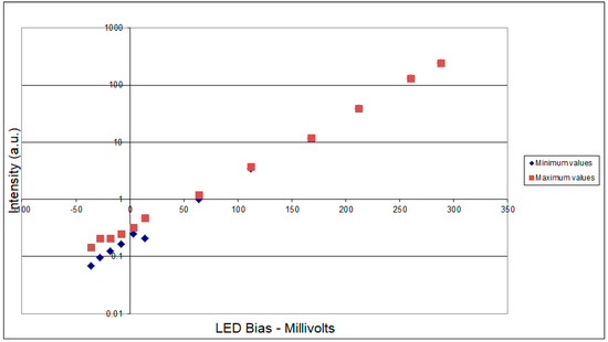
Figure 4.
201 °C LED Intensity vs. Bias Measured at 1450 nm. This semi-log plot shows points falling on a straight line (not shown) that crosses zero bias with non-zero intensity.
We observe that the plots show exponential relationship between bias and intensity of form:
where I0 is the intensity at 0 volts, q is the charge of an electron, V is the diode voltage, n is an ideality factor similar to the Ideal Diode Equation, kB is the Boltzmann constant, and T is the temperature of the diode.
In this case, we calculate that n is 1.03. Also, the intensity is non-zero at zero bias, consistent with intensity vs. bias being an exponential function.
Since the measured high and low values in negative bias still fall near the straight line, we are not yet looking at measurement noise, but actual LED emission. Further, since the plot moving toward the left does not flatten out, blackbody emissions have been properly subtracted out. Otherwise, measured blackbody would begin to dominate the intensity measurement as LED recombination emissions decrease.
3.2. Spectrum Measurements
The following data across the spectrum, made readily available by the fluorometer, was gathered.
Figure 5 and Figure 6 show LED intensity across the spectrum for several temperatures and biases. The key indicates the bias and temperature for each run. To the extent possible, voltages were adjusted to produce an approximately uniform output at 1500 nm. For Figure 6, the horizontal axis is the photon energy as a multiple of kBT for each particular run. All runs were from 1100 nm to 1500 nm. Increasing temperature would move a series to the left because the same wavelength corresponds to a smaller multiple of kBT. Increasing bias would move a series up because it increases the intensity across the entire spectrum.
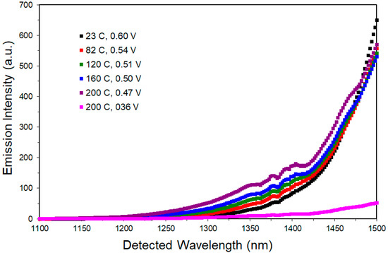
Figure 5.
Intensity vs. Wavelength at Various Temperatures and Bias Voltages. Voltages were chosen to produce the same intensity value at 1500 nm.
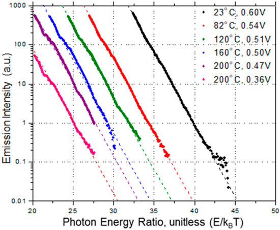
Figure 6.
Intensity versus Photon Energy Ratio at Various Temperatures and Biases. These are the same runs as in Figure 5, plotted with the log of the intensity versus the calculated ratio of photon energy to lattice thermal energy.
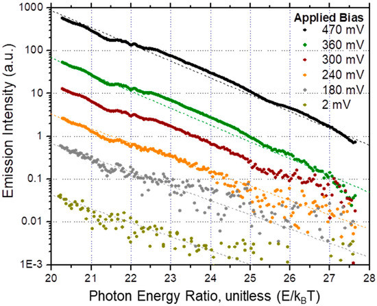
Figure 7.
Intensity versus Photon Energy at 201 °C for Selected Biases.
To the extent possible, voltages were adjusted to produce an approximately uniform output at 1500 nm. For Figure 6, the horizontal axis is the photon energy as a multiple of kBT for each particular run. All runs were from 1100 nm to 1500 nm.
We observe all tests share an exponential curve, notionally based on thermal energy. We find a best fit for this exponent taking form , where n is 1.4 for 201 °C, or an effective temperature of 390 °C. We discuss this further in Section 4.2.
3.3. Possible Sources of Errors in the Measurements
We have given some thought to a few sources of error in the measurement, and taken precautions against them as described below:
Temperature variation between or within runs, including startup for sensor or target:
The LED box was allowed to come to a steady state for at least 5 min before measurements were started. No adjustments were made to the LED Box or heating power for the warm up and duration of the run. Temperature of the LED Box was observed during the runs.
The order of run biases was scrambled some, so that a temperature drift would move data points off the straight line.
Temperature measurement error: Because the thermocouple was not actually in contact with the junction, some error is possible. At 200 °C, varying the location of the thermocouple while keeping it in the vicinity of the LED resulted in changes of 3 °C. Applying a conservative estimate of 9 °C still results in only a 2% error in the measured temperature of 473 K.
Thermoelectric Effect: The leads to the LED had a temperature different across their length of up to 180 °C. For a K-type thermocouple, the thermoelectric effect would give a voltage of 7.4 mV. We mitigated this by using wires cut consecutively from the same spool.
Bias in fluorometer settings: Bias would have to apply exponentially as a function of measured intensity in order to maintain the linear result. Since such bias would not take the plot through zero, the basic conclusion would still stand.
Position of target or sensor between bias runs: The order of runs vs bias was scrambled such that the last five points were taken in the reverse of the order shown in Table 1, which would make such an effect fairly visible in the plot as breaks in the line.
Blackbody feeding LED: Blackbody radiation may be feeding the LED, and may therefore be the source of LED emission near or below zero bias. The Lock-in Amplifier was employed to eliminate that.
Experimenter bias: Since an expected outcome of the experiment was to find a non-zero intensity at zero bias, it may be that the experimenter was simply taking a near-zero reading as non-zero instead of zero. This was addressed by taking readings across a broader range including zero. This allowed us to calculate the slope through zero, interpolate the zero point, and observe whether any of the range of measurements at the bias points were in any way consistent with a zero-zero result.
4. Discussion
4.1. Interpretations, Conclusions, and Expectations
Our work presented here should provide experimental methods that allow exploration around zero bias on LEDs. The measurements away from zero help to confirm the near-zero measurements.
The following interpretations and conclusions were made from Figure 4:
- ○
- The semi-log plot of data shows straight line (within reasonable experimental error) through data points of intensity vs. LED bias voltage.
- ○
- Results are consistent with for shape of Ideal Diode, which adds weight to the validity of the experimental methods.
- ○
- The LED continues to have photo-recombination emissions at and below zero bias.
Our further expectations are that:
- ○
- As bias goes yet more negative, the intensity level would fall below the sensitivity of the fluorometer, so that our measurements would be dominated by noise (scattering from the straight line).
- ○
- As bias goes higher than applied, non-exponential behavior of the LED (Auger recombination and eventually failure) would be seen, so the semi-log plot would no longer be linear.
4.2. Analysis of Properties of Recombination
In Section 3.2, we noted that the high energy tail is not consistent with the measured temperature [6,7,8,9,10,11,12]. For 201 °C, the best fit exponent is roughly 1.4× the measured temperature. We assume that this is due to hot electrons. Under this assumption, the exponent is due to hot electrons injected into the recombination region, and undergoing a partial relaxation. For purpose of discussion, we will call this the ‘recombination temperature’, as defined by the best fit of form . We find it useful to graph the ratio .
4.2.1. Electron Activity around the N-Type Heterojunction
Figure 8 represents electron activity around the n-type heterojunction of a double-heterojunction LED.
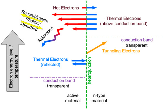
Figure 8.
Relevant Paths for Electrons at the n-type heterojunction of a LED. Note that electrons crossing right to left will initially be at least (delta)Eg above the conduction band (‘Hot Electrons’) and will relax down toward a Fermi-Dirac distribution through collisions.
Under forward bias, some thermal electrons drift/diffuse into the active region and become Hot Electrons. This results in a significant excess of hot electrons. They may undergo some relaxation, including down to thermal levels. Some of these electrons will recombine with a hole, emitting a photon. Some hot electrons will scatter and diffuse back across the junction, again becoming thermal electrons. Some thermal electrons will tunnel and diffuse across the junction. The net result is a recombination temperature which is higher than the junction temperature.
Under reverse bias, drift is in the opposite direction. In this case, the high energy electrons freely drift from the active region into the supporting n-type material. For lower energy electrons, the probability of tunneling is a direct function of the electron energy. The net result is a recombination temperature which is lower than the junction temperature.
4.2.2. Analysis of Measured Results
Figure 9 covers varying temperatures and selected biases. There is a distinct pattern based on temperature. The high quality (V >> 0) runs are all tightly clustered along some curve. Since the heterojunction isn’t changing, we are guessing this reflects different levels of relaxation. It could also reflect an artifact in how we chose the endpoints. All these series used 1300 nm to 1500 nm for extracting the exponent, and the result is sensitive to the energy (not wavelength) of the endpoints. We haven’t probed how it affects the curve.
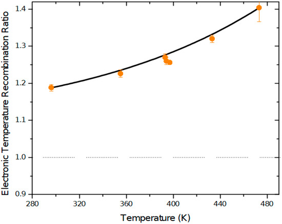
Figure 9.
Temperature Ratio at Various Temperatures, and Voltages V > 5*kBT/q showing the ratio of the computed Spectrum Temperature to measured Junction Temperature. Lower voltages drop below this curve. Figure 10 covers only 200–202 °C at various voltages. At voltages above 240 mV, it seems flat. 176 mV may be part of a trend. The ~0 mV results are all over the place. We would expect that for negative values, the temperature ratio would be less than 1. That is because hot electrons would drift across the heterojunction freely, while lower energy electrons would mostly reflect off it. On this basis, there should be a trend.
This data set is not sufficiently high quality to extract that trend or the value at zero volts. It does, however, suggest a value greater than 1. We expect the exponent term to approach [14]. If photo-recombination were happening in an unbiased LED with an effective temperature other than the lattice temperature, that would point to some kind of challenge to Kirchhoff’s Law and/or the Principle of Detailed Balance. See Figure 10.
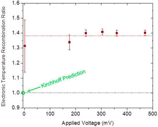
Figure 10.
Temperature Ratios at 201 °C. This shows the ratio of spectrum temperature to junction temperature at 201 °C. Note also that at zero bias, the emission spectrum temperature should be the same temperature as the device.
4.3. Next Steps
This apparatus design was the result of repeated attempts to extract meaningful and interesting data on LED behavior at zero bias. Our first successes were with 1100 nm TE cooled silicon sensors at 200 °C. In comparison, the 1500 nm LN cooled InGaAs sensors offer up rich data at 200 °C. It still falls short of easily extracting the recombination temperature at low and reverse biases. Our experience indicates that the ratio E/kBT plays a large role in determining the quality of the data. The lower the ratio, the more events are available to detect and the higher the signal to noise ratio.
4.4. Summary
This study was launched for the sake of confirming models against actual behavior of LEDs under low bias. Based on use of spectrometer for measurement, it led to evidence of potential Kirchhoff violation. Detailed experimental methods are included to aid in further measurements and studies by others around this conclusion.
Supplementary Materials
The following is available online at http://www.mdpi.com/2079-9292/7/12/360/s1: LED Spectrum Data.xls, which contains the raw data gathered in the experiments described, by Peter Orem, November 2018.
Author Contributions
P.M.O. was the major contributor to this work, from conception to test methods, testing, managing data, analyzing, presenting methods and results, and editing paper. F.M.O. funded this work, organized creation of paper, contributed suggestions on testing methods, and was the principal editor. K.T.V. contributed to system design, test procedures, test execution, data collection, and review. M.W.G. provided the facility, proposed the AC-voltage-modulation lock-in detection scheme, contributed most of the graphs and offered general guidance.
Funding
This research received no external funding. Funding came from Frank and Judy Orem and from Peter Orem. Oregon State University Physics Department has graciously loaned measurement equipment and laboratory time and space to this project.
Conflicts of Interest
The authors declare no conflict of interest.
References
- Santhanam, P.; Fan, S. Thermal-to-electrical energy conversion by diodes under negative illumination. Phys. Rev. B 2016, 93, 161410(R). [Google Scholar] [CrossRef]
- Santhanam, P.; Huang, D.; Gray, D.J.; Ram, R.J. Electro-luminescent cooling: Light emitting diodes above unity efficiency. Laser Refrig. Solids VI Proc. SPIE 2013, 8638, 863807. [Google Scholar]
- Santhanam, P.; Huang, D.; Ram, R.J.; Remennyi, M.A.; Matveev, B.A. Room temperature thermo-electric pumping in mid-infrared light-emitting diodes. Appl. Phys. Lett. 2013, 103, 183513. [Google Scholar] [CrossRef]
- Gray, D.J.; Santhanam, P.; Ram, R.J. Design for enhanced thermo-electric pumping in light emitting diodes. Appl. Phys. Lett. 2013, 103, 123503. [Google Scholar] [CrossRef]
- Santhanam, P.; Gray, D.J.; Ram, R.J. Thermoelectrically Pumped Light-Emitting Diodes Operating above Unity Efficiency. Phys. Rev. Lett. 2012, 108, 097403. [Google Scholar] [CrossRef] [PubMed]
- Baumgartner, H.; Vaskuri, A.; Kärhä, P.; Ikonen, E. Temperature invariant energy value in LED spectra. Appl. Phys. Lett. 2016, 109, 231103. [Google Scholar] [CrossRef]
- Lock, D.A.; Hall, S.R.G.; Prins, A.G.; Crutchley, B.G.; Kynaston, S.; Sweeney, S.J. LED Junction Temperature Measurement Using Generated Photocurrent. J. Display Technol. 2013, 9, 396–401. [Google Scholar] [CrossRef]
- Raypah, M.E.; Devarajan, M.; Sulaiman, F. Modeling Spectra of Low-Power SMD LEDs as a Function of Ambient Temperature. IEEE Trans. Electron Devices 2017, 64, 1180–1186. [Google Scholar] [CrossRef]
- Vaitonis, Z.; Vitta, P.; Žukauskas, A. Measurement of the junction temperature in high-power light-emitting diodes from the high-energy wing of the electroluminescence band. J. Appl. Phys. 2008, 103, 093110. [Google Scholar] [CrossRef]
- Vaskuri, A.; Baumgartner, H.; Kärhä, P.; Andor, G.; Ikonen, E. Modeling the spectral shape of InGaAlP-based red light-emitting diodes. J. Appl. Phys. 2015, 118, 203103. [Google Scholar] [CrossRef]
- Keppens, A.; Ryckaert, W.R.; Deconinck, G.; Hanselaer, P. Modeling high power light-emitting diode spectra and their variation with junction temperature. J. Appl. Phys. 2010, 108, 043104. [Google Scholar] [CrossRef]
- Lin, Y.; Gao, Y.L.; Lu, Y.J.; Zhu, L.H.; Zhang, Y.; Chen, Z. Study of temperature sensitive optical parameters and junction temperature determination of light-emitting diodes. Appl. Phys. Lett. 2012, 100, 202108. [Google Scholar] [CrossRef]
- Chen, N.; Lien, W.C.; Yang, Y.K.; Shen, C.; Wang, Y.S.; Chen, J.F. Spectral shape and broadening of emission from AlGaInP light-emitting diodes. J. Appl. Phys. 2009, 106, 074514. [Google Scholar] [CrossRef]
- Brody, J.; Weiss, D.; Young, P. Observing the Maxwell-Boltzmann distribution in LED emission spectra. Am. J. Phys. 2010, 78, 933–935. [Google Scholar] [CrossRef]
© 2018 by the authors. Licensee MDPI, Basel, Switzerland. This article is an open access article distributed under the terms and conditions of the Creative Commons Attribution (CC BY) license (http://creativecommons.org/licenses/by/4.0/).