Article

Equivalent Circuit Model for Cu(In,Ga)Se2 Solar Cells Operating at Different Temperatures and Irradiance

by
Matteo Bronzoni
1,†,
Lorenzo Colace
2,†,
Andrea De Iacovo
2,†,
Antonino Laudani
2,*,†,
Gabriele Maria Lozito
2,†,
Valentina Lucaferri
2,†,
Martina Radicioni
2,† and
Stefano Rampino
1,†
1
Institute of Materials for Electronics and Magnetism, National Research Council (IMEM-CNR), Parco Area Delle Scienze 37/A, 43124 Parma, Italy
2
Department of Engineering, University Roma Tre, Via Vito Volterra, 64, 00146 Rome, Italy
*
Author to whom correspondence should be addressed.
These authors contributed equally to this work.
Electronics 2018, 7(11), 324; https://doi.org/10.3390/electronics7110324
Submission received: 18 October 2018 / Revised: 8 November 2018 / Accepted: 12 November 2018 / Published: 15 November 2018
(This article belongs to the Section Microelectronics)

Abstract

:
The modeling of photovoltaic cells is an essential step in the analysis of the performances and characterization of PV systems. This paper proposes an experimental study of the dependence of the five parameters of the one-diode model on atmospheric conditions, i.e., irradiance and temperature in the case of thin-film solar cells. The extraction of the five parameters was performed starting from two sets of experimental data obtained from Cu(In,Ga)Se2 solar cells fabricated by the low-temperature pulsed electron deposition technique. A reduced form approach of the one-diode model has been adopted, leading to an accurate identification of the cell. It was possible to elaborate suitable relations describing the behavior of the parameters as functions of the environmental conditions. This allowed accurately predicting the trends of the parameters from a pair of curves, instead of a whole set of measurements. The developed model describing the dependence on irradiance and temperature was validated by means of a large set of experimental measurements on several Cu(In,Ga)Se2 (CIGS) devices built with the same technological process.

1. Introduction

Thin-film solar cells are commonly considered the second generation of photovoltaics, and their market penetration is rapidly expanding, thanks to their competitive costs with respect to traditional silicon cells. Mainly, this is due to the higher absorption coefficient of polycrystalline chalcogenides, so that a few micrometers of material are enough to absorb most of the sunlight, contrary to Si, which requires 100–200 µm. In particular, Cu(In,Ga)Se2 (CIGS) [1] is the quickest expanding thin-film technology, despite the expensive fabrication costs required for standard multiple-stage cell production routes based on sputtering [2], thermal co-evaporation [3] and the notable NRELthree-stage CIGS deposition process [4]. Nowadays, lab-scale CIGS solar cells with a conversion efficiency ≈23% have been obtained [5]. Low-Temperature Pulsed Electron Deposition (LTPED) is a novel and less expensive alternative growth technology for depositing CIGS on a variety of different substrates including ultra-lightweight metal foils and thermolabile substrates, with no need for post-deposition treatments like selenization or high temperature annealing [6]. Thanks to the combination of low substrate temperatures (≈250 °C) and the unique properties of the single-stage PED ablation process, solar cells with efficiencies up to 17% have been fabricated [7]. The huge expansion experienced by CIGS-based PV technology in this last decade needs suitable tools to estimate and predict the power generation of CIGS-based PV systems. Recent studies on the current-voltage characteristics of CIGS addressed some issues on modeling, such as in [8] or in [9], where analytical models of the J-V characteristics of CIGS-based thin film solar cell was proposed, starting from the study of the junction parameters. On the other hand, few works, to the authors’ knowledge, have taken into account the dependence of the current-voltage characteristic on irradiance and temperature conditions. In particular, in [10], an analysis of the current-voltage curves of a CIGS solar cell from experimental data for different irradiation conditions was proposed. In the cited work, an analysis featuring high irradiance levels (from 1–5 Sun at steps of 0.5 Sun) was taken into account. A specific modified double diode model was proposed, and the dependence of the model parameters on irradiance level was investigated. Unfortunately, the temperature influence on the parameters is omitted both in terms of modeling and in terms of experimental study. The most complete analysis proposed in the literature is probably the one in [11], where an analytical model for CIGS, with dependence on illumination and temperature, is presented. In this paper, starting from a physical model of the junction, a modified version of the one-diode model is presented, where the circuital parameters depend nonlinearly on voltage, irradiance and temperature. This model seems to be extremely complete and, in theory, could be used to predict the power production for a PV system based on CIGS. In terms of usage, it requires a fitting procedure based on current-voltage curves from both dark and illuminated (for example at 1 Sun) conditions, and consequently, it is easily implementable. The main inconvenience is related to the analytical model. The model was developed on CIGS cells featuring moderately high efficiency (as stated by the authors) and requires further analysis for general CIGS cells. These results seem to suggest the necessity for a modified and specific model for CIGS, since the direct adoption of the available model for Si-based devices cannot ensure the required accuracy. Moreover, the study of tailored models for the different technologies is still an open issue [12,13,14,15,16]. Indeed, each PV technology has different characteristics, and only experimental characterization, together with suitable models, allows gaining insight into its behavior. In general, the most widely-used circuital representation for the description of the current voltage relationship of PV cells is the one-diode (or five-parameter) model [17,18], whose lumped circuital parameters can be identified either from datasheet information [19,20] or from experimental data [21]. Clearly, the current-voltage curve depends on environmental conditions, and consequently, even for such a model, the lumped parameters of the circuital model change according to solar radiation and cell temperature [18]. For this reason, it is important to study this dependency for each parameter and develop, for each different technology, a complete model able to take into account this effect and predict the current-voltage curve in any environmental condition. The bottleneck of this kind of approach is the effectiveness of the model extracted, since it is affected by the error in the identification of the circuital parameters: indeed, to identify the model, it is necessary to solve a least squares problem involving noisy experimental data, which is a non-trivial task. The main critical issues of this problem are the size of the solution space and the choice of the initial values of the parameters. These issues have also led to some erroneous considerations about the validity of the one-diode model for different technologies, due to the extraction of non-physical meaning parameters. In some cases, other circuital models employing a higher number of diodes have been adopted [12,14], but this leads to further difficulties in the solution of the identification problem due to a higher number of parameters involved. However, as already shown in [21], the dimension of the search space for the one-diode model can be decreased by using the so-called reduced forms: this approach reduces the number of unknowns of the problem from five to two, making it possible to solve the least squares problem with efficient and simple deterministic methods. Following this approach, significant benefits can be achieved, such as a reduced execution time and better convergence, while preserving accuracy. In addition, the extracted parameters have physical meaning thanks to the tailored boundary, and for this reason, they can be successfully used to model the cell behavior. For example, by observing the trends of the extracted parameters with changing environmental conditions or after prolonged exposure, it is possible to elaborate precise relations for the aforementioned parameters [22].
In this work, we performed the experimental characterization for CIGS solar cells grown by LTPED and the successive set up and validation of a mathematical model based on a one-diode circuit, describing the dependence on irradiance and temperature for each circuital parameter. Our approach is based on two steps. In the first one, the identification of the five parameters of the one-diode model was performed for each available experimental current-voltage curve, i.e., for different values of irradiance and temperature. In the second, a mathematical model expressing the parameters’ dependence on the environmental conditions was built from these preliminary results by exploiting a trial and error approach. The proposed model was then validated by evaluating its error on current-voltage curves different from those used for the extraction of the parameters. The results show the possibilities of the adoption of the proposed model for the prediction of current voltage behavior for different environmental conditions.
Since CIGS devices are becoming increasingly common in commercial application, an accurate circuit model can benefit technological transfer for consumer-specific applications such as maximum power point tracking, estimation of the energy production and aging assessment of the modules.
The paper is structured as follows: in Section 2, the experimental setup and the obtained measurements are described; in Section 3, the problem of the identification of the one-diode model from the available data is addressed; in Section 4, the model proposed for the dependence of the circuital parameters on irradiance and temperature is presented and then validated against an independent device set in Section 5. Conclusions and final remarks follow in Section 6.

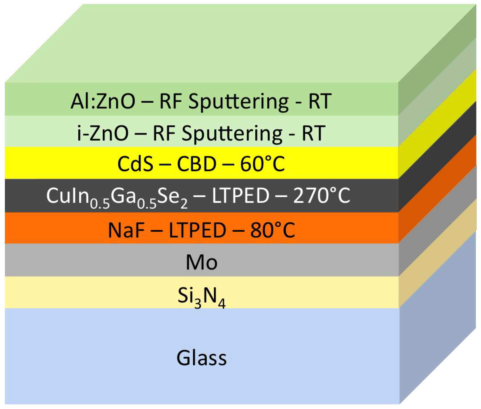
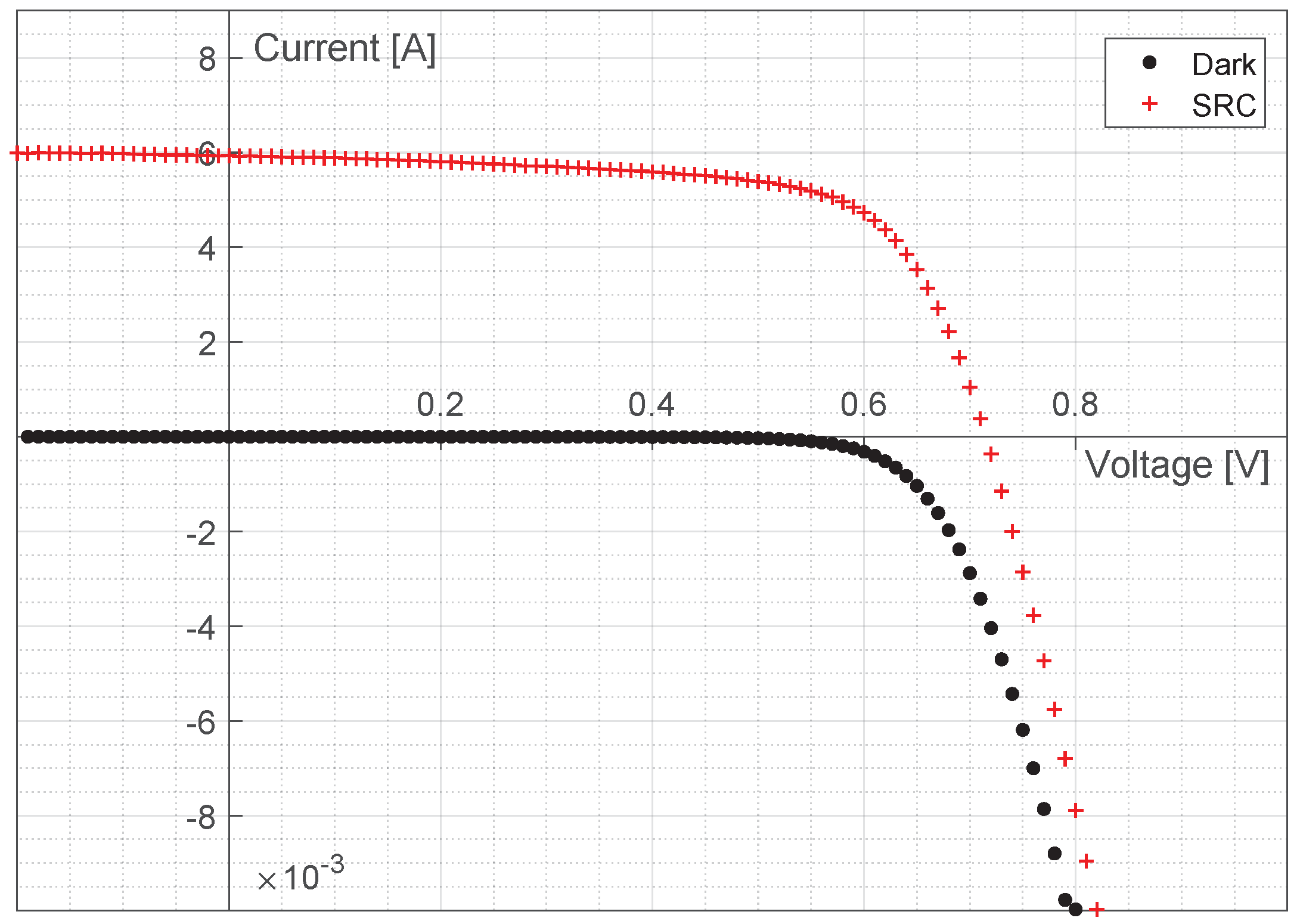
2. Experimental Setup and Measurements

A preliminary part of the project dealt with measuring the experimental current-voltage (I-V) characteristics of CIGS solar cells to be used in the subsequent modeling phase. Thin-film CIGS cells were grown on soda-lime glass substrates coated with a Si3N4 blocking layer and a 0.5 µm-thick Mo contact. A sodium-reservoir NaF layer was deposited by LTPED at a substrate temperature of 80 °C to a thickness of the order of 8–10 nm. After the temperature of the deposition surface was increased up to 250 °C, the CIGS absorber with a Ga/(In + Ga) ratio = 0.5 was grown by LTPED up to a thickness of about 1.6 µm, monitored in situ by an IR pyrometer. The solar cells were then completed with a 70 nm-thick CdS n-type buffer layer grown by Chemical Bath Deposition (CBD), followed by 50 nm of undoped ZnO and 250 nm of Al:ZnO, both deposited by RF-sputtering. Al contacts (1 µm thick) were finally thermally evaporated on the top surface. The details about the structural and the morphological properties of LTPED CIGS solar cells can be found in previous works [6,7,23]. The representative scheme of the solar cell architecture is shown in Figure 1. From a single fabrication batch, a set of 16 different cells with a total area of 0.25 cm2 was defined by mechanical scribing. Every cell was characterized under Standard Reference Conditions (SRC) (25 °C, AM1.5spectrum and 100 mW/cm2) using the following experimental setup:
  • A class ABB solar simulator equipped with a xenon lamp was used to reproduce the solar spectrum;
  • three air mass filters were used to shape the spectrum;
  • a system to sense and tune the temperature of the cells made by a thermocouple, a Peltier cell and a temperature controller was used to set and check cell temperature;
  • a curve-tracer was used to extract the current from the cells by setting a voltage in the range [−0.2, 1] V with a step of 0.01 V;
  • a calibrated test cell measured the irradiance;
  • all the acquisition and measurements were controlled by a LabVIEW interface.
The average electrical parameters of the cells and the relating standard deviations are summarized in Table 1.
One of these cells was measured to obtain two sets of curves, varying the two main environmental parameters: irradiance and temperature. The first dataset was collected by maintaining the level of irradiance at 100 mW/cm2 and increasing the temperature from 25–55 °C with a step of 5 °C. The second set was obtained by setting the temperature at 25 °C and varying the irradiance S in the range [30, 130] mW/m2 with a step of 20 mW/cm2. The dataset of each curve is made up of 120 samples; the measured curves are shown in Figure 2 and Figure 3.
For the sake of completeness, in Figure 4, a dark (0 mW/cm2 and 25 °C) vs. SRC (100 mW/cm2 and 25 °C) measurement is reported. This measurement allows assessing the difference between voltage-dependent collection and the shunt effect and is important for a physical interpretation of the device operating behavior. Indeed, for a complete physical investigation of the device behavior, larger ranges in temperatures and irradiances should be considered, especially for better understanding of the transport phenomena inside the solar cells. For further details, valid results can be found in [24,25].
Lastly, the trends observed for the cells’ open-circuit voltage and short-circuit current versus irradiance and temperature are reported, respectively, in Figure 5 and Figure 6. Characterization has been performed on multiple cells, and the trends do not differ significantly from the ones reported in the figures.

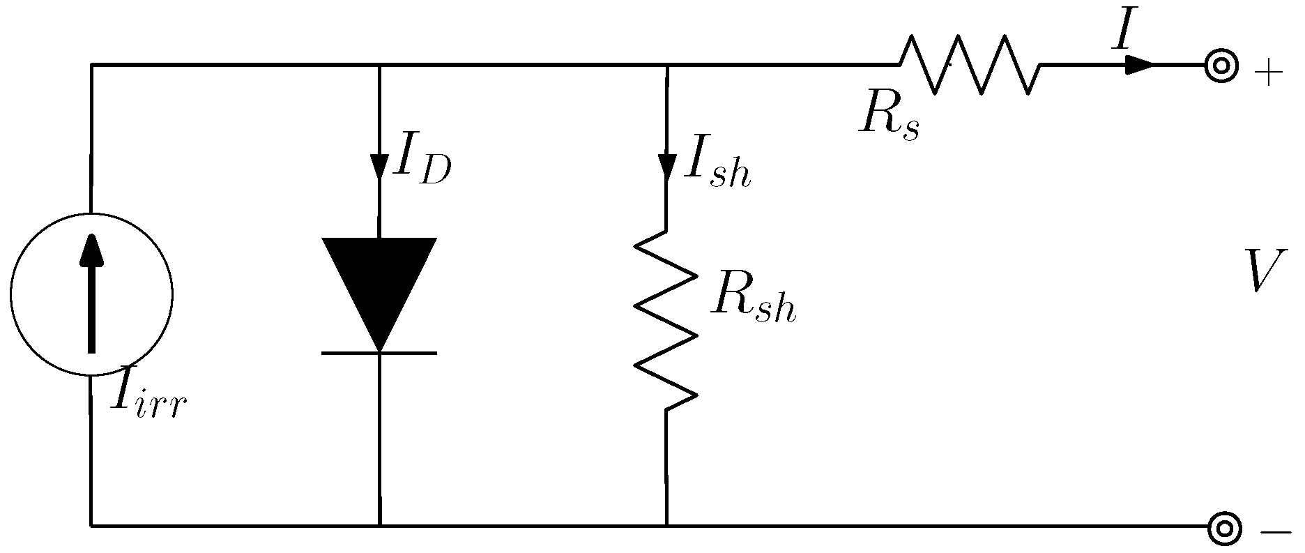
3. Identification of the One-Diode Model from Measurements

The one-diode model is the lumped parameter circuit shown in Figure 7, consisting of an ideal current source I i r r , addressed as photo-generated current (depending on solar radiation level), a diode connected in parallel with a current I D , a shunt current I s h triggered by the shunt resistance R s h and a series resistance R s . The equation characterizing the current I and voltage V is:
I = I i r r I D I s h = I i r r I o e ( V + I R s ) / ( n V T ) 1 ( V + I R s ) / R s h
where n and I o are the ideality factor and the reverse current of the diode, respectively, while V T is the thermal voltage. In Equation (1), V and I stand for cell output voltage and current, respectively. Although this circuital model might seem simple, it is able to describe accurately the current-voltage behavior of different PV cell technologies [19] and can be used for several interesting PV-related applications, such as irradiance measurement [26,27], device degradation assessment [28] and maximum power point tracking [29,30,31,32,33]. As stated before, the main problem in the use of this circuital model is the extraction of its parameters from measured current-voltage curves. Indeed, this requires the solution of a Least Squares Problem (LSP) with the five unknowns θ 5 = I i r r , I o , n , R s h , R s in an extremely large search space, that is the minimization of the Squared Error (SE):
S E = n = 1 N I n f I ( V n , θ 5 ) 2
where N is the number of samples, V n and I n are the vectors of voltage and current measured samples and f I ( V n , θ 5 ) is the computed current by solving Equation (1) for assigned V n . In order to avoid unrealistic solutions related to local minima of Equation (2), deterministic methods (based on the Newton–Raphson approach) should be avoided. Consequently, stochastic approaches with elevated computational costs are often used [19,21]. Nevertheless, this does not guarantee the optimality of the found solution, and it is still necessary to repeat the minimization process several times. A few years ago, an effective approach had been proposed to solve this problem quickly [19,20,21]. This approach is based on the reduction of the unknowns of the problem by means of the so-called “reduced forms” of the one-diode model. In fact, in [19], it has been demonstrated, through algebraic manipulations, that the ideality factor n and the series resistance R s can be used as unique independent variables, by exploiting voltage and current data in Open-Circuit (OC), Short-Circuit (SC) and Maximum Power Point (MPP) conditions. This allows solving the same problem with:
θ 5 = [ I i r r ( n , R s ) , I 0 ( n , R s ) , n , R s h ( n , R s ) , R s ]
where the relations I i r r ( n , R s ) , I o ( n , R s ) and R s h ( n , R s ) are the ones presented in [19]. Thus, we define the effective unknowns’ vector as:
θ 2 = [ n , R s ]
This choice leads to the possibility of reducing the size of the search space and implementing, in the MATLAB environment, a deterministic optimization algorithm based on the least squares method, removing the necessity of using complex and computationally-demanding algorithms. In this case, a deterministic approach operates well enough, since the two unknowns are bounded and a minimum can be easily found for the problem [21]. Clearly, the solution found is affected by error due to the hypothesis that OC, SC and MPP were exact. Indeed, those values are extrapolated from available measurement, and consequently, this can greatly influence the solution found by using reduced forms. Still, as explained in [21], the found solution can be used as an initial guess for the complete minimization problem (with five unknowns) of Equation (2) by means of a deterministic method, since, in this case, we are sure that a good initial guess has been chosen. Additional details on this approach can be found in [19,21]. Thus, the procedure adopted can be outlined in the following steps:
  • Initial determination of the model parameters by solving the reduced-form problem (i.e., extraction of n and R s ). The problem is solved by means of the least squares method on I-V curves in the voltage range (0– V o c ). The algorithm iteratively adjusts [n, R s ] by minimizing the squared error between computed and measured current samples.
  • Re-solution of the problem in complete form with the I-V curves in the voltage range [−0.2, 1] V starting from the solution found in the previous part. The results of this latest step are reported in Table 2 and Table 3 for different values of irradiance and temperature.

4. Model for Irradiance and Temperature Dependence

The extracted parameters have been used to gain insight into their dependence on irradiance and temperature. This was done in order to develop a model able to predict the current-voltage relationship for different environmental conditions, i.e., for different temperature and irradiance values. In particular, we consider the dependence on temperature and irradiance separately, aiming at developing simple expressions. The first model investigates the temperature dependence, and the second investigates the irradiance dependence.

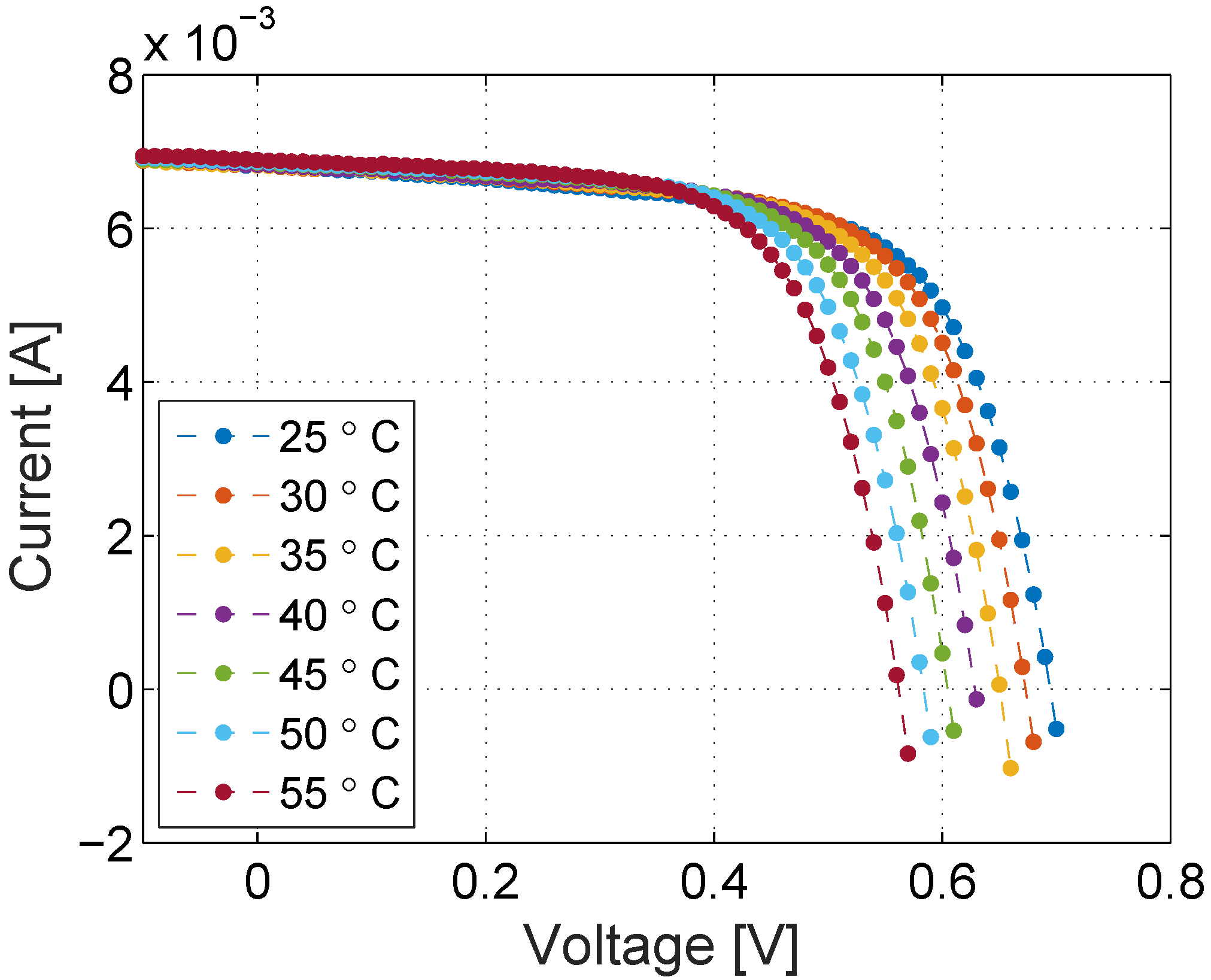
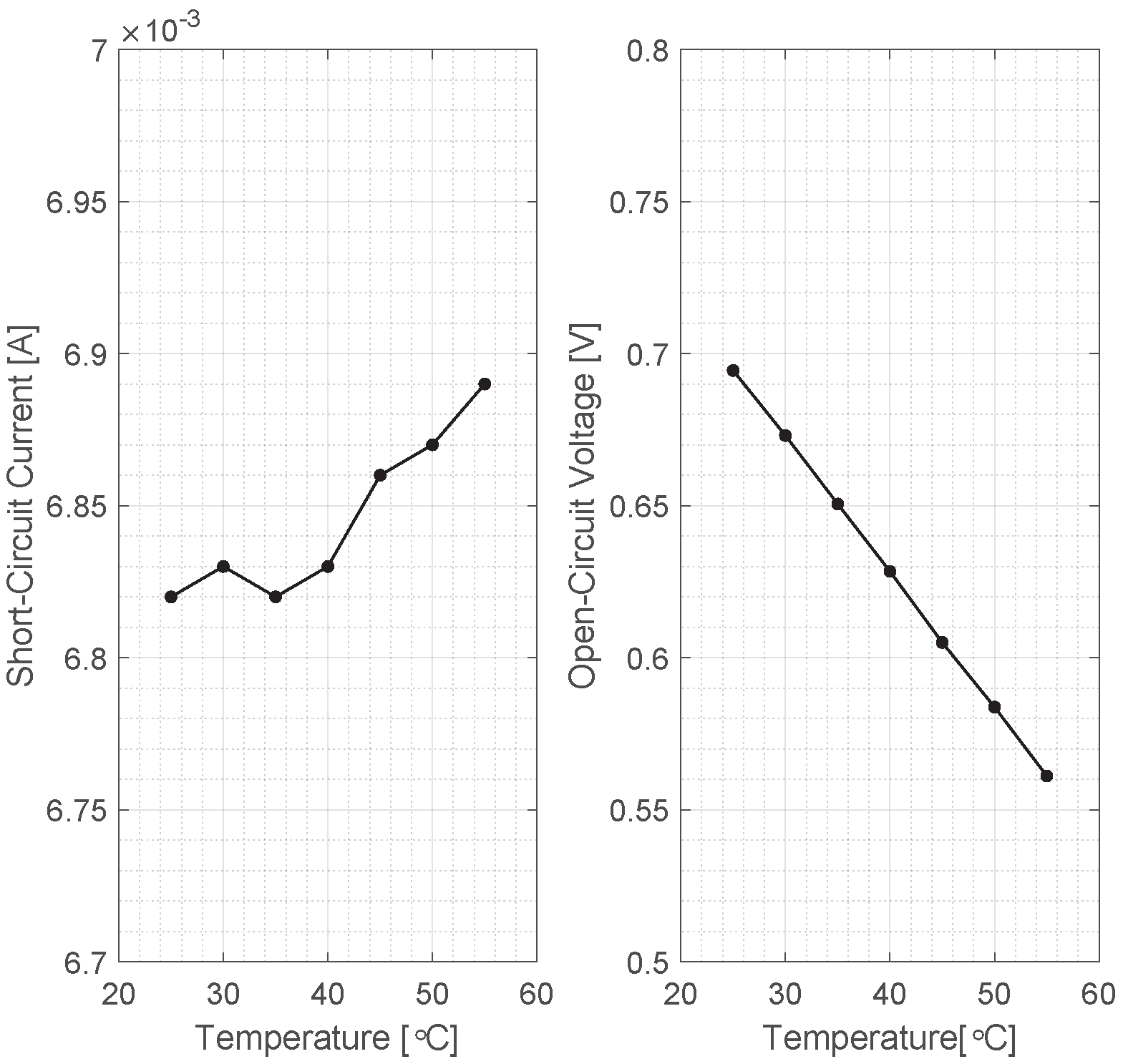
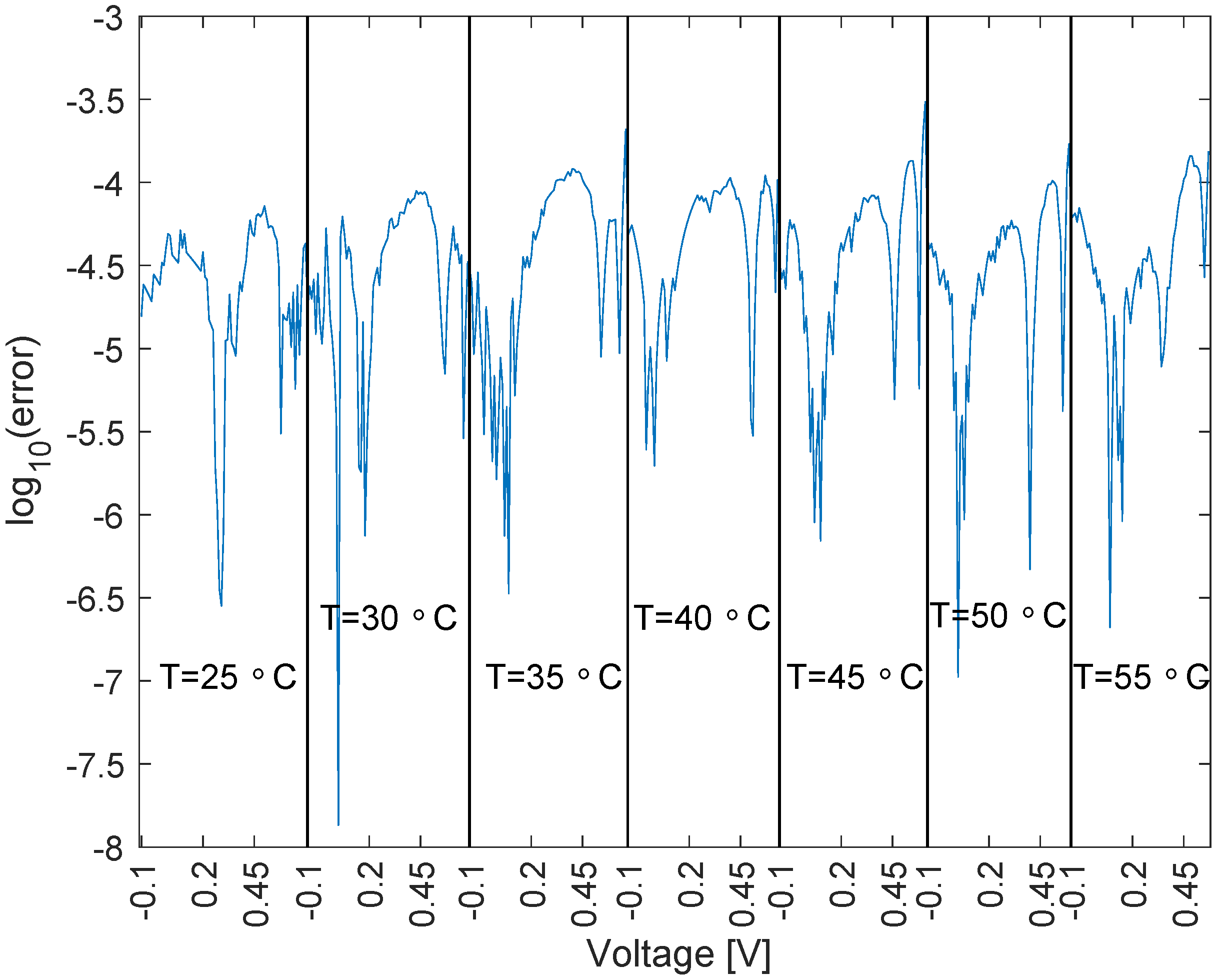
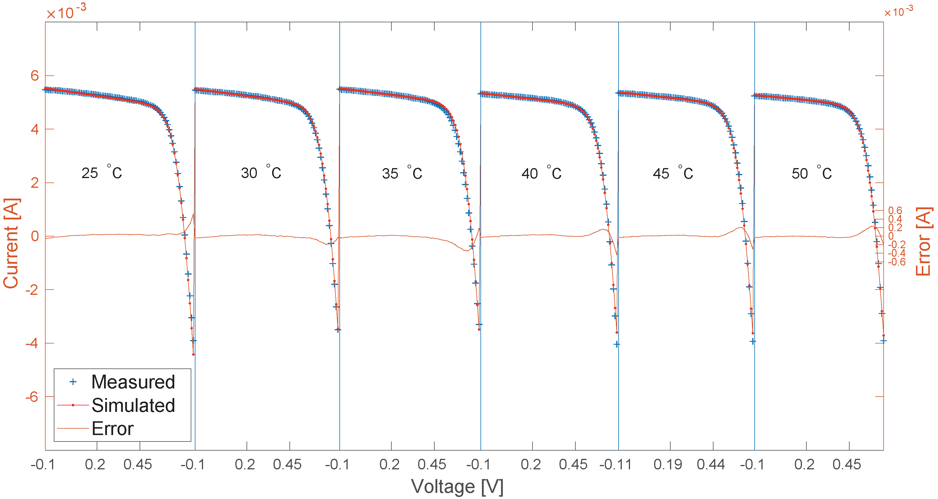
4.1. Temperature Set
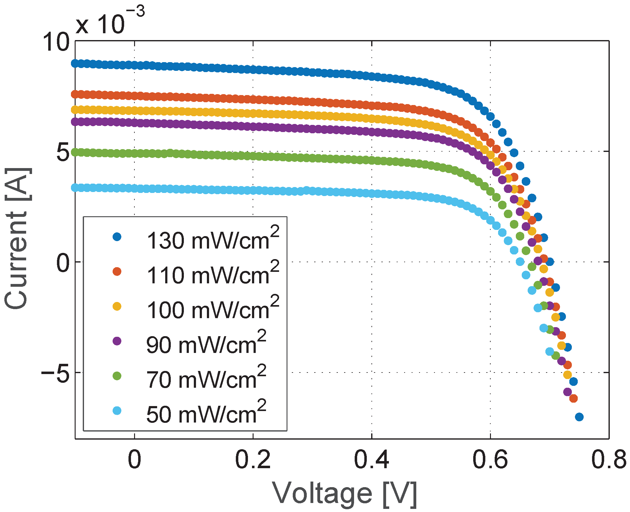
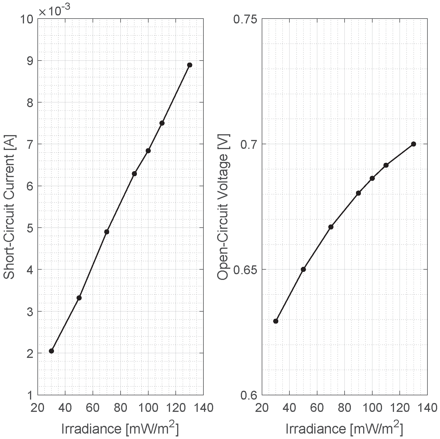
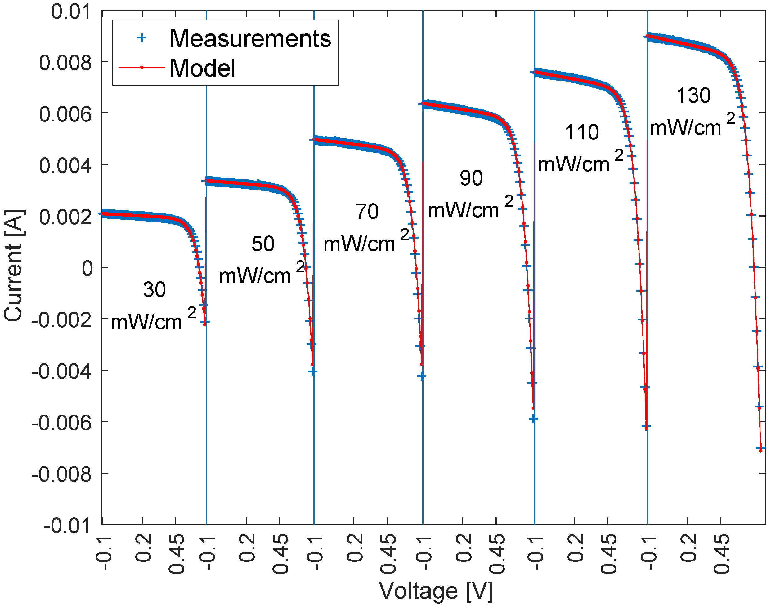
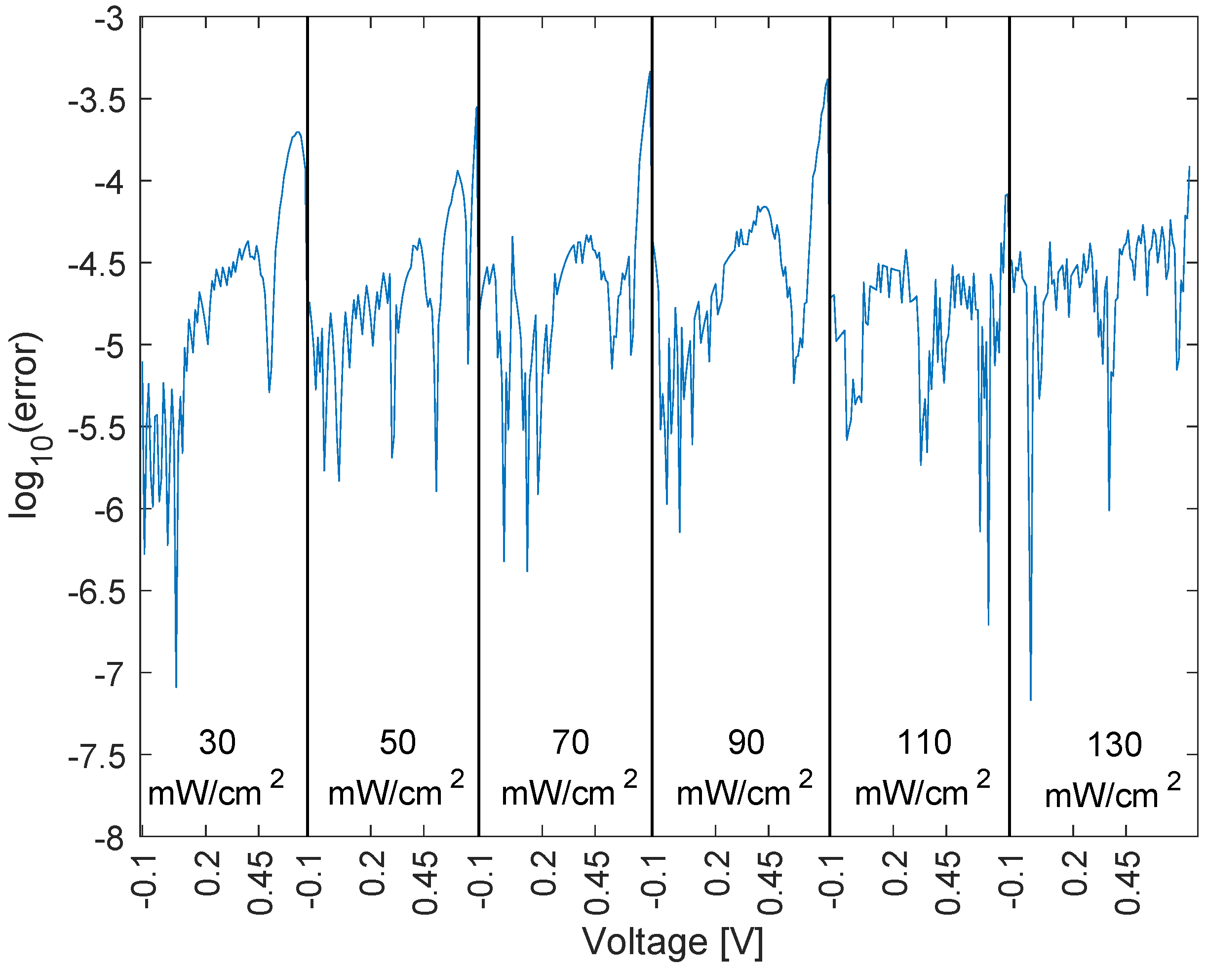
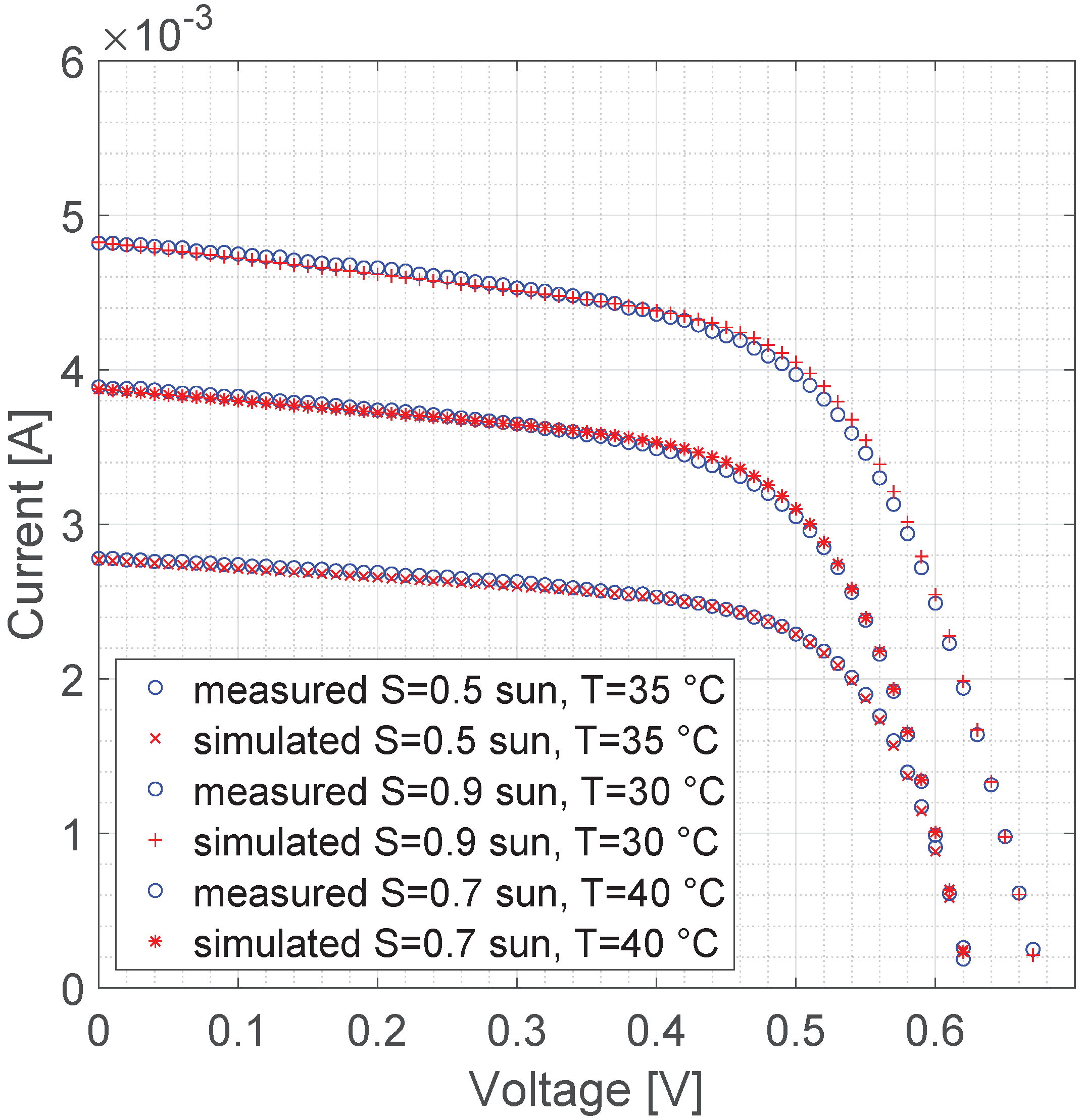
Concerning the n and R s parameters, no clear trend with temperature was observed. Therefore, they have been assumed as constant. On the other hand, concerning I 0 , I i r r and R s h , we started with a simple expression related to the typical dependence of these parameters. In the following, we use the subscripts ref to identify parameters at Standard Reference Conditions (SRC) [18]. For I i r r , we consider a linear dependence, as expected by the traditional one-diode model, and later confirmed by parameters validation:
I i r r = I i r r , r e f ( 1 + α Δ T ) = I i r r , r e f + α Δ T
For R s h , a similar dependence has been assumed. After some trial and error with different formulae, we concluded that the following linear dependency guarantees a good accuracy:
R s h = R s h , r e f ( 1 + γ Δ T )
The expression for I o is similar to the one usually employed for a standard Si-based PV cell:
I o = I o , r e f T T r e f 3 e E g , r e f k B T r e f E g ( T ) k B T
where k B is the Boltzmann constant. Yet, in this case, we should consider two main problems: the first is the difficulty to establish the value of E g , r e f , that is the band gap energy at SRC; the second is the further dependence of E g ( T ) on temperature T. In order to overcome both problems, we proposed a linear dependence for E g ( T ) ,
E g = E g , r e f + c · Δ T = E g , r e f + c · ( T T r e f )
Then, by manipulation of the argument of the exponential, we found:
I o = I o , r e f T T r e f 3 e β ( T T r e f ) T · T r e f
where the only remaining unknown coefficient β is equal to ( E g , r e f c · T r e f ) / k B . It is worth noticing that the previously-presented relation was found by a trial and error approach, starting from a hypothetical relationship that was later refined by validating it against current-voltage curves at different temperatures. To do this, we have considered the available samples related to temperature set measurements. Each sample is composed of the triplet ( I k , V k , T k ). The unknowns of the fitting problem are the five parameters of the one-diode model and the coefficients α , β and γ :
θ 8 = I i r r , I 0 , n , R s h , R s , α , β , γ
The objective function to be minimized is:
S E = k = 1 N s a m p l e [ I k f I ( V k , T k , θ 8 ) ] 2
In this case, as well, we used a two-stage approach. In the first stage, we used the whole dataset available to verify the capabilities of the formulas and parameters added to describe the temperature relation. In the second stage, we used only two or three current-voltage curves for the fitting of the parameter and then used the found parameters to verify the performance in the prediction of all available samples. As stated before, the set of formulas introduced was effective, and the mean squared error found during the fitting by using all the available data was 2.768 × 10⁻⁹. Figure 8 shows the comparison between the measured current-voltage characteristics taken from Figure 2 and the simulated values for all available samples. Figure 9 plots the error between measured and simulated samples. It is easy to note that the error is almost always below 1 × 10⁻⁴ A.
The results related to the second stage are reported in Table 4, where the Mean Absolute Error (MAE) found in the evaluation of all the available data for the three different datasets used for the fitting is presented. In particular, Case 1 refers to the two current voltage curves at 30 °C and 45 °C; Case 2 refers to the two current voltage curves at 35 °C and 55 °C; and Case 3 refers to the three current voltage curves at 20 °C, 40 °C and 55 °C. It is worth emphasizing that the Mean Squared Error (MSE) does not differ significantly from the one achieved by using all the available data in the fitting.
Since the order of the magnitude of the error does not vary significantly, it has been concluded that a single couple of measurements is sufficient to identify the cell and hence to provide the five parameters of the one-diode model; this avoids the acquisition of a whole set of measurements and prevents errors that generally affect this stage. In support of the fact that the choice of the particular set of curves does not affect the result, the values of the five parameters of the model are shown in Table 5 for the aforementioned cases of study.

4.2. Irradiance Set

For the dependence on irradiance, we performed an analysis analogous to the previous one for temperature. By observing the measured parameters, it is evident that I o ,n and R s do not change significantly with irradiance, whereas for I i r r and R s h , the following trends have been assumed, respectively (where S is the irradiance measured in mW/cm2):
R s h = R s h , r e f 100 / S
I i r r = I i r r , r e f S / 100
We repeated the same procedure as for the previous case. For the sake of simplicity, only the results obtained by using a couple of curves, and the ones later refined on the whole dataset, are reported.
As in the previous case, the use of the whole dataset reduces the value of the error. Still, the results obtained with a pair of curves are quite accurate. The comparison between the measured current-voltage characteristics in Figure 3 and the simulated curves is shown in Figure 10. The corresponding mean absolute error is reported in Figure 11.
It can be noticed that, as in the case of varying the irradiance, the value of MAE is maintained around 10−4; thus, even in this case, the method is able to identify the cell accurately.

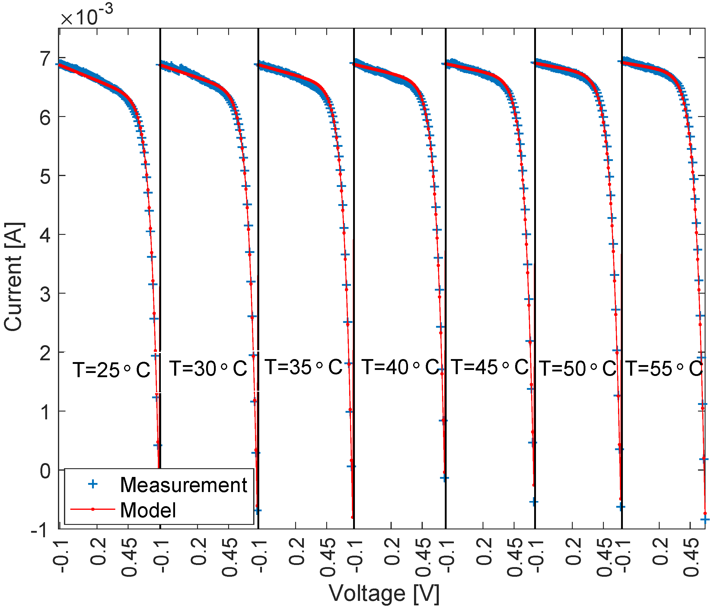
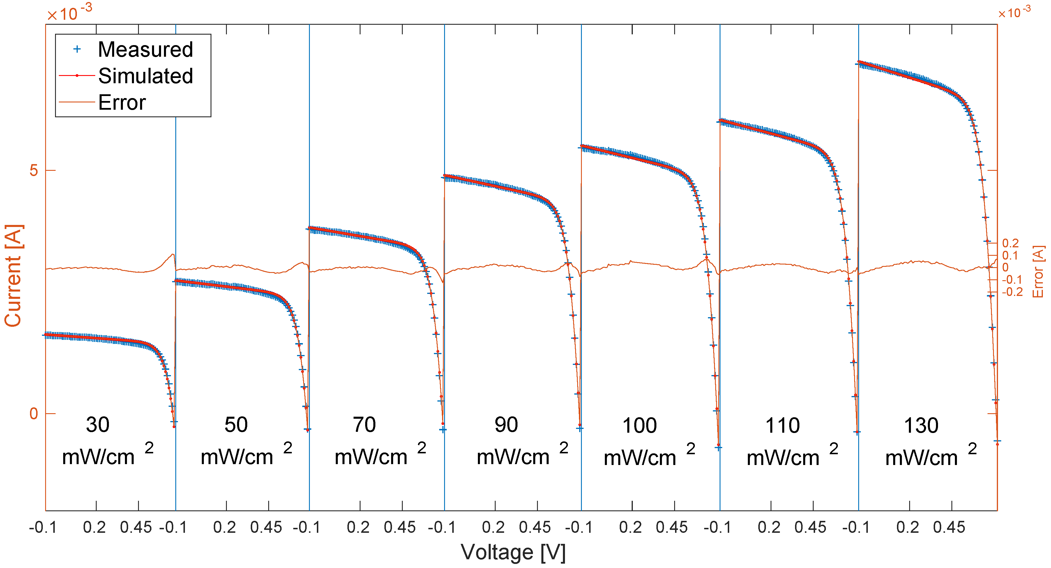
5. Validation of the Proposed Model on a Further Measurement Set

In order to verify that the model developed is not only valid for the single group of devices used for its definition (belonging to the same built set), but is in general valid for CIGS cells produced following the process described in Section 2, further tests where performed: in particular, the same measurement procedure described before was repeated for ten solar cell devices. The choice of irradiance range (from 30 mW/cm2–130 mW/cm2) and temperature range (from 25–50 °C) was made in order to consider typical environmental conditions for operative solar cells. The characterization process followed the same approach described previously: a couple of current-voltage curves were used to identify the model parameters, and the error in estimation for all the operating conditions was evaluated. For all the devices used in this validation, the results were satisfactory. Indeed, the mean squared error between simulated and measured values for the whole set of measurements was always below 1 × 10⁻⁸ and exactly between 1.8 × 10⁻⁹ and 7.7 × 10⁻⁹. In the two Figure 12 and Figure 13, we report the comparison, between measured and simulated values for all the available current-voltage curves, at different irradiance and temperatures of a single device. The device belongs to the validation set (i.e., was not previously used during the development of the model). This is done for the sake of simplicity, but analogous results were achieved for all the validation tests.
Lastly, the model was validated with irradiances and temperatures both outside SRC, to simulate real environmental conditions for which the two quantities can vary independently. Three notable tests are reported in Figure 14.
Both the irradiance and temperature influence on the performance were predicted with a remarkable accuracy, and consequently, we can affirm that this simple circuital model, with respect the other present in the literature, such as [10,11], can be used to evaluate electric yield for CIGS solar cells.

6. Conclusions

In conclusion, we proposed an experimental study of the dependence of the lumped circuital parameters of the one-diode model on atmospheric conditions, i.e., irradiance and temperature in the case of thin-film solar cells. Starting from two sets of experimental data obtained from Cu(In,Ga)Se2 solar cells fabricated by the LTPED technique, the lumped circuital parameters have been found. In order to obtain an accurate identification, a reduced form approach of the one-diode model has been adopted. It was possible to elaborate a comprehensive model for irradiance and temperature dependence, i.e., suitable relations describing the behavior of the parameters as functions of the environmental conditions. The set of introduced formulas was effective and allowed the prediction of the current-voltage characteristics for different environmental conditions outside SRC. An important strength of the proposed model is that the identification of the involved parameters can be achieved by using a few measured curves. Consequently, this can be considered a further step towards the development of a tailored PV simulator for CIGS-based modules. As a final consideration, it can be seen that the the high ideality factor obtained from the model identification suggests recombination phenomena. To account for this phenomena, a more complex model, the two-diode model, could be used. Investigating the temperature and irradiance dependence of the two-diode model is a very challenging open problem, for which we believe this work can be a good starting point.

Author Contributions

Experimental methodology and materials, L.C., M.B., A.D.I. and S.R. Experimental measurements, V.L. and M.R. Data analysis and model development, A.L. and G.M.L.

Funding

This research received no external funding.

Conflicts of Interest

The authors declare no conflict of interest.

References

  1. Shafarman, W.N.; Siebentritt, S.; Stolt, L. Cu(InGa)Se2 Solar Cells. In Handbook of Photovoltaic Science and Engineering; John Wiley & Sons, Ltd.: Hoboken, NJ, USA, 2011; pp. 546–599. [Google Scholar] [CrossRef]
  2. Liu, J.; Zhuang, D.; Luan, H.; Cao, M.; Xie, M.; Li, X. Preparation of Cu(In,Ga)Se2 thin film by sputtering from Cu(In,Ga)Se2 quaternary target. Prog. Nat. Sci. Mater. Int. 2013, 23, 133–138. [Google Scholar] [CrossRef]
  3. Salomé, P.M.; Fjällström, V.; Szaniawski, P.; Leitao, J.P.; Hultqvist, A.; Fernandes, P.A.; Teixeira, J.P.; Falcao, B.P.; Zimmermann, U.; da Cunha, A.F.; et al. A comparison between thin film solar cells made from co-evaporated CuIn1−xGaxSe2 using a one-stage process versus a three-stage process. Prog. Photovolt. Res. Appl. 2015, 23, 470–478. [Google Scholar] [CrossRef]
  4. Paul, S.; Lopez, R.; Repins, I.L.; Li, J.V. Study of charge transport properties in a ZnO/CdS/Cu (In, Ga) Se2 solar cell via admittance spectroscopy. J. Vac. Sci. Technol. B Nanotechnol. Microelectron. Mater. Process. Meas. Phenom. 2018, 36, 022904. [Google Scholar] [CrossRef]
  5. Jackson, P.; Wuerz, R.; Hariskos, D.; Lotter, E.; Witte, W.; Powalla, M. Effects of heavy alkali elements in Cu(In,Ga)Se2 solar cells with efficiencies up to 22.6%. Phys. Status Solidi (RRL) Rapid Res. Lett. 2016, 10, 583–586. [Google Scholar] [CrossRef]
  6. Rampino, S.; Bissoli, F.; Gilioli, E.; Pattini, F. Growth of Cu(In,Ga)Se2 thin films by a novel single-stage route based on pulsed electron deposition. Prog. Photovolt. Res. Appl. 2013, 21, 588–594. [Google Scholar] [CrossRef]
  7. Mazzer, M.; Rampino, S.; Gombia, E.; Bronzoni, M.; Bissoli, F.; Pattini, F.; Calicchio, M.; Kingma, A.; Annoni, F.; Calestani, D.; et al. Progress on low-temperature pulsed electron deposition of CuInGaSe2 solar cells. Energies 2016, 9, 207. [Google Scholar] [CrossRef]
  8. Haque, M.M.; Rahman, M.M.; Chowdhury, M.I.B. Current-voltage characteristics of CdS/CIGS thin film solar cells: An analytical approach. In Proceedings of the 2014 1st International Conference on Non Conventional Energy (ICONCE 2014), Kalyani, India, 16–17 January 2014; pp. 24–27. [Google Scholar] [CrossRef]
  9. Rahim, A.B.; Hasan, A.S.; Biswas, P.; Ullah, A.; Chowdhury, M.I.B. Analytical modeling of J-V characteristics of CIGS based thin film solar cell considering voltage and space dependent electric field in the absorber layer. In Proceedings of the 2015 International Conference on Advances in Electrical Engineering (ICAEE), Dhaka, Bangladesh, 17–19 December 2015; pp. 368–371. [Google Scholar] [CrossRef]
  10. Lee, K.S.; Chung, Y.D.; Park, N.M.; Cho, D.H.; Kim, K.H.; Kim, J.H.; Kim, S.J.; Kim, Y.H.; Noh, S.K. Analysis of the Current-voltage Curves of a Cu(In,Ga)Se2 Thin-film Solar Cell Measured at Different Irradiation Conditions. J. Opt. Soc. Korea 2010, 14, 321–325. [Google Scholar] [CrossRef]
  11. Sun, X.; Silverman, T.; Garris, R.; Deline, C.; Alam, M.A. An Illumination- and Temperature-Dependent Analytical Model for Copper Indium Gallium Diselenide (CIGS) Solar Cells. IEEE J. Photovolt. 2016, 6, 1298–1307. [Google Scholar] [CrossRef]
  12. Attivissimo, F.; Adamo, F.; Carullo, A.; Lanzolla, A.M.L.; Spertino, F.; Vallan, A. On the performance of the double-diode model in estimating the maximum power point for different photovoltaic technologies. Measurement 2013, 46, 3549–3559. [Google Scholar] [CrossRef]
  13. Parisi, A.; Curcio, L.; Rocca, V.; Stivala, S.; Cino, A.C.; Busacca, A.C.; Cipriani, G.; La Cascia, D.; Di Dio, V.; Miceli, R.; et al. Thin film CIGS solar cells, photovoltaic modules, and the problems of modeling. Int. J. Photoenergy 2013, 2013, 817424. [Google Scholar] [CrossRef]
  14. Werner, B.; KoŁodenny, W.; Prorok, M.; Dziedzic, A.; Żdanowicz, T. Electrical modeling of CIGS thin-film solar cells working in natural conditions. Sol. Energy Mater. Sol. Cells 2011, 95, 2583–2587. [Google Scholar] [CrossRef]
  15. Hishikawa, Y.; Tobita, H.; Sasaki, A.; Yamagoe, K.; Onuma, T.; Tsuno, Y. Current-voltage characteristics of novel PV devices under various irradiance and temperature conditions. In Proceedings of the 2013 IEEE 39th Photovoltaic Specialists Conference (PVSC), Tampa, FL, USA, 16–21 June 2013; pp. 1417–1422. [Google Scholar] [CrossRef]
  16. Atse, L.; de Waal Arjen, A.C.; Schropp, R.E.; Faaij, A.P.; van Sark, W.G. Comprehensive characterisation and analysis of PV module performance under real operating conditions. Prog. Photovolt. Res. Appl. 2017, 25, 218–232. [Google Scholar] [CrossRef]
  17. Gray, J.L. The Physics of the Solar Cell. In Handbook of Photovoltaic Science and Engineering; John Wiley & Sons, Ltd.: Hoboken, NJ, USA, 2005; pp. 61–112. [Google Scholar] [CrossRef]
  18. Soto, W.D.; Klein, S.; Beckman, W. Improvement and validation of a model for photovoltaic array performance. Sol. Energy 2006, 80, 78–88. [Google Scholar] [CrossRef] [Green Version]
  19. Laudani, A.; Fulginei, F.R.; Salvini, A. Identification of the one-diode model for photovoltaic modules from datasheet values. Sol. Energy 2014, 108, 432–446. [Google Scholar] [CrossRef]
  20. Laudani, A.; Riganti Fulginei, F.; Salvini, A.; Lozito, G.M.; Coco, S. Very fast and accurate procedure for the characterization of photovoltaic panels from datasheet information. Int. J. Photoenergy 2014, 2014, 946360. [Google Scholar] [CrossRef] [PubMed]
  21. Laudani, A.; Fulginei, F.R.; Salvini, A. High performing extraction procedure for the one-diode model of a photovoltaic panel from experimental I?V curves by using reduced forms. Sol. Energy 2014, 103, 316–326. [Google Scholar] [CrossRef]
  22. Laudani, A.; Fulginei, F.R.; Salvini, A.; Parisi, A.; Pernice, R.; Galluzzo, F.R.; Cino, A.C.; Busacca, A.C. One diode circuital model of light soaking phenomena in Dye-Sensitized Solar Cells. Opt. Int. J. Light Electron Opt. 2018, 156, 311–317. [Google Scholar] [CrossRef]
  23. Rampino, S.; Armani, N.; Bissoli, F.; Bronzoni, M.; Calestani, D.; Calicchio, M.; Delmonte, N.; Gilioli, E.; Gombia, E.; Mosca, R.; et al. 15% efficient Cu (In, Ga) Se2 solar cells obtained by low-temperature pulsed electron deposition. Appl. Phys. Lett. 2012, 101, 132107. [Google Scholar] [CrossRef]
  24. Paul, S.; Grover, S.; Repins, I.L.; Keyes, B.M.; Contreras, M.A.; Ramanathan, K.; Noufi, R.; Zhao, Z.; Liao, F.; Li, J.V. Analysis of Back-Contact Interface Recombination in Thin-Film Solar Cells. IEEE J. Photovolt. 2018, 8, 871–878. [Google Scholar] [CrossRef]
  25. Lindahl, J.; Keller, J.; Donzel-Gargand, O.; Szaniawski, P.; Edoff, M.; Törndahl, T. Deposition temperature induced conduction band changes in zinc tin oxide buffer layers for Cu (In, Ga) Se2 solar cells. Sol. Energy Mater. Sol. Cells 2016, 144, 684–690. [Google Scholar] [CrossRef]
  26. Carrasco, M.; Laudani, A.; Lozito, G.M.; Mancilla-David, F.; Riganti Fulginei, F.; Salvini, A. Low-Cost Solar Irradiance Sensing for PV Systems. Energies 2017, 10, 998. [Google Scholar] [CrossRef]
  27. Espinosa-Gavira, M.; Agüera-Pérez, A.; González de la Rosa, J.; Palomares-Salas, J.; Sierra-Fernández, J. An On-Line Low-Cost Irradiance Monitoring Network with Sub-Second Sampling Adapted to Small-Scale PV Systems. Sensors 2018, 18, 3405. [Google Scholar] [CrossRef] [PubMed]
  28. Faba, A.; Gaiotto, S.; Lozito, G.M. A novel technique for online monitoring of photovoltaic devices degradation. Sol. Energy 2017, 158, 520–527. [Google Scholar] [CrossRef]
  29. Öztürk, S.; Canver, M.; Çadırcı, I.; Ermiş, M. All SiC Grid-Connected PV Supply with HF Link MPPT Converter: System Design Methodology and Development of a 20 kHz, 25 kVA Prototype. Electronics 2018, 7, 85. [Google Scholar] [CrossRef]
  30. Laudani, A.; Lozito, G.M.; Lucaferri, V.; Radicioni, M.; Riganti Fulginei, F.; Salvini, A.; Coco, S. An analytical approach for maximum power point calculation for photovoltaic system. In Proceedings of the 2017 IEEE European Conference on Circuit Theory and Design (ECCTD), Catania, Italy, 4–6 September 2017; pp. 1–4. [Google Scholar]
  31. Liu, C.L.; Chen, J.H.; Liu, Y.H.; Yang, Z.Z. An asymmetrical fuzzy-logic-control-based MPPT algorithm for photovoltaic systems. Energies 2014, 7, 2177–2193. [Google Scholar] [CrossRef]
  32. Li, C.; Chen, Y.; Zhou, D.; Liu, J.; Zeng, J. A high-performance adaptive incremental conductance MPPT algorithm for photovoltaic systems. Energies 2016, 9, 288. [Google Scholar] [CrossRef]
  33. Yaden, M.F.; Melhaoui, M.; Gaamouche, R.; Hirech, K.; Baghaz, E.; Kassmi, K. Photovoltaic system equipped with digital command control and acquisition. Electronics 2013, 2, 192–211. [Google Scholar] [CrossRef]
Figure 1. Schematic representation of the architecture of the Cu(In,Ga)Se2 (CIGS)-based cell under study. CBD, Chemical Bath Deposition; LTPED, Low-Temperature Pulsed Electron Deposition.
Electronics 07 00324 g001
Figure 2. I-V characteristics of the CIGS solar cell at different temperatures.
Electronics 07 00324 g002
Figure 3. I-V characteristics of the CIGS cell for different irradiance values.
Electronics 07 00324 g003
Figure 4. Dark (0 mW/cm2 and 25 °C) vs. SRC (100 mW/cm2 and 25 °C) I-V characteristics of the CIGS cells.
Electronics 07 00324 g004
Figure 5. Irradiance [30, 130] mW/m2 dependence of the short-circuit current (left) and open-circuit voltage (right).
Electronics 07 00324 g005
Figure 6. Temperature [25, 55] °C dependence of the short-circuit current (left) and open-circuit voltage (right).
Electronics 07 00324 g006
Figure 7. Representative scheme of the equivalent circuit described by the one-diode model.
Electronics 07 00324 g007
Figure 8. Comparison between measured and simulated values (obtained by the proposed set of formulas) for all the available current voltage curves at different temperatures. Irradiance was fixed at 100 mW/cm2, and the temperature range was [25, 55] °C.
Electronics 07 00324 g008
Figure 9. Absolute error in logarithmic scale between the measured and simulated value for all datasets with different temperatures. Irradiance was fixed at 100 mW/cm2, and the temperature range was [25, 55] °C.
Electronics 07 00324 g009
Figure 10. Comparison between measured and simulated values (obtained by proposed set of formulas) for all the available current voltage curves at different irradiance. Temperature was fixed at 25 °C, and the irradiance range was [30, 130] mW/m2.
Electronics 07 00324 g010
Figure 11. Absolute error in logarithmic scale between measured and simulated values for all datasets with different irradiance. Temperature was fixed at 25 °C, and the irradiance range was [30, 130] mW/m2.
Electronics 07 00324 g011
Figure 12. Comparison between measured and simulated values (obtained by the proposed set of formulas) for all the available current voltage curves at different irradiance levels [30, 130] mW/m2 and a temperature of 25°C.
Electronics 07 00324 g012
Figure 13. Comparison between measured and simulated values (obtained by the proposed set of formulas) for all the available current voltage curves at different temperatures [25, 55] °C for an irradiance value of 100 mW/cm2.
Electronics 07 00324 g013
Figure 14. Comparison between measured and simulated values (obtained by the proposed set of formulas) for all the available current voltage curves at conditions outside SRC for both temperature and irradiance.
Electronics 07 00324 g014
Table 1. Photovoltaic parameters of CIGS cells measured under Standard Reference Conditions (SRC) ((*) measured under dark conditions).
ParameterMeasured Value
J i r r 27.4 ± 1.3 mA/cm2
V o c 0.686 ± 0.010 V
FF0.67 ± 0.02
η 12.6 ± 0.82%
R s h 135 kΩcm2 (*)
R s 12 Ωcm2 (*)
Table 2. Five parameters found vs. irradiance for a temperature of 25 °C.
50 mW/cm290 mW/cm2110 mW/cm2
I i r r (A)0.0033280.0062920.007516
I o (A)4.913 × 10−101.958 × 10−93.316 × 10−9
R s h (Ω)1.802 × 1031.077 × 1031.030 × 103
R s (Ω)3.6113.1533.342
n1.6181.7771.847
Table 3. Five parameters found vs. temperature for an irradiance of 100 mW/cm2.
25 °C40 °C55 °C
I i r r (A)0.0068400.0068480.006899
I o (A)1.018 × 10−99.904 × 10−91.771 × 10⁻⁷
R s h (Ω)92512431807
R s (Ω)3.8772.6062.882
n1.7291.7401.887
Table 4. MSE for different cases of study.
CaseMSE
Case 1 (30 °C–45 °C)3.0651 × 10⁻⁹
Case 2 (35 °C–55 °C)3.1132 × 10⁻⁹
Case 3 (25 °C–40 °C–55 °C)2.8143 × 10⁻⁹
Case 4 (complete dataset)2.7682 × 10⁻⁹
Table 5. MSE for different cases of study.
CaseMSE
Case 1 (30 mW/cm2–110 mW/cm2)3.8654 × 10−9
Case 2 (complete dataset)3.4023 × 10⁻⁹

