40 dB-Isolation, 1.85 dB-Insertion Loss Full CMOS SPDT Switch with Body-Floating Technique and Ultra-Small Active Matching Network Using On-Chip Solenoid Inductor for BLE Applications

 , ,
, , 
Abstract
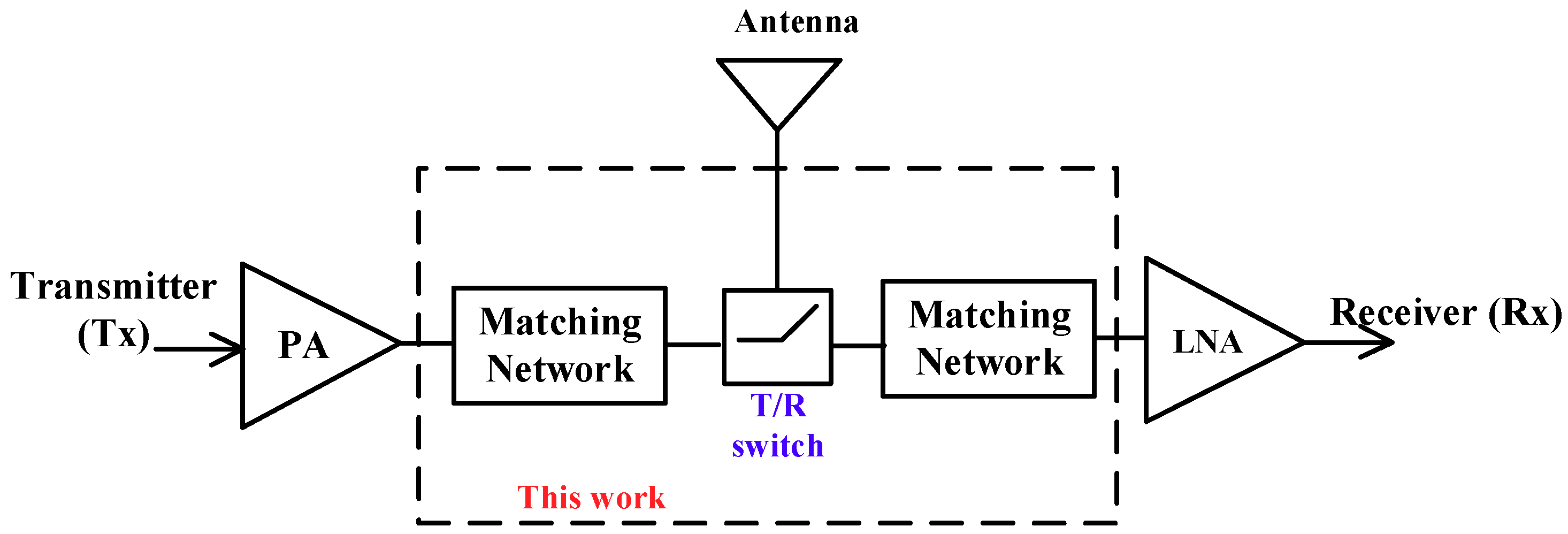
1. Introduction
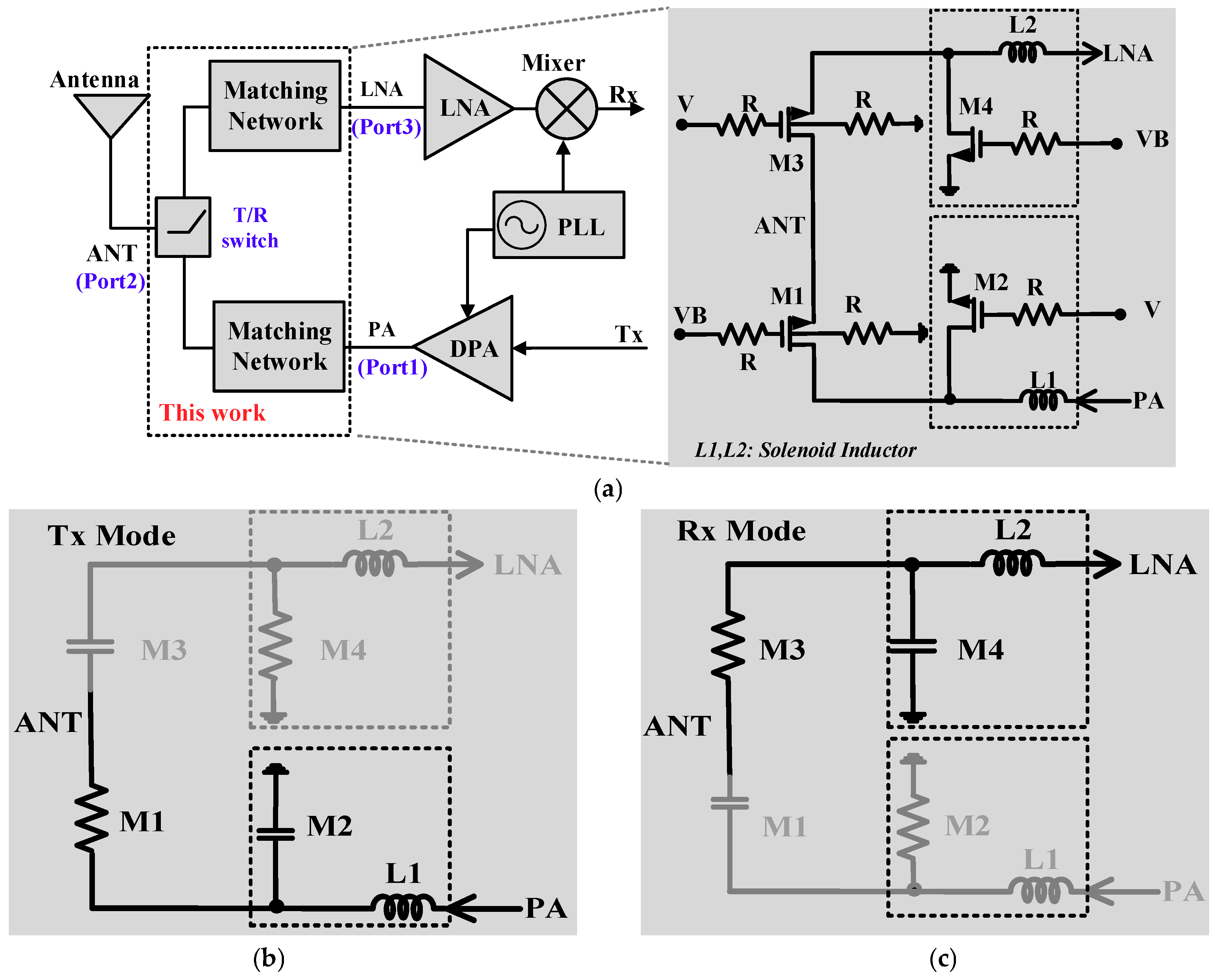
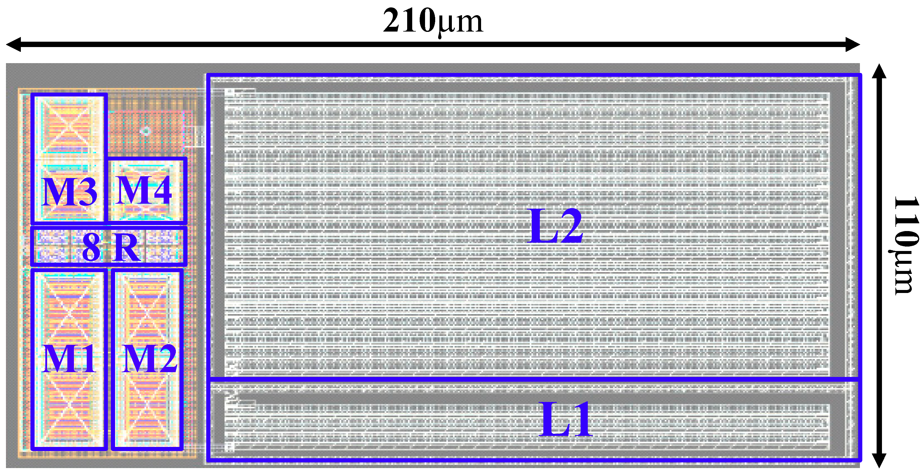
2. Circuits Implementation
2.1. SPDT Switch Circuit Design
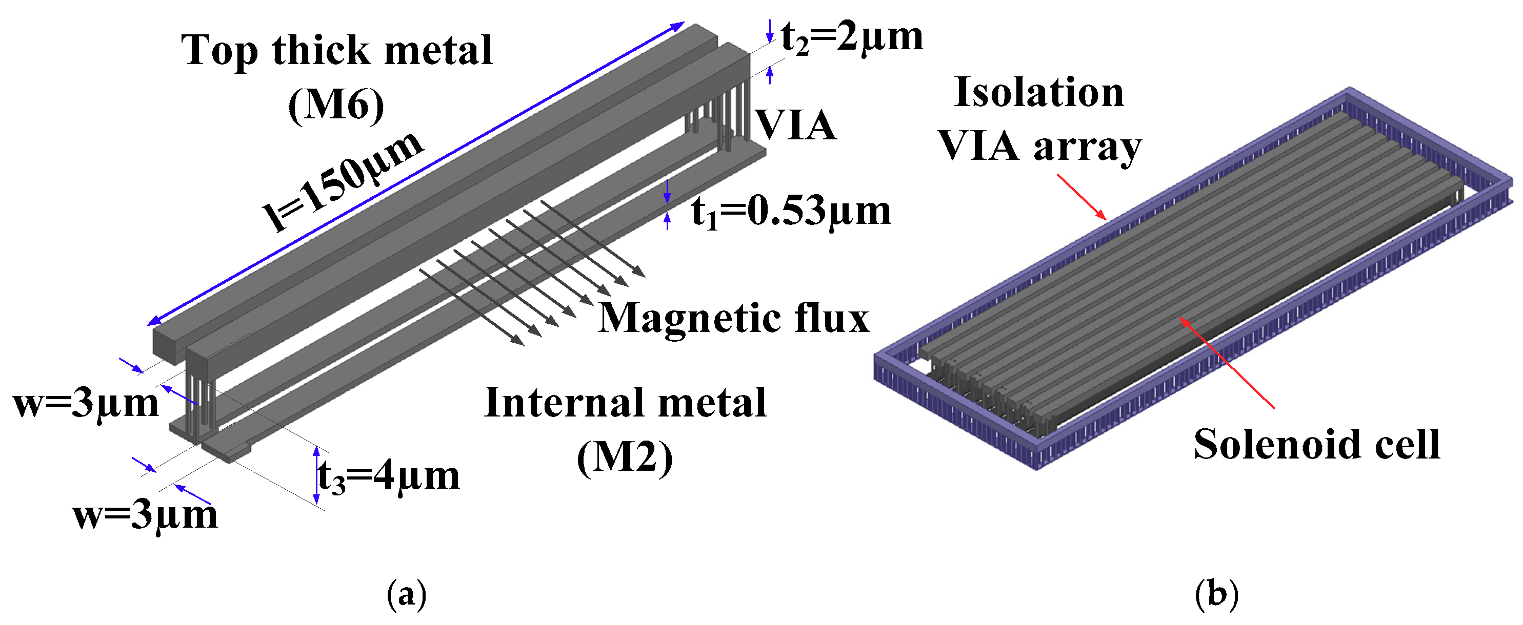
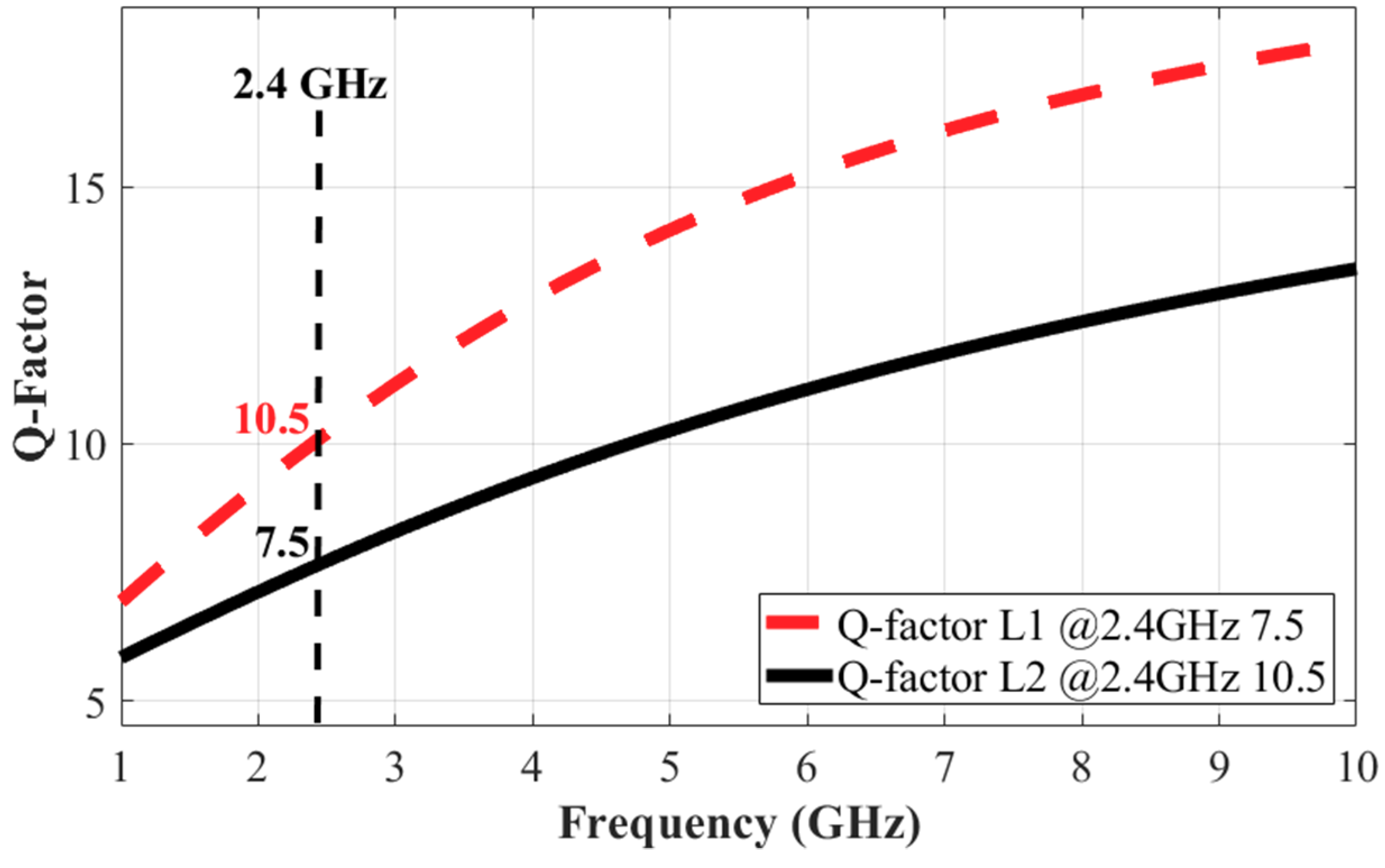
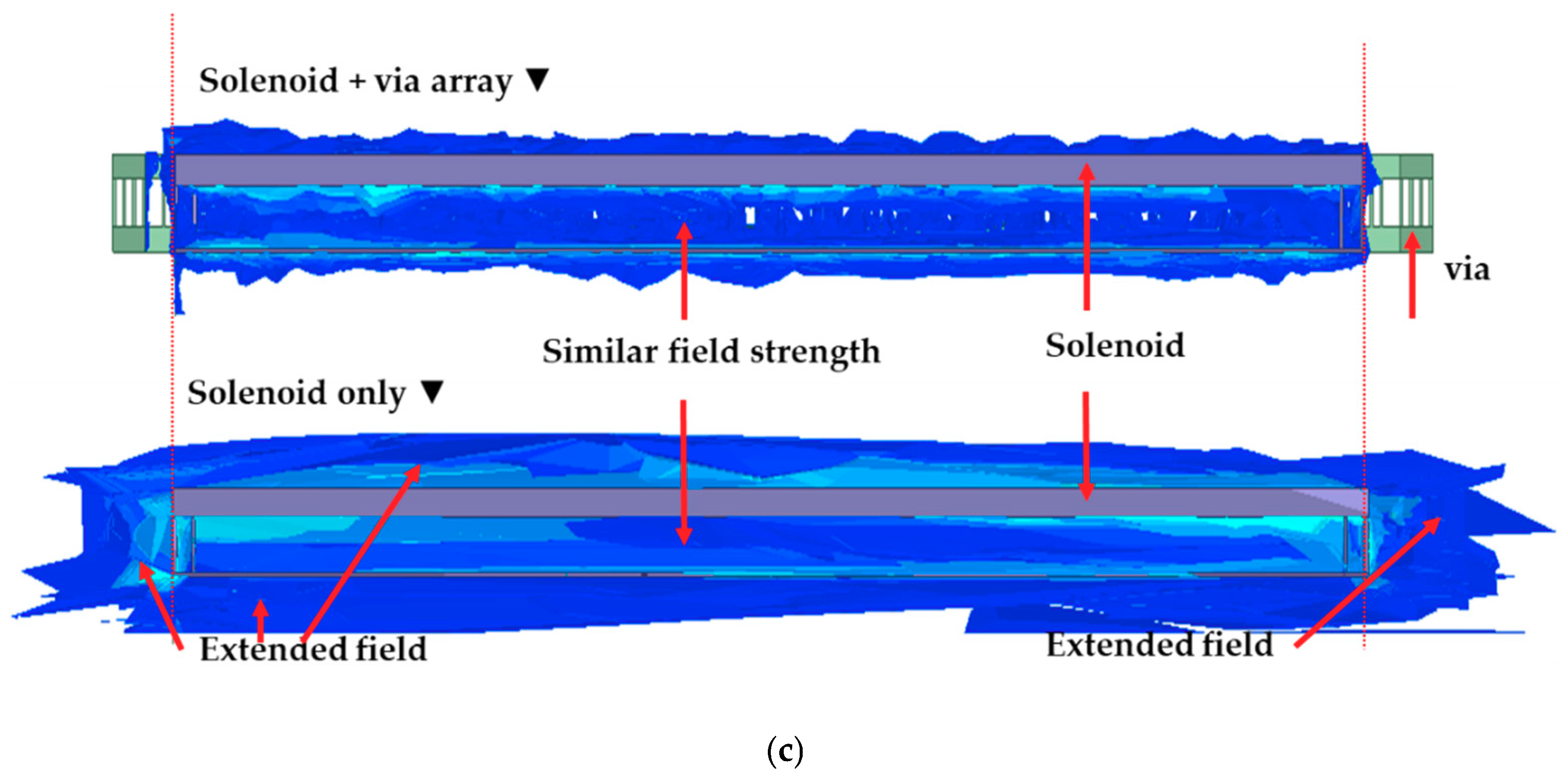
2.2. Solenoid Inductor Design
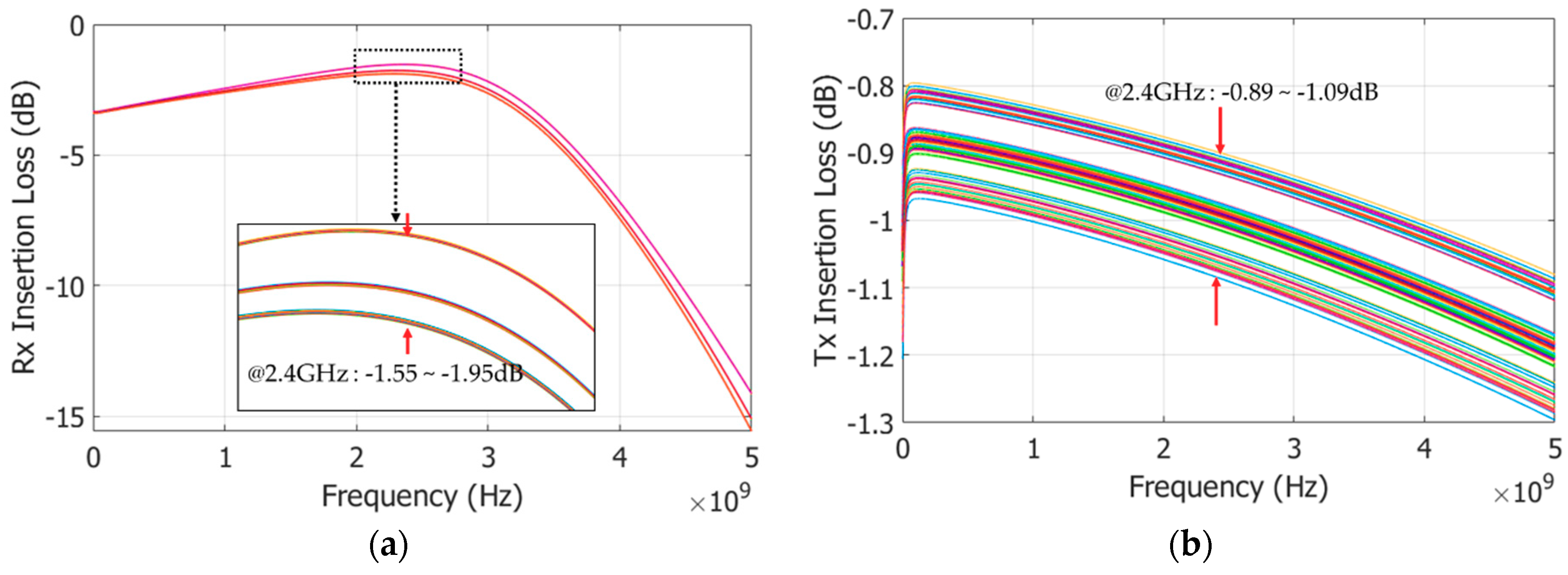
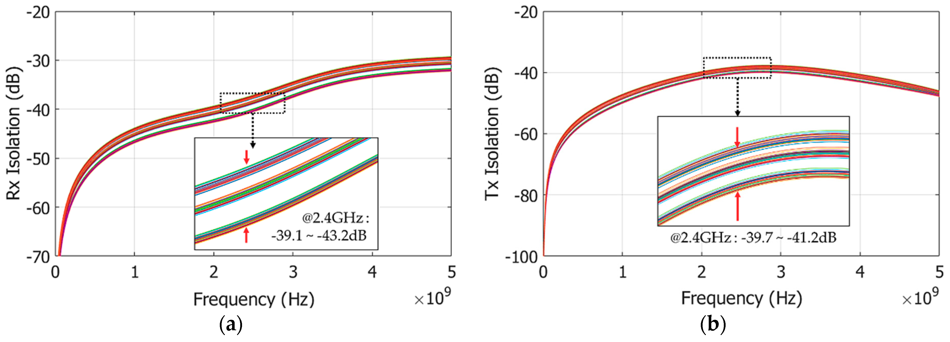
3. Results and Discussion
4. Conclusions
Author Contributions
Funding
Acknowledgments
Conflicts of Interest
References
- Peng, C.; Qian, K.; Wang, C. Design and Application of a VOC-Monitoring System Based on a ZigBee Wireless Sensor Network. IEEE Sens. J. 2015, 15, 2255–2268. [Google Scholar] [CrossRef]
- Han, J.; Choi, C.; Lee, I. More efficient home energy management system based on ZigBee communication and infrared remote controls. IEEE Trans. Consum. Electron. 2011, 57, 85–89. [Google Scholar]
- Xiao, Y.; Cui, Y.; Savolainen, P.; Siekkinen, M.; Wang, A.; Yang, L.; Ylä-Jääski, A.; Tarkoma, S. Modeling Energy Consumption of Data Transmission over Wi-Fi. IEEE Trans. Mob. Comput. 2014, 13, 1760–1773. [Google Scholar] [CrossRef]
- Yu, H.; Cheung, H.M.; Huang, L.; Huang, J. Power-Delay Tradeoff with Predictive Scheduling in Integrated Cellular and Wi-Fi Networks. IEEE J. Sel. Areas Commun. 2016, 34, 735–742. [Google Scholar] [CrossRef]
- Ensworth, J.F.; Reynolds, M.S. BLE-Backscatter: Ultralow-Power IoT Nodes Compatible with Bluetooth 4.0 Low Energy (BLE) Smartphones and Tablets. IEEE Trans. Microwave Theory Tech. 2017, 65, 3360–3368. [Google Scholar] [CrossRef]
- Jeon, W.S.; Dwijaksara, M.H.; Jeong, D.G. Performance Analysis of Neighbor Discovery Process in Bluetooth Low-Energy Networks. IEEE Trans. Veh. Technol. 2017, 66, 1865–1871. [Google Scholar] [CrossRef]
- Liang, Z.; Li, B.; Huang, M.; Zheng, Y.; Ye, H.; Xu, K.; Deng, F. A Low Cost BLE Transceiver with RX Matching Network Reusing PA Load Inductor for WSNs Applications. Sensors 2017, 17, 895. [Google Scholar] [CrossRef] [PubMed]
- Hou, B.; Chen, H.; Wang, Z.; Mo, J.; Chen, J.; Yu, F.; Wang, W. A 11 mW 2.4 GHz 0.18 µm CMOS Transceivers for Wireless Sensor Networks. Sensors 2017, 17, 223. [Google Scholar] [CrossRef] [PubMed]
- Park, S.; Lee, J.-Y.; Lee, J.-Y.; Yang, J.-R.; Beak, D. 25–34 GHz Single-Pole, Double-Throw CMOS Switches for a Ka-Band Phased-Array Transceiver. Appl. Sci. 2018, 8, 196. [Google Scholar] [CrossRef]
- Papotto, G.; Carrara, F.; Finocchiaro, A.; Palmisano, G. A 90-nm CMOS 5-Mbps Crystal-Less RF-Powered Transceiver for Wireless Sensor Network Nodes. IEEE J. Solid-State Circuits 2014, 49, 335–346. [Google Scholar] [CrossRef]
- Kawano, T.; Goto, K.; Ishihara, T. Asymptotic solution with higher-order terms for scattered fields by an impedance discontinuity of a planar impedance surface. In Proceedings of the 2011 IEEE International Symposium on Antennas and Propagation (APSURSI), Spokane, WA, USA, 3–8 July 2011; pp. 2503–2506. [Google Scholar]
- Cetindogan, B.; Ustundag, B.; Turkmen, E.; Wietstruck, M.; Kaynak, M.; Gurbuz, Y. A D-Band SPDT Switch Utilizing Reverse-Saturated SiGe HBTs for Dicke-Radiometers. In Proceedings of the German Microwave Conference (GeMiC), Freiburg, Germany, 12–14 March 2018. [Google Scholar]
- Lee, D.; Oh, S.J.; Kim, S.J.; Lee, C.H.; Song, C.H.; Kim, J.; Kim, W.S.; Kim, H.; Yoo, S.-S.; Hong, S.; et al. Low Power FSK Transceiver using ADPLL with direct modulation and integrated SPDT for BLE Application. In Proceedings of the 2016 IEEE Asian Solid-State Circuits Conference (A-SSCC), Toyama, Japan, 7–9 November 2016. [Google Scholar]
- Thome, F.; Ture, E.; Brückner, P.; Quay, R.; Ambacher, O. W-band SPDT switches in planar and tri-gate 100-nm gate-length GaN-HEMT technology. In Proceedings of the German Microwave Conference (GeMiC), Freiburg, Germany, 12–14 March 2018. [Google Scholar]
- Ulusoy, A.Ç.; Song, P.; Schmid, R.L.; Khan, W.T.; Kaynak, M.; Tillack, B.; Papapolymerou, J.; Cressler, J.D. A Low-Loss and High Isolation D-Band SPDT Switch Utilizing Deep-Saturated SiGe HBTs. IEEE Microwave Wireless Compon. Lett. 2014, 24, 400–402. [Google Scholar] [CrossRef]
- Sun, P.; Liu, P. Analysis of parasitic effects in triple-well CMOS SPDT switch. Electron. Lett. 2013, 49, 706–708. [Google Scholar] [CrossRef]
- Yeo, S.K.; Won, Y.S. X-band high-power HEMT SPDT switch with selectively anodised aluminum substrate. Electron. Lett. 2010, 46, 1627–1629. [Google Scholar] [CrossRef]
- Cheng, S.; Rantakari, P.; Malmqvist, R.; Samuelsson, C.; Vaha-Heikkila, T.; Rydberg, A.; Varis, J. Switched Beam Antenna Based on RF MEMS SPDT Switch on Quartz Substrate. IEEE Antennas Wirel. Propag. Lett. 2009, 8, 383–386. [Google Scholar] [CrossRef]
- Davulcu, M.; Özeren, E.; Kaynak, M.; Gurbuz, Y. A New 5–13 GHz Slow-Wave SPDT Switch with Reverse-Saturated SiGe HBTs. IEEE Microwave Wirel. Compon. Lett. 2017, 27, 581–583. [Google Scholar] [CrossRef]
- Yeh, M.C.; Tsai, Z.M.; Liu, R.C.; Lin, K.Y.; Chang, Y.T.; Huei, W. Design and Analysis for a Miniature CMOS SPDT Switch Using Body-Floating Technique to Improve Power Performance. IEEE Trans. Microwave Theory Tech. 2006, 54, 31–39. [Google Scholar]
- Beinart, R.; Nazarian, S. Effects of External Electrical and Magnetic Fields on Pacemakers and Defibrillators: From Engineering Principles to Clinical Practice. Circulation 2013, 128, 2799–2809. [Google Scholar] [CrossRef] [PubMed]
- Truong, T.K.N.; Lee, D.S.; Lee, K.Y. A Low Insertion Loss, High Isolation Switch Based on Single Pole Double Throw for 2.4GHz BLE Applications. IEIE Trans. Smart Process. Comput. 2016, 5, 164–168. [Google Scholar] [CrossRef]


| Components | Value |
|---|---|
| M1 | 640/280 µm |
| M2 | 400/280 µm |
| M3 | 576/280 µm |
| M4 | 80/280 µm |
| R | 15 kΩ |
| L1 | 1.1 nH |
| L2 | 9.9 nH |
| Work | Size (mm) | Insertion Loss (dB) | Isolation (dB) | Freq. (GHz) | Process |
|---|---|---|---|---|---|
| [17] | 4.4 × 3.1 * | 1.3 | 20.3 | 9.5 | GaAs |
| [18] | 21 × 8 * | 0.32 | 31.2 | 24 | RFMEMS |
| [19] | 0.77 × 0.82 * | 2.5 | 32 | 5 | SiGe |
| [20] | 0.2 × 0.15 * | 1.1 | 27 | 5.8 | CMOS |
| This Work | 0.21 × 0.11 ** | 1.85 | 39.1 | 2.4 | CMOS |
© 2018 by the authors. Licensee MDPI, Basel, Switzerland. This article is an open access article distributed under the terms and conditions of the Creative Commons Attribution (CC BY) license (http://creativecommons.org/licenses/by/4.0/).
Share and Cite
Nga, T.T.K.; Lee, D.; Kim, S.; Lee, M.; Hwang, K.; Yang, Y.; Lee, K.-Y. 40 dB-Isolation, 1.85 dB-Insertion Loss Full CMOS SPDT Switch with Body-Floating Technique and Ultra-Small Active Matching Network Using On-Chip Solenoid Inductor for BLE Applications. Electronics 2018, 7, 297. https://doi.org/10.3390/electronics7110297
Nga TTK, Lee D, Kim S, Lee M, Hwang K, Yang Y, Lee K-Y. 40 dB-Isolation, 1.85 dB-Insertion Loss Full CMOS SPDT Switch with Body-Floating Technique and Ultra-Small Active Matching Network Using On-Chip Solenoid Inductor for BLE Applications. Electronics. 2018; 7(11):297. https://doi.org/10.3390/electronics7110297
Chicago/Turabian StyleNga, Truong Thi Kim, DongSoo Lee, SungJin Kim, Minjae Lee, KeumCheol Hwang, Youngoo Yang, and Kang-Yoon Lee. 2018. "40 dB-Isolation, 1.85 dB-Insertion Loss Full CMOS SPDT Switch with Body-Floating Technique and Ultra-Small Active Matching Network Using On-Chip Solenoid Inductor for BLE Applications" Electronics 7, no. 11: 297. https://doi.org/10.3390/electronics7110297
APA StyleNga, T. T. K., Lee, D., Kim, S., Lee, M., Hwang, K., Yang, Y., & Lee, K.-Y. (2018). 40 dB-Isolation, 1.85 dB-Insertion Loss Full CMOS SPDT Switch with Body-Floating Technique and Ultra-Small Active Matching Network Using On-Chip Solenoid Inductor for BLE Applications. Electronics, 7(11), 297. https://doi.org/10.3390/electronics7110297