Design and optimization of collection efficiency and conversion gain of buried p-well SOI pixel X-ray detector

Abstract
:1. Introduction
2. Pixel Structure
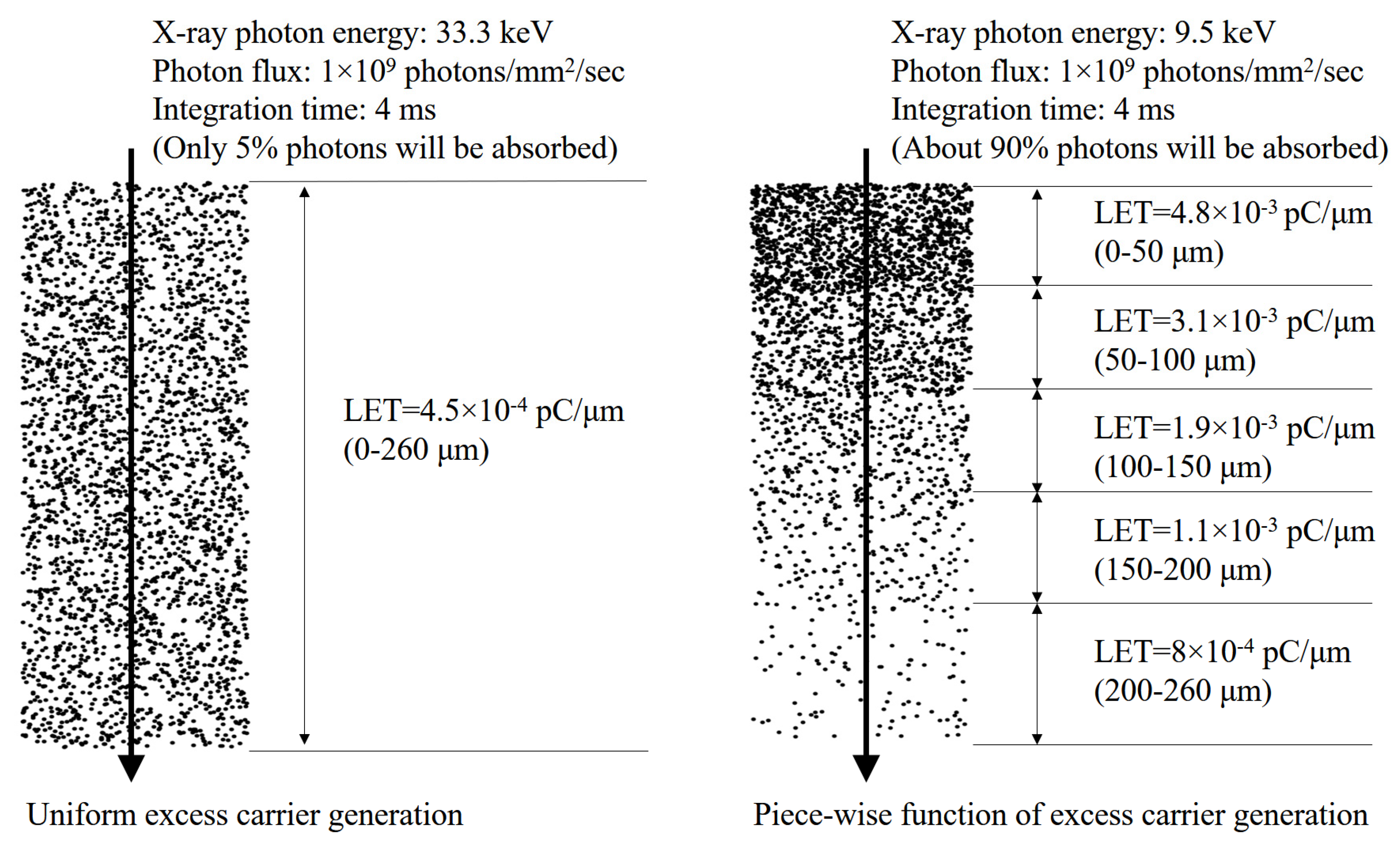
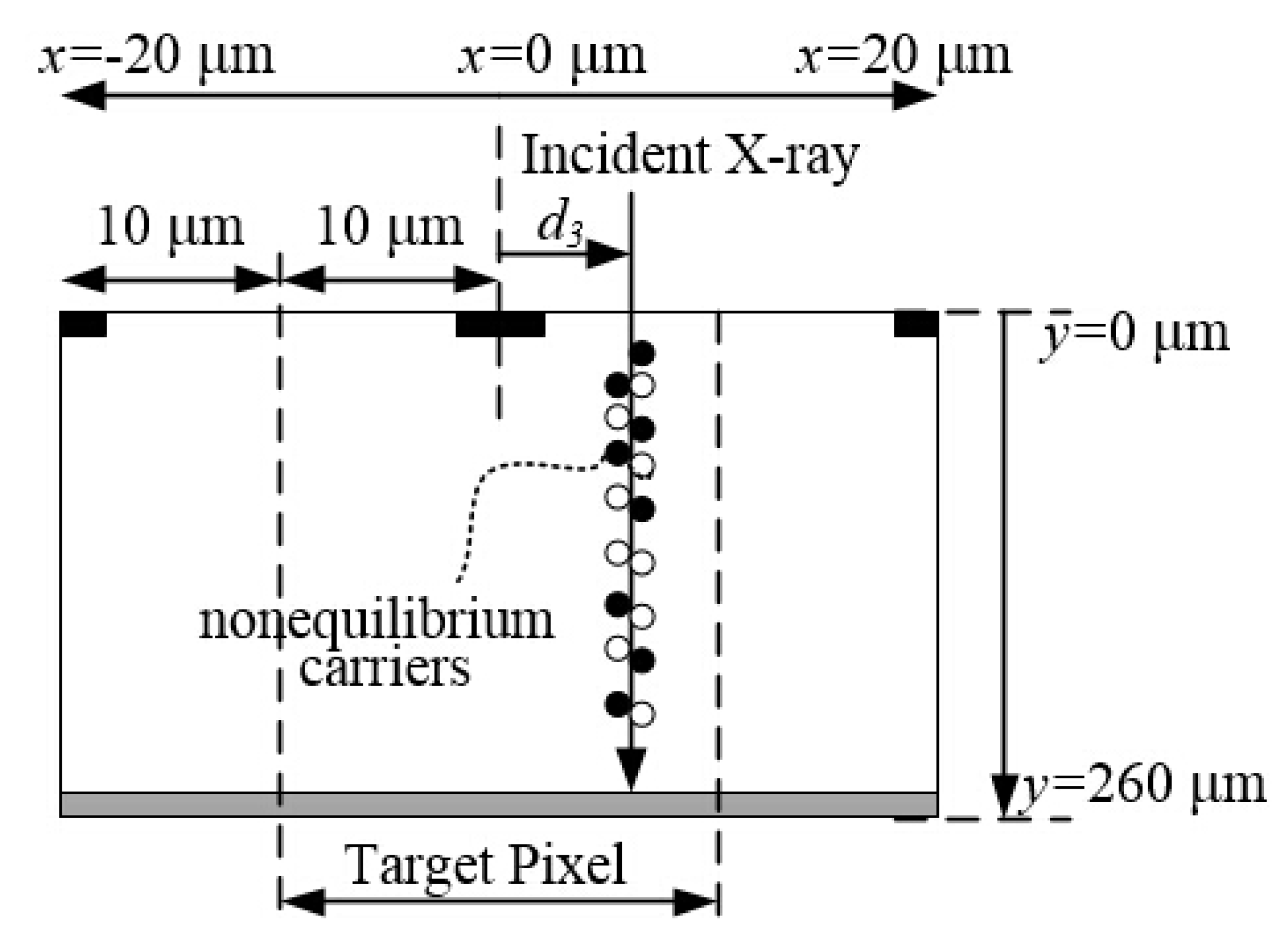
3. Incident X-ray Penetration Model
4. Simulation Results
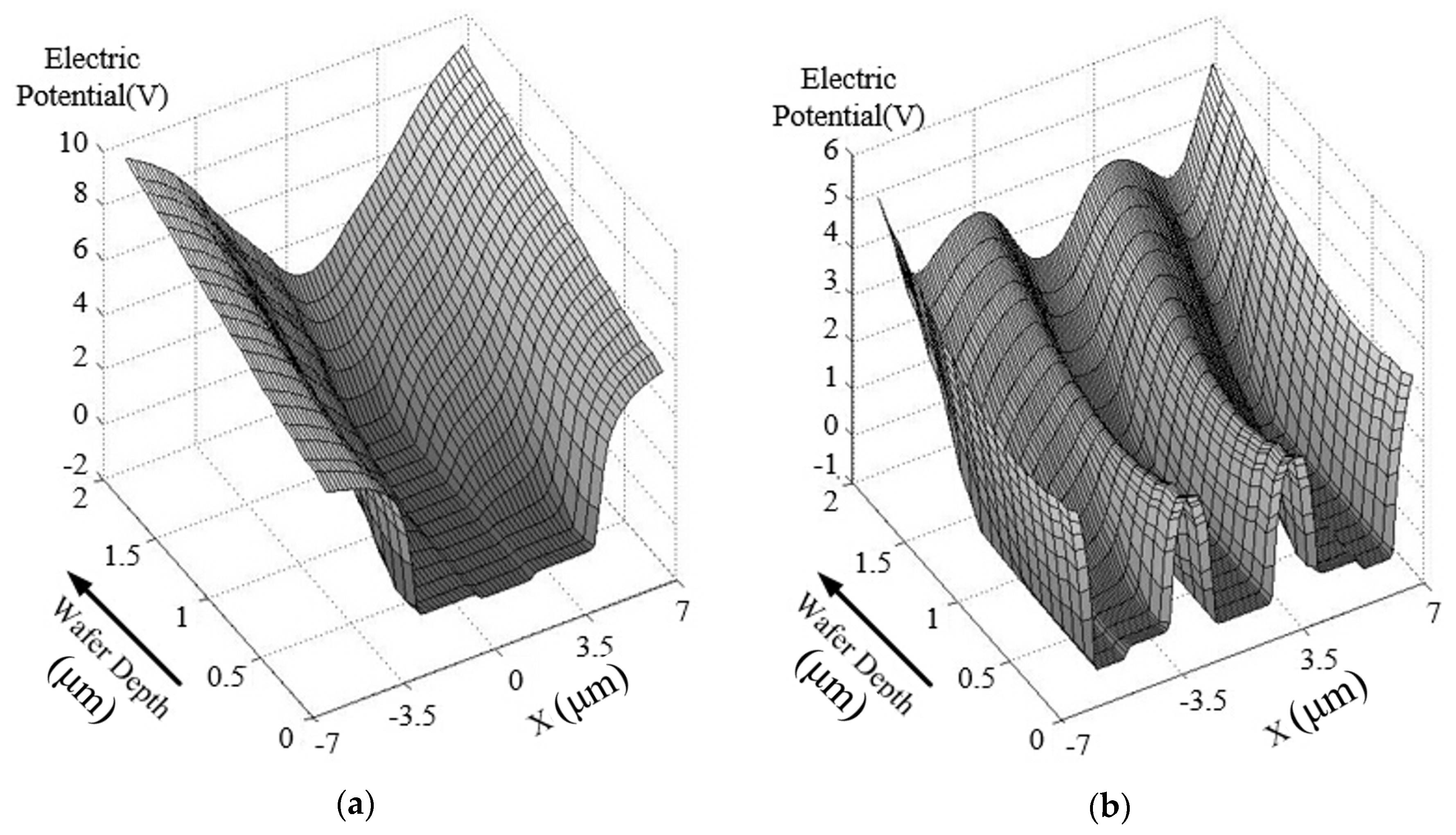
4.1. Electric Potential Distribution
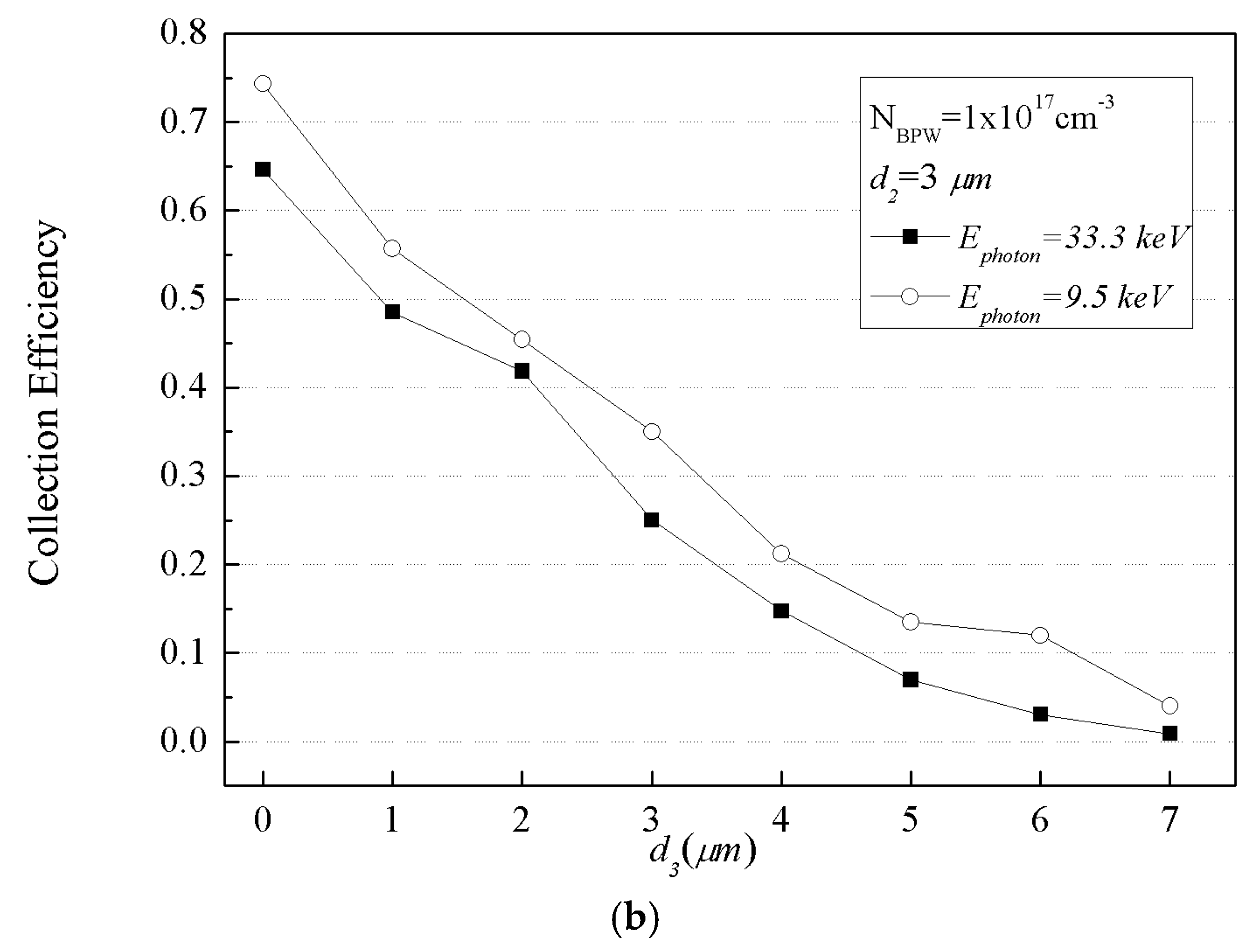
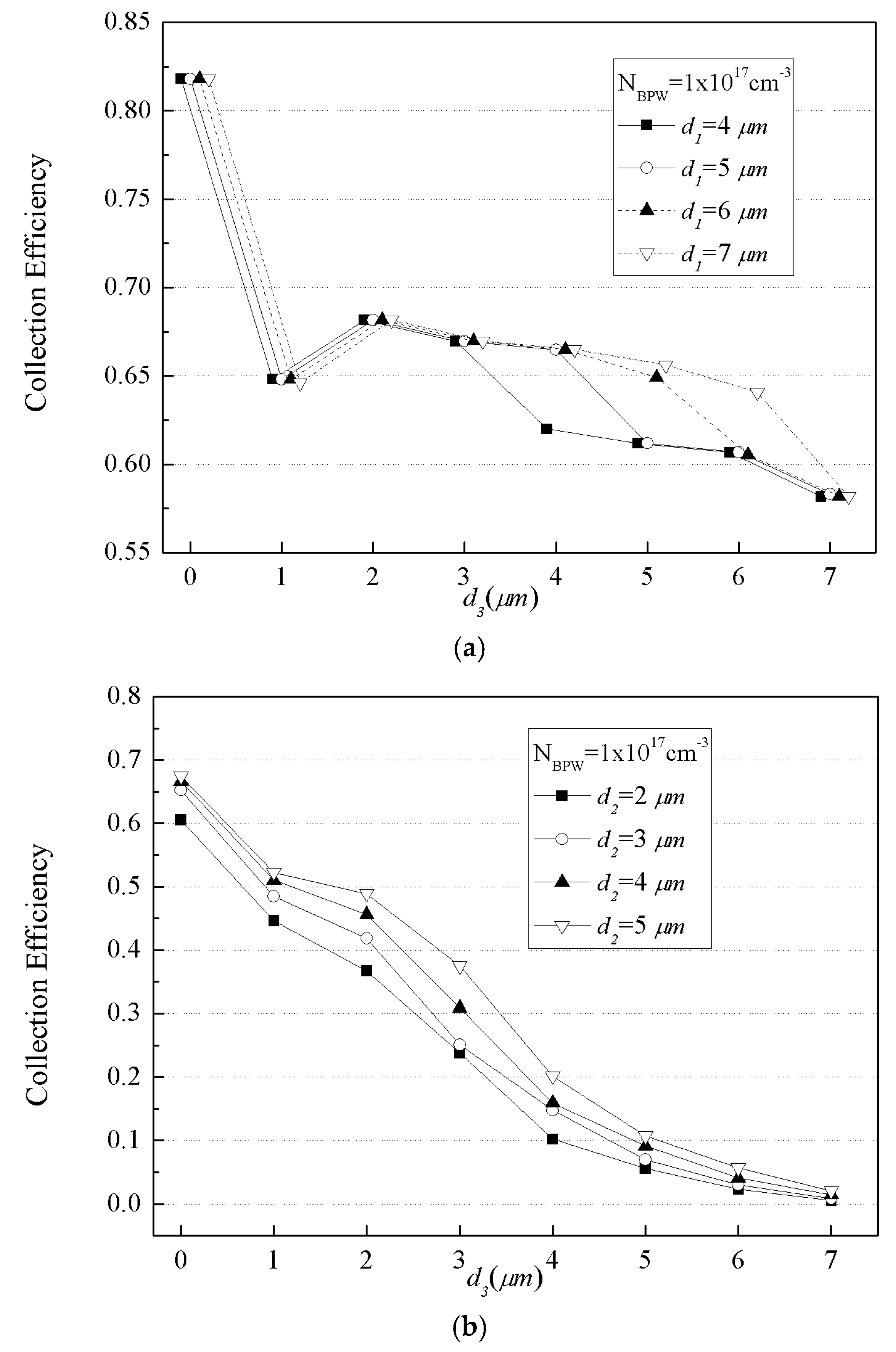
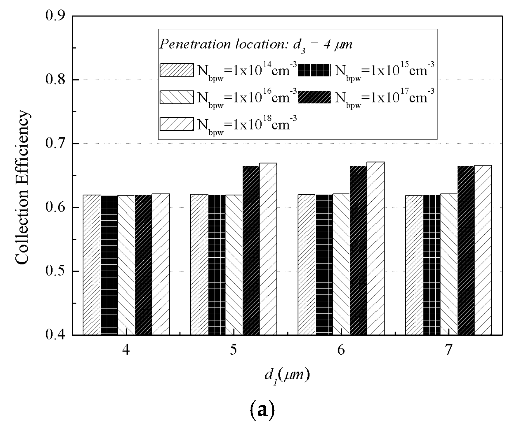
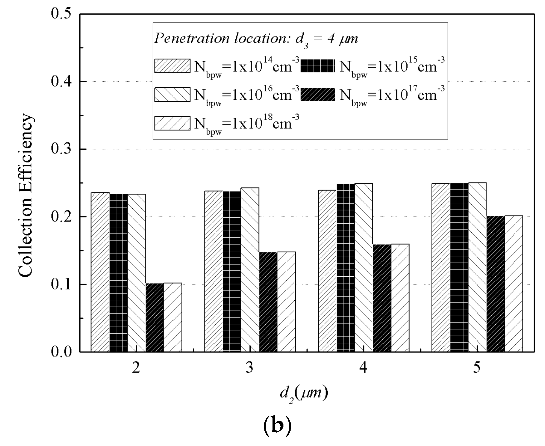
4.2. Carrier Collection Efficiency
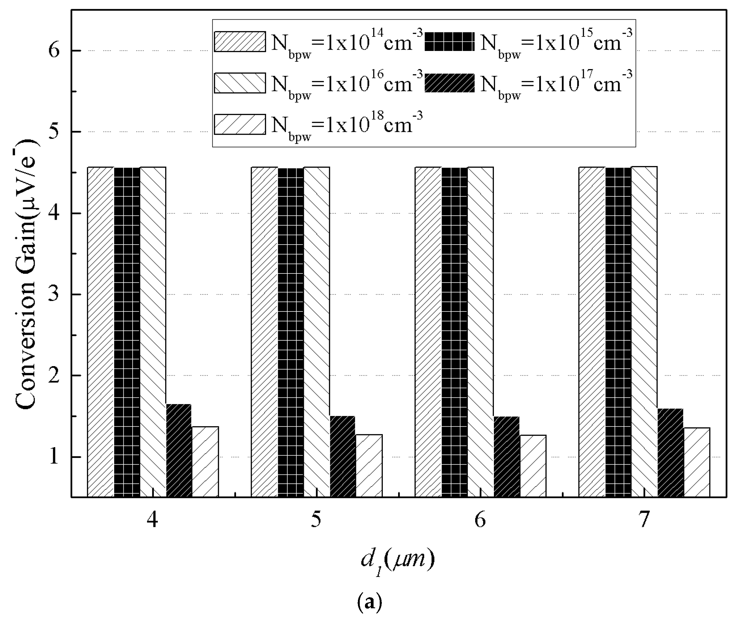
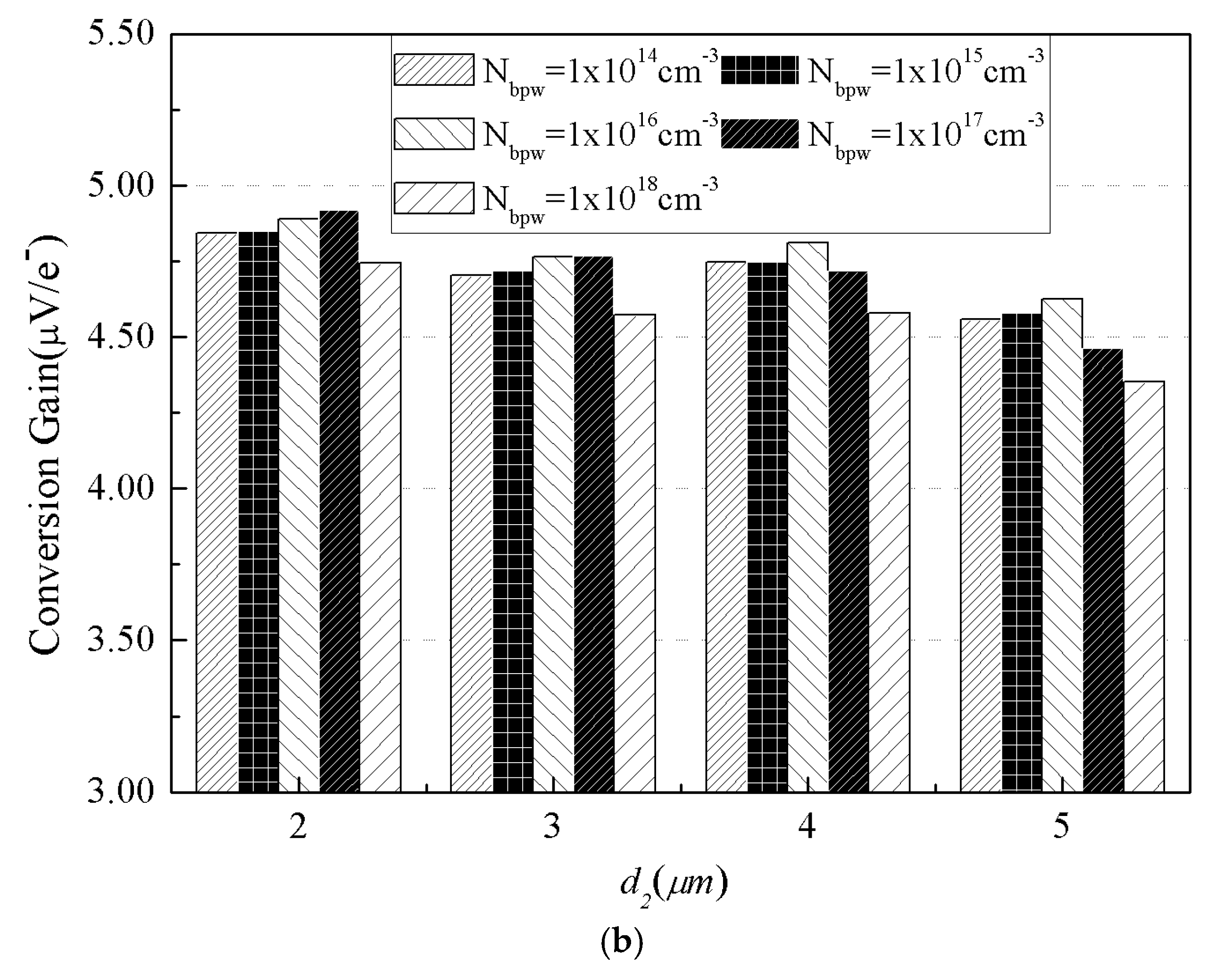
4.3. Conversion Gain
5. Conclusions
Acknowledgments
Author Contributions
Conflicts of Interest
References
- Seibert, J.A. One hundred years of medical diagnostic imaging technology. Health Phys. 1995, 69, 695–720. [Google Scholar] [CrossRef] [PubMed]
- Prekas, G.; Sabet, H.; Bhandari, H.H.; Derderian, G.; Robertson, F.; Kudrolli, H.; Stapels, C.; Christian, J.; Kleinfelder, S.; Cool, S.; et al. Direct and indirect detectors for X-ray photon counting systems. In Proceedings of the 2011 IEEE Nuclear Science Symposium and Medical Imaging Conference (NSS/MIC), Valencia, Spain, 23–29 October 2011; pp. 1487–1493. [Google Scholar]
- Seibert, J.A. X-ray Imaging Physics for Nuclear Medicine Technologists. Part 1: Basic Principles of X-ray Production. J. Nucl. Med. Technol. 2004, 32, 139–147. [Google Scholar] [PubMed]
- Overdick, M.; Bäumer, C.; Engel, K.J.; Fink, J.; Herrmann, C.; Kruger, H.; Simon, M.; Steadman, R.; Zeitler, G. Status of Direct Conversion Detectors for Medical Imaging With X-rays. IEEE Trans. Nucl. Sci. 2009, 56, 1800–1809. [Google Scholar] [CrossRef]
- Ryu, S.G.; Tsuru, T.G.; Nakashima, S.; Takeda, A.; Arai, Y.; Miyoshi, T.; Ichimiya, R.; Hironori, I.; Matsumoto, H.; Imamura, T.; et al. First Performance Evaluation of an X-ray SOI Pixel Sensor for Imaging Spectroscopy and Intra-Pixel Trigger. IEEE Trans. Nucl. Sci. 2011, 58, 2528–2536. [Google Scholar] [CrossRef]
- Miyoshi, T.; Arai, Y.; Hirose, M.; Ichimiya, R.; Ikemoto, Y.; Kohriki, T.; Tsuboyama, T.; Unno, Y. Performance study of SOI monolithic pixel detectors for X-ray application. Nucl. Instrum. Methods 2011, 636, S237–S241. [Google Scholar] [CrossRef]
- Hideaki, M.; Takeshi, G.T.; Takaaki, T.; Shinya, N.; Syukyo, G.R.; Ayaki, T.; Yasuo, A.; Toshinobu, M. Investigation of charge-collection efficiency of Kyoto’s X-ray astronomical SOI pixel sensors, XRPIX. Nucl. Instrum. Methods 2014, 765, 183–186. [Google Scholar]
- Tsuru, T.G.; Matsumura, H.; Takeda, A.; Tanaka, T.; Nakashima, S.; Arai, Y.; Mori, K.; Takenaka, R.; Nishioka, Y. Development and Performance of Kyoto’s X-ray Astronomical SOI pixel (SOIPIX) sensor. Proc. SPIE 2014, 9144. [Google Scholar] [CrossRef]
- Niemiec, H.; Jastrzab, M.; Kucewicz, W.; Kucharski, K.; Marczewski, J.; Sapor, M.; Tomaszewski, D. Full-size monolithic active pixel sensors in SOI technology-Design considerations, simulations and measurements results. Nucl. Instrum. Methods 2006, 568, 153–158. [Google Scholar] [CrossRef]
- Gregory, P.; Vyshnavi, S.; David, P.; Richard, F.; Steve, K.; Beverly, L.; Antonio, M.S.; Joel, V.; Marshall, B. Characterization of Three-Dimensional-Integrated Active Pixel Sensor for X-ray Detection. IEEE Trans. Electron. Devices 2009, 56, 2602–2611. [Google Scholar]
- Hu, Y.; Deptuch, G.; Turchetta, R.; Guo, C. A low-noise, low-power CMOS SOI readout front-end for silicon detector leakage current compensation with capability. IEEE Trans. Circuits. Syst. I Fundam. Theory Appl. 2001, 48, 1022–1030. [Google Scholar] [CrossRef]
- Tierno, J.A.; Rylyakov, A.V.; Friedman, D.J. A Wide Power Supply Range, Wide Tuning Range, All Static CMOS All Digital PLL in 65 nm SOI. IEEE J. Solid-State Circuits 2008, 43, 42–51. [Google Scholar] [CrossRef]
- Iwata, H.; Ohzone, T. Numerical analysis of alpha-particle-induced soft errors in SOI MOS devices. IEEE Trans. Electron. Devices 1992, 39, 1184–1190. [Google Scholar] [CrossRef]
- Marczewski, J.; Caccia, M.; Domanski, K.; Grabiec, P.; Grodner, M.; Jaroszewicz, B.; Klatka, T.; Kociubinski, A.; Koziel, M.; Kucewicz, W.; et al. Monolithic silicon pixel detectors in SOI technology. Nucl. Instrum. Methods 2005, 549, 112–116. [Google Scholar] [CrossRef]
- Schwantes, S.; Furthaler, J.; Schauwecker, B.; Dietz, F.; Graf, M.; Dudek, V. Analysis of the Back-Gate Effect on the on-State Breakdown Voltage of Smartpower SOI Devices. IEEE. Trans. Device Mater. Reliab. 2006, 6, 377–385. [Google Scholar] [CrossRef]
- Miyoshi, T. Recent progress in development of SOI pixel detectors. In Proceedings of the 2010 IEEE Nuclear Science Symposium Conference Record (NSS/MIC), 30 October–6 November 2010; pp. 1885–1888. [Google Scholar]
- Arai, Y.; Miyoshi, T.; Unno, Y.; Tsuboyama, T.; Terada, S.; Ikegami, Y.; Ichimiya, R.; Kohriki, T.; Tauchi, K.; Ikemoto, Y.; et al. Development of SOI pixel process technology. Nucl. Instrum. Methods 2011, 636, S31–S36. [Google Scholar] [CrossRef]
- Arai, Y.; Miyoshi, T.; Unno, Y.; Tsuboyama, T.; Terada, S.; Ikegami, Y.; Kohriki, T.; Tauch, K.; Ikemoto, Y.; Ichimiya, R.; et al. Developments of SOI monolithic pixel detectors. Nucl. Instrum. Methods 2010, 623, 186–188. [Google Scholar] [CrossRef]
- Toshinobu, M.; Yasuo, A.; Tadashi, C.; Yowichi, F.; Kazuhiko, H.; Shunsuke, H.; Yasushi, I.; Yoichi, I.; Yukiko, K.; Takash, K.; et al. Monolithic pixel detectors with 0.2 um FD-SOI pixel process technology. Nucl. Instrum. Methods 2013, 732, 530–534. [Google Scholar]
- Prigozhin, G.; Gendreau, K.; Bautz, M.W.; Burke, B.; Ricker, G. The depletion depth of high resistivity X-ray CCDs. IEEE Trans. Nucl. Sci. 1998, 45, 903–909. [Google Scholar] [CrossRef]
- Synopsys Inc. Guide, Sentaurus Device User, version E; Synopsys Inc.: Mountain View, CA, USA, 2010; pp. 489–498. [Google Scholar]
- Ryutaro, N.; Yasuo, A.; Toshinobu, M.; Keiichi, H.; Shunji, K.; Ryo, H. Development of an X-ray imaging system with SOI pixel detectors. Nucl. Instrum. Methods 2016, 831, 49–54. [Google Scholar] [CrossRef]
- Knoll, G.F. Radiation Detection and Measurement; John Wiley & Sons: Hoboken, NJ, USA, 2010; p. 390. [Google Scholar]
- Poudel, A.; McDermott, R.; Vavilov, M.G. Quantum efficiency of a microwave photon detector based on a current-biased Josephson junction. Phys. Rev. B 2012, 86, 174506. [Google Scholar] [CrossRef]
- Fossum, E.R. CMOS Image Sensors: Electronic Camera-on-a-Chip. IEEE Trans. Electron Devices 1995, 44, 1689–1698. [Google Scholar] [CrossRef]
- Li, W.; Xu, J.; Xu, C.; Li, B.; Yao, S. Collection efficiency and charge transfer optimization for a 4-T pixel with multi n-type implants. J. Semicond. 2011, 32, 124008. [Google Scholar] [CrossRef]
- Finger, G.; Beletic, J.W.; Dorn, R.; Meyer, M.; Mehrgan, L.; Moorwood, A.F.M.; Stegmeier, J. Conversion Gain and Interpixel Capacitance of Cmos Hybrid Focal Plane Arrays. Exp. Astron. 2006, 10, 135–147. [Google Scholar]


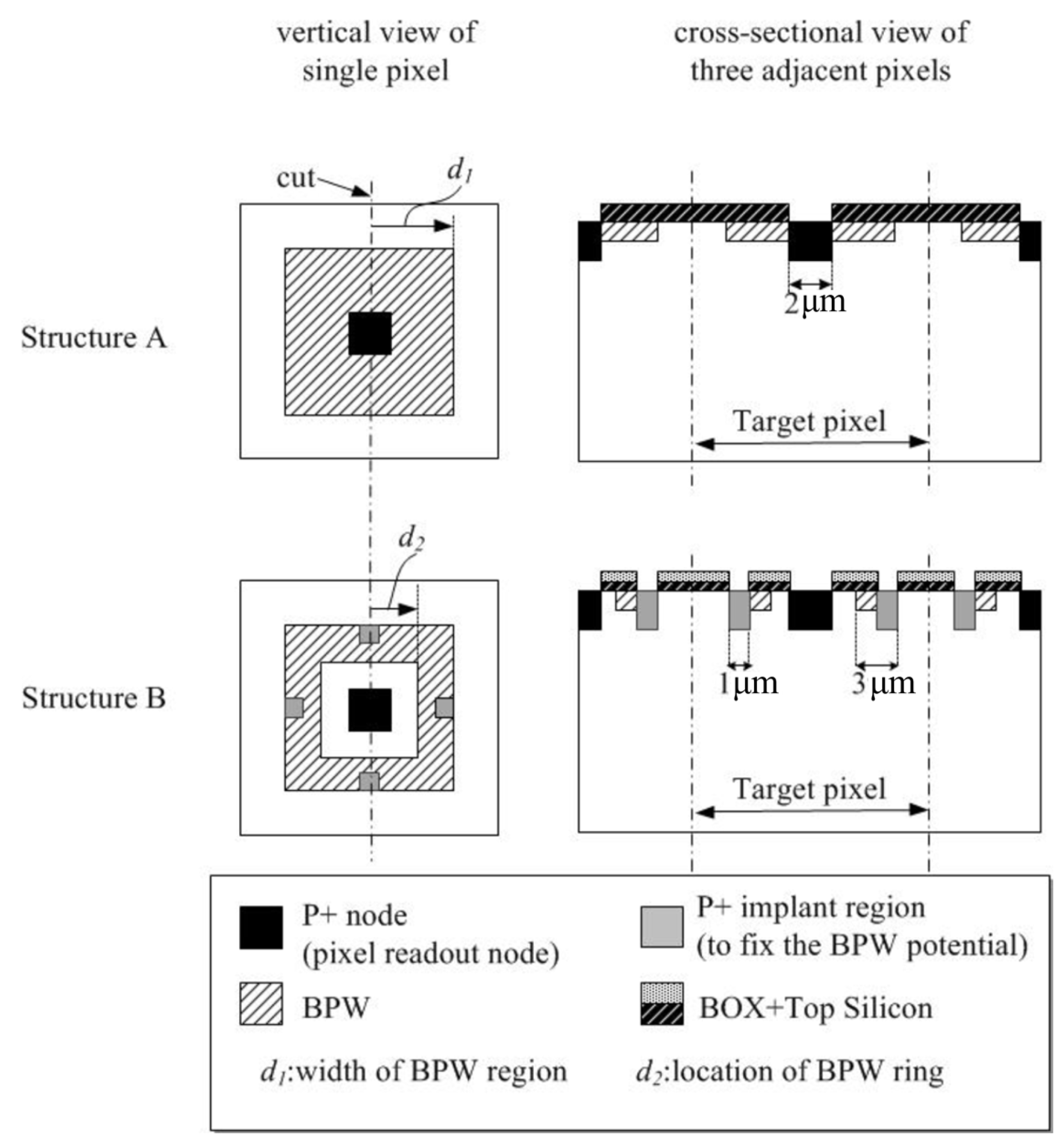
| Structure | Explanation |
|---|---|
| Structure A: pixel with extended BPW | The width of the extended BPW is (2 × d1) μm |
| Structure B: pixel with a BPW ring | BPW ring needs other additional P+ nodes to fix its potential; the width of the ring is 3 μm and the width of these four P+ nodes is 1 μm; the separation between the P+ node and the BPW ring is d2 μm. |
© 2017 by the authors. Licensee MDPI, Basel, Switzerland. This article is an open access article distributed under the terms and conditions of the Creative Commons Attribution (CC BY) license (http://creativecommons.org/licenses/by/4.0/).
Share and Cite
Shi, C.; Tian, L.; Feng, S.; Li, Q.; Wang, H. Design and optimization of collection efficiency and conversion gain of buried p-well SOI pixel X-ray detector. Electronics 2017, 6, 26. https://doi.org/10.3390/electronics6020026
Shi C, Tian L, Feng S, Li Q, Wang H. Design and optimization of collection efficiency and conversion gain of buried p-well SOI pixel X-ray detector. Electronics. 2017; 6(2):26. https://doi.org/10.3390/electronics6020026
Chicago/Turabian StyleShi, Chen, Li Tian, Songlin Feng, Qiliang Li, and Hui Wang. 2017. "Design and optimization of collection efficiency and conversion gain of buried p-well SOI pixel X-ray detector" Electronics 6, no. 2: 26. https://doi.org/10.3390/electronics6020026
APA StyleShi, C., Tian, L., Feng, S., Li, Q., & Wang, H. (2017). Design and optimization of collection efficiency and conversion gain of buried p-well SOI pixel X-ray detector. Electronics, 6(2), 26. https://doi.org/10.3390/electronics6020026