1. Introduction
As wave energy research enters a stage of offshore testing and operation, there is need for extensive on-site monitoring [
1]. In commercial offshore projects, there is also a growing interest for real-time monitoring to use for active control, forecasting and maintenance planning [
2]. Due to the tough offshore environment and the high costs for installation and maintenance [
3,
4], there are many aspects to be considered for the design of an offshore monitoring system.
At Uppsala University, Uppsala, Sweden, full scale offshore operation of wave power has been studied since 2006 [
5,
6]. The wave energy converters (WECs) considered, described in [
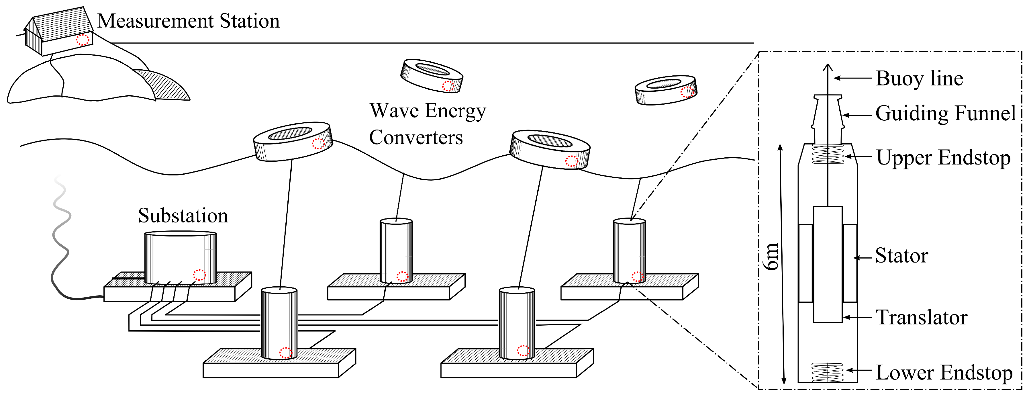
7], are of the point absorber type, which makes each unit limited in size and power production. Consequently, they are to be placed in bigger arrays, as illustrated in
Figure 1. Due to the relatively small and separate units, a distributed measurement system is needed, with equipment both onshore and offshore, and on both sea bed and sea surface. During ten years of offshore experiments at the Lysekil test site, on the west coast of Sweden, much knowledge and experience has been gained, not only regarding the studied WECs, but also regarding how to, or how not to, set up measurements and signal transmission. Important challenges have been identified, such as reliability, accessibility and data synchronisation. Earlier generator measurement systems used within the Lysekil project are presented in [
8,
9,
10,
11].
This paper concerns part of a larger project to build a new robust and cheap measurement system for offshore monitoring of wave power. The paper will focus on the measurements placed inside the generator.
1.1. Measurement Objective
For the first prototype, the objective was to measure voltage, current and translator position inside a three-phase generator, shown in
Figure 1. It is a direct driven permanent magnet linear generator with a stroke-length of 2 m, after which an upper and a lower endstop spring limits its movement. Being directly driven, the generator produces electricity which varies both in amplitude and frequency, with a typical frequency in the magnitude of 10 Hz and a rated voltage of around 300
at translator speed 0.7 m/s. The WECs are built for either three-phase alternating current (AC) output, directly from the linear generator, or with a direct current (DC) output, using a passive rectifier installed inside the generator. The WEC is connected to the measurement station, either directly (for a single WEC) or via the substation (which connects multiple WECs), as in
Figure 1. At the measurement station, the power can either be sent to the grid or to different passive or active loads used for research purposes.
The main use for voltage and current measurements inside the generator is power production monitoring, both in total and per phase, to evaluate the WEC’s power production and behavior at different sea states. Besides power production, monitoring the voltage and current in each phase can give useful indications of the operational status, such as mechanical stability in the generator [
12,
13,
14]. The translator position measurement was included for position and speed reference. Later on, a larger number of measurements will be added to the system, such as structural forces, thermal properties, air gap measurements, etc., all in order to study the generator operation in better detail. To keep the measurement system flexible for future adaptations, the design was kept modular with a separate unit for each measurement.
The measurement ranges were decided from generator specifications and from the wave climate at the offshore test site [
5]. The three-phase AC measurements required a range of ±1.2 kV and ±350 A. DC measurements required a range of 0–2 kV and 0–400 A. Considering the stroke length and installation procedure of the translator, a 4 m range was needed to measure its position from the bottom of the generator. The full measurement system, including the logger, was decided to have a bandwidth of 1 kHz. To ensure minimum damping and phase shift within this range, the cutoff frequency was set to around 10 kHz for the printed circuit boards (PCBs) developed. The data will later be post-processed with digital filters to remove high-frequency noise. A bandwidth of 1 kHz is well beyond the the need for the measurements implemented in this initial version, since the expected electrical frequency will be in the 10 Hz region. It is implemented, though, to enable more dynamic measurements in future versions of the measurement system.
1.2. Power Supply and Signal Transmission
Power supply and data acquisition for the measurment system is to be placed outside the generator. When possible, power will be provided by the substation, as illustrated in
Figure 1 and described in [
15], which interconnects the test site WECs and sends power and data onshore via cable. It offers both power supply and a NI CompactRio based data acquisition system [
16]. If substation connection is not an option, the measurement system will be powered by batteries. These batteries, together with data logging, will in such cases be placed in a retrievable pressure vessel next to the generator. The logger, especially designed for low power consumption, is based on an ATMEL328P micro controller. It samples eight channels at 1 kHz with a 16 bit resolution, using an ADS8345 analog-to-digital converter.
1.3. System Requirements
Low power consumption is essential in order to maximize battery operation time. A wide supply voltage range makes the measurement system flexible and robust. It is also important to limit the number of conductors running to and from the WEC, due to cost and availability of subsea cables and contacts.
After installation and final assembly of the generator, any changes, improvements or maintenance will become impossible. This makes reliability and robustness crucial. It is important that no voltage or current surges from the generator can damage the measurement system. The measurement system must also be mechanically robust and designed with consideration to its installation and operation inside the generator.
There are off-the-shelf products that meet the specifications stated for this measurement system, regarding accuracy, speed and robustness. There are also more sophisticated field-programmable gate array (FPGA)-based industrial control systems that offer a wide flexibility for both measurements and data acquisition and control [
17]. However, using such systems would require a combination of modules that together offer functionality, cost and power consumption far beyond what is actually needed for this application. In order to build a distributed measurement system that simultaneously monitors parameters in several generators and buoys during long term operation, the cost, complexity and power consumption of each measurement unit must be minimized.
1.4. Paper Layout
This paper will focus on design and testing of a measurement system to be placed inside a wave power generator. The method section describes design and function of the two developed measurement PCBs, as well as the experimental setup to test and evaluate their performance. It also describes how a three-phase measurement system, based on the developed PCBs, was built and tested in a linear wave power generator during onshore tests. PC-oscilloscope measurements were made in parallel, to use as reference for performance evaluation. The result section presents the performance and evaluation of the measurement system designed, based on both the PCB evaluation and the generator tests. This is followed by discussion and conclusion.
2. Method
To measure voltage and current, two separate PCBs were developed and tested. Each PCB will perform a bipolar measurement, of voltage or current, and output an analog signal suitable for 10–100 m transmission to the designated logger. The measurement must be galvanically isolated from the generator, noise resistant, robust and consume as little power as possible.
2.1. Choice of Key Components
A 4–20 mA signal carrier with a 12 mA zero offset was chosen for transmission between measurement system and logger. In addition, 4–20 mA signals are considered the industrial standard, favored for being simple, noiseproof and good for long distance communication. By using a two wire current loop transmitter,
XTR115 [
18], both power supply and current signal could be transmitted in the same conductor pair, which minimizes the number of cables. The chosen transmitter is especially suited for battery operation, with a wide input voltage range. It also provides a 5 V and a 2.5 V supplementary voltage supply, which was used to support other components on the low-voltage side of the circuit.
Hall effect sensors were chosen for current measurements, using
HAIS150-P and
HAIS200-P for AC and DC measurements respectively [
19]. This type of sensor has good accuracy, a wide input range and is not sensitive to over-currents and external interference [
19,
20]. The sensors allow for a ±450 A and ±600 A measurement range, with galvanic insulation up to 2500 V. For voltage sensing, an isolated amplifier,
amc1200 [
21], was chosen, which has a ±250 mV input range. A high galvanic isolation (4 k
), low noise and low non-linearity motivated the component choice. External voltage dividers were needed to scale the measurement range to the ±250 mV PCB input. The translator position measurement was made with a draw wire sensor,
MicroEpsilon WDS-5000-P115-PA-C [
22], combined with a voltage PCB unit.
2.2. PCB Layout
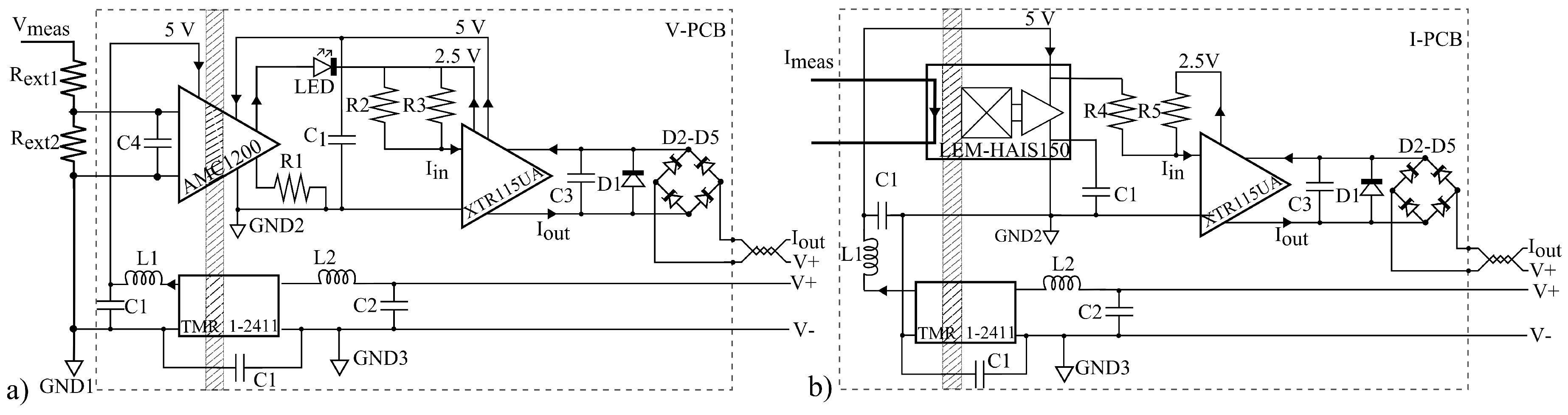
The two measurement circuits are presented in
Figure 2. It should be noted that some ancillary components have been left out to make the essential function of the circuits more approachable. Circuitry and components displayed outside the dotted lines are external to the PCB.
and
in
Figure 2a represent pre-PCB resistive voltage dividers and the circuitry to the right of the diode bridge represents signal and power supply cabling to the logger and battery unit.
2.2.1. Voltage PCB
Figure 2a presents the voltage measurement PCB. The galvanic isolation of the differential amplifier ensures that over-voltages from the generator are not transferred to the downstream circuitry. Along with this, a galvanic isolation barrier divides the PCB into a high voltage side (left) and a low voltage side (right), represented as striped areas in
Figure 2. A separate isolated DC/DC converter,
TMR 1-2411SM [
23], supplies the high voltage side. The low voltage side is driven by the current loop transmitter. In order to match the isolation amplifier output range (2.55 ± 2 V) to the current loop transmitter input range (40–200
A), the signal is scaled and shifted, using
,
and a
HLMP-K150 LED [
24]. The current loop transmitter amplifies the signal to 4–20 mA before leaving the PCB through a diode bridge, which enables bipolar voltage input.
The circuit layout seen in
Figure 2a gives the following transfer function:
is the common mode voltage from the differential amplifier,
is the differential amplifier gain,
is the input voltage signal,
is the forward voltage drop of the LED,
is the common mode voltage from the current loop transmitter and
is the current loop transmitter gain. The expected transfer function, when including component values, is presented in Equation (
2), stated in (mA/mV). It should be noted Equations (
1) and (
2) do not include the pre-PCB voltage dividers, since they are not part of the PCB. Including Equation (
3) will give the full transfer function:
2.2.2. Current PCB
Figure 2b presents the current measurement circuit. The circuit is much like the voltage measurement circuit, only changing the isolation amplifier for a current transducer. The generator output current is measured with Hall effect sensors which ensure galvanic isolation between the generator current and the measurement signal. Resistors
and
are used for balancing the current sensor output range (2.5 ± 1.875 V) to the current loop transmitter input range (40–200
A). The ±420–450 A input range for the AC measurements, and corresponding 570–600 A range for the DC measurements, was not transferred, since it was not within the required measurement range. Since the current loop transmitter could not provide enough power to support the current sensor, a separate DC/DC-converter was used, although not required for isolation like the voltage PCB circuit. The circuit layout seen in
Figure 2b gives the following transfer function:
where
is the common mode voltage from the current sensor,
is input current and
is the gain of the current sensor. The expected transfer functions for AC and DC measurements, when including component values, are presented in Equations (
5) and (
6), stated in (mA/A):
2.3. PCB Tests
To ensure stability, speed and signal transfer, the PCBs were tested for linearity, frequency response and step response. In addition, power consumption was measured for evaluation of operating time. In this section, the experimental setup for each test is described. A specification for the equipment and components used during the tests is found in
Table 1.
For all tests, the PCB output current signal was transferred through a 1.5 m signal cable and measured with an oscilloscope over a 500 Ω resistor. A 22 nF capacitor was connected in parallel, providing low pass filtering with a 14.5 kHz cutoff frequency. Input AC voltage was provided with a signal generator. Input current supply was provided, depending on the amount of current and type of signal needed, by (i) a signal generator; (ii) a lab power outlet (50 Hz); via a transformer or (iii) a DC supply. All resistors of significance where measured using a four terminal sensing method, in order to provide a more exact resistance (see
Table 1).
Voltage Linearity Test: The PCB input and output voltage was logged for a 0–250 mV AC input signal, applied in steps of 5 mV, over an 8 Ω input shunt resistor, the same model used for the generator measurement setup. Separate voltage dividers were used to scale down the input signal before entering the PCB. The linearity test was repeated for three different frequencies: 10 Hz, 100 Hz and 1 kHz. The test was also performed for both increasing and decreasing voltage levels, in order to test for any hysteresis effect.
Current Linearity Test: An input current in the range of 0–450 A was to be measured by the current sensor. By winding the signal carrying wire multiple turns through the current sensor, an up-scaling of 1:20 was achieved. Even so, no available signal generator could provide a sufficiently high current. Instead, a transformer and a 1 Ω power resistor was used to provide AC current directly from the lab power supply (at 50 Hz). The PCB input and output current signals were logged while stepping up the current by adding turns through the current sensor. It should be noted that the setup did not support tests at any other frequencies than 50 Hz. The step size was also limited. Since the current PCBs for AC and DC measurements are identical, with exception to the current sensor range, the tests were performed for only the AC version.
Voltage Frequency Response Test: The test setup used the same equipment as the voltage linearity test. The input amplitude was held fixed, while the frequency was varied in the range 1 Hz–100 kHz. For each step, the output signal and the phase shift between input and output signals were logged.
Current Frequency Response Test: An operational amplifier circuit was used to amplify the signal generator output. The circuit, using double operational amplifiers, was set up as suggested by data sheet recommendations [
25]. By looping the signal carrying wire multiple turns through the current sensor, a 30
current signal was obtained. The frequency was varied in the range of 1 Hz–100 kHz with the input current, measured as a voltage held constant over a 1 Ω power resistor. For each step, the output signal and the phase shift between input and output signals were logged.
Voltage Step Response Test: A signal generator was used to produce a square wave with 250 mV amplitude. Input and output signals were logged with a PC oscilloscope.
Current Step Response Test: A 6 A DC step was created with the help of a DC power supply and a 1 Ω power resistor. By winding the input signal wire multiple turns through the current sensor, a 120 A input signal was achieved, which is 25% of the full range. This method of scaling up the input current resulted in a slower time step, due to inductance. The chosen setup was a compromise between signal strength and rise time of the input step.
Power Consumption Test: During the PCB tests, the consumed current was measured with a multimeter, while the measurement system was fed with 24 V. The power consumption for the AC measurements was expected to be constant during both operation and standby. The two major consumers are the DC/DC converter, which provides a constant supply to either the operation amplifier or to the current sensor, and the current loop transmitter. The consumption of the current loop transmitter varies with the output current signal, but since it was designed to output 12 mA during standby and 12 ± 8 mA during operation, the average consumption should not vary with AC input signals. Thus, the measurement system consumption should be constant for AC measurements, which was also tested.
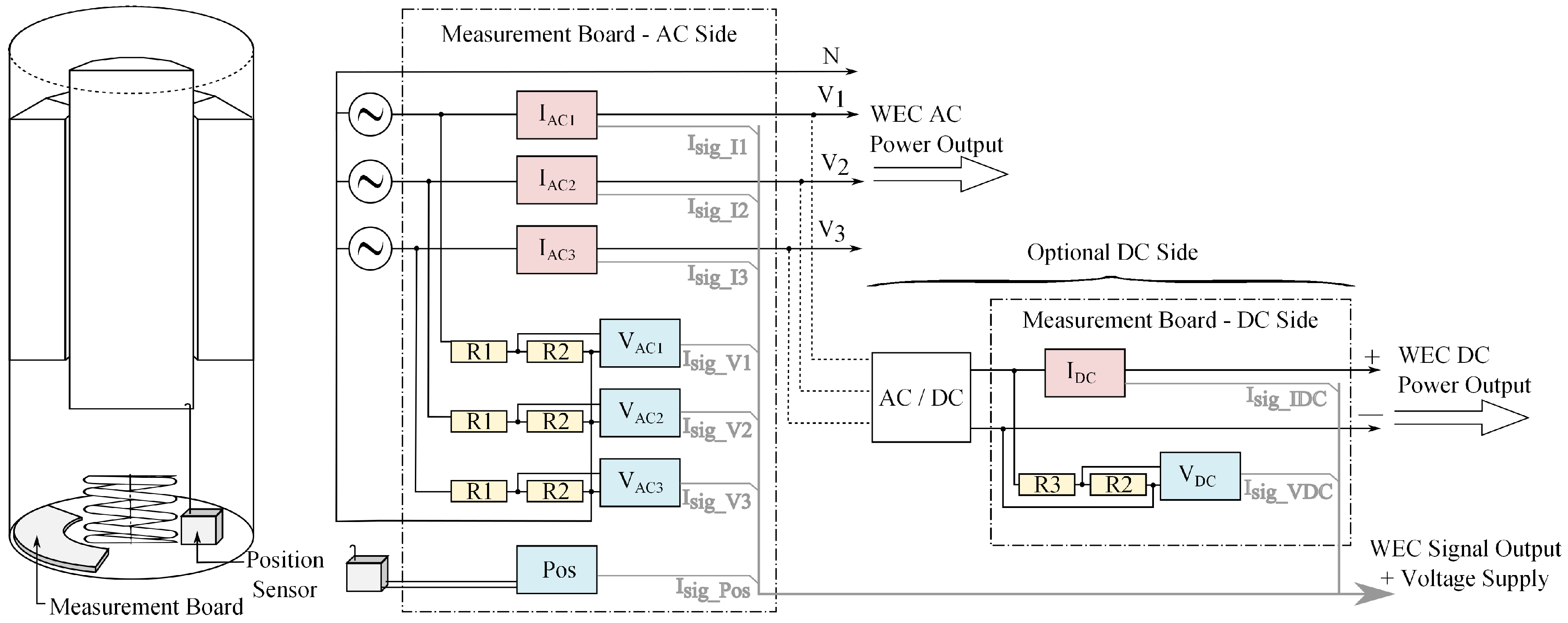
2.4. Generator Installation
Based on developed measurement PCBs, a full measurement system was built and installed in a wave power generator. It was a DC output generator, thus needing both AC and DC measurements.
Figure 3 shows a schematic of the placement of each measurement in relation to the generator, the passive rectifier and the WEC output. To facilitate the installation, all measurements were gathered on an isolated board, and installed in the bottom of the generator, also shown in
Figure 3. Each PCB was placed in an aluminum box for electromagnetic shielding. Shielded twisted pair cables were used to distribute power supply and signals, denoted
in the figure. The generator output voltage is scaled down via
R1-R3, with a factor 6.25k:1 for the AC voltage and 12.5k:1 for DC voltage, before entering the voltage measurement PCB. The choice of resistors,
VISHAY-RH050 [
26], was made based on the highest expected voltage, and thus heat dissipation, for each resistor, which were estimated to 1200 V and 15 W. To measure the translator position inside the generator a draw wire sensor,
MicroEpsilon WDS-5000-P115-PA-C, was used. It functions as a potentiometer, changing resistance as the wire is extended when the translator moves; the installation is depicted in
Figure 3. A voltage measurement PCB was used to facilitate the draw wire sensor, providing it with suitable voltage supply and sending the returning current signal.
Mounted inside the linear generator, the measurement system will operate in a dry, cool and pressurized (about 2 bar) nitrogen atmosphere. Each PCB is mounted in a custom made plastic holder in an aluminum box that offers both mechanical protection and electromagnetic shielding. The PCBs are sprayed with a silicon based coating and all cable inlets are equipped with rubber cable glands to add extra moisture protection.
2.5. Generator Test—Experimental Setup
After installation, the system was tested by driving the generator with an overhead crane while logging the generator AC output with the installed measurement system and with reference probes in parallel. During the tests, the generator was connected to a resistive load via the AC/DC converter.
The measurement system output signal was measured over a 500 Ω (0.1%) resistor and logged by a NI CompactRIO industrial controller, module NI9205. A 47 nF capacitor was placed in parallel with the resistor, providing a high frequency noise rejection with a 6.8 kHz cutoff frequency. The voltage reference measurements were made with differential probes, TESTEC TT-SI9001. The current reference measurements were made with current probes, Agilent 1146A. Both reference measurements were logged with a 12-bit PC oscilloscope, PicoScope 4424, with a 10 kHz sampling frequency. By using 16 bit enhanced sampling, an automatic moving average filtering was performed to raise the resolution by four bits. This gave an effective sampling rate of 39 Hz. This was sufficient, considering an expected electric frequency of 1 Hz for the generator output during these tests. Due to speed limitation in the crane, reaching approximately one tenth of the generator’s rated speed, and due to over-dimensioning in the measurement system, the signal strength in the generator measurements was low, as expected.
The measured signals were compared and validated against the reference measurements. Signal-to-Noise Ratio (SNR) values were calculated for the reference signals, the measurement output data and the filtered measurement output data. For filtering, a digital moving average filter, span 256 samples, was used to imitate the reference signal filtering in the PC oscilloscope. SNR values were calculated by separating signals from noise and using Equation (
7), where A is the RMS amplitude.
3. Results
3.1. PCB Tests—Results and Evaluation
Figure 4 shows the finalized PCBs for voltage and current measurement. The PCBs are mounted inside protective aluminum boxes. The current current sensor protudes on the backside of the box lid which the current PCB is mounted on, not seen in the picture.
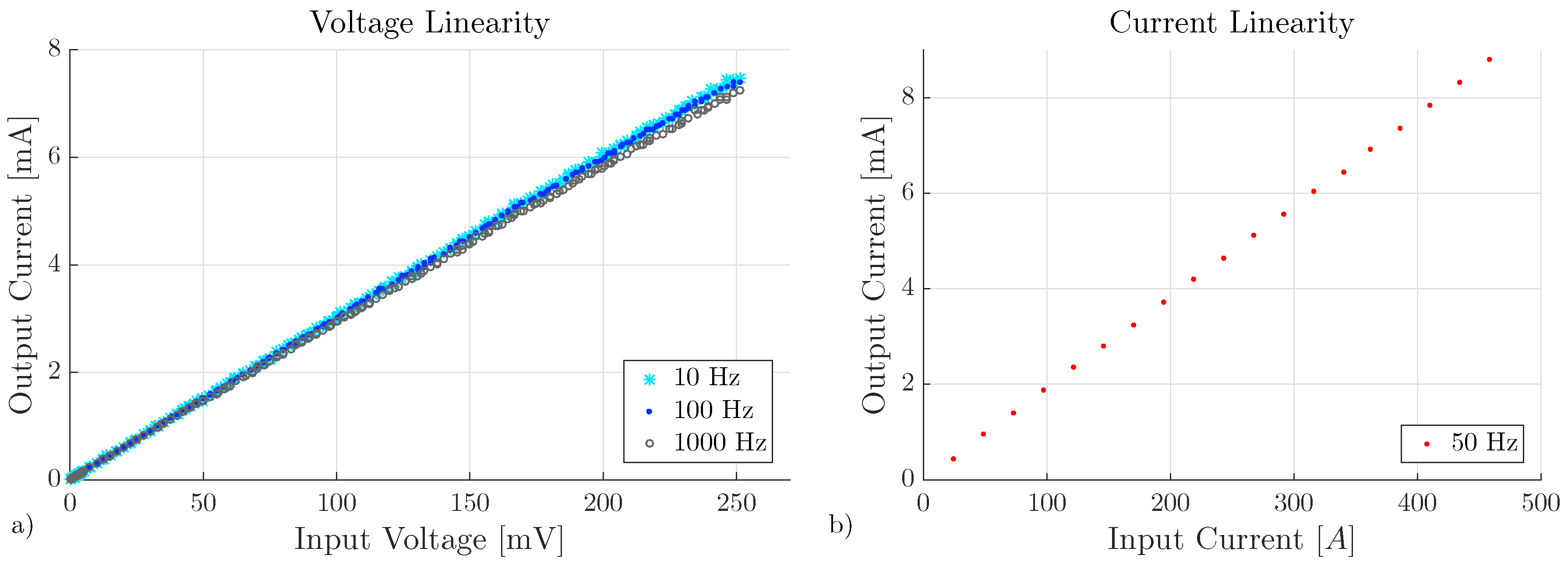
3.1.1. Linearity
Figure 5 shows the PCBs’ input/output linearity within the measurement range. Note that the voltage linearity test was performed at three different frequencies, 10 Hz, 100 Hz and 1 kHz, while the current test was only performed at 50 Hz. Linear regression provided the transfer functions presented in Equations (
8) and (
9), which are to be compared with Equations (
2) and (
5). Note that the 12 mA offset is not included in the presented plots in
Figure 5 and that the units of Equations (
8) and (
9) are (mA/mV) and (mA/A), respectively:
This gives a measurement range of ±250 mV for the voltage PCB and ±420 A for the AC current PCB.
As seen in
Figure 5a, the 1 kHz voltage linearity test shows a deviating linearity constant, 0.029 mA/mV, 2.7% lower than for the 10 Hz and 100 Hz tests. This is due to the low pass filtering, which, according to frequency response test results presented in the following
Section 3.1.2, shows a
dB dampening at 1 kHz. This corresponds to 2.1% damping, which at least partly explains the deviating linearity for 1 kHz measurements.
When comparing PCB output signals for increasing versus decreasing input signals, no significant hysteresis effects could be measured.
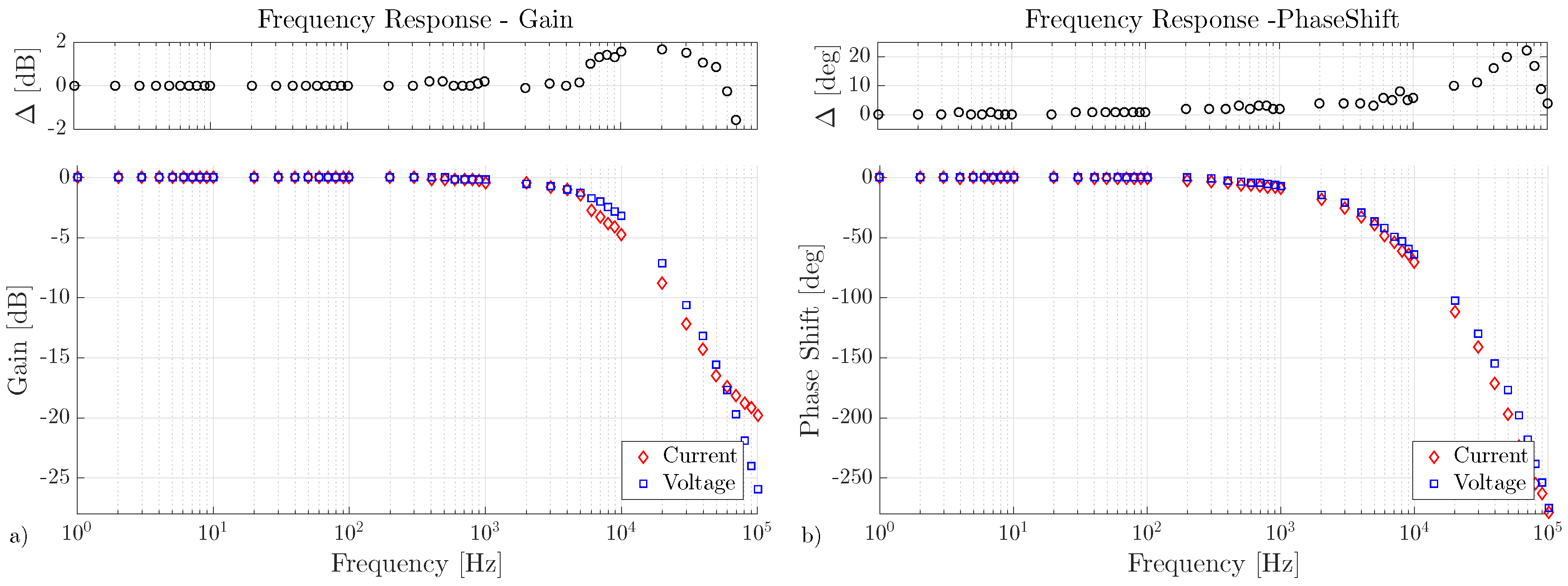
3.1.2. Frequency Response
Figure 6 shows the frequency response for both voltage and current measurements. The upper supplementary plots show the difference, in gain or phase shift, between the voltage and current measurements. It can be seen that, within 0–1 kHz, there are no significant differences. The voltage PCB shows a cut-off frequency of 10 kHz, and a damping of
dB at 1 kHz. The current PCB shows a cut-off frequency of 7 kHz, and a damping of
dB at 1 kHz. The deviation seen in the current gain, above 50 kHz, can be explained by the current sensor bandwidth.
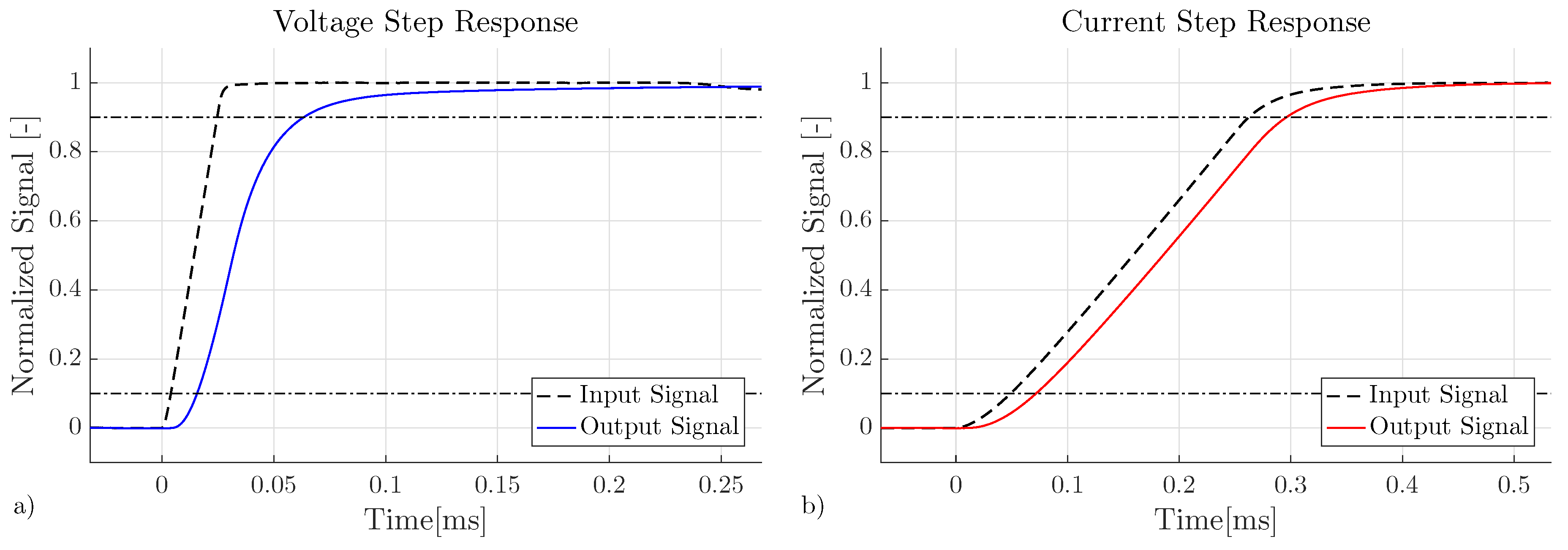
3.1.3. Step Response
Figure 7 shows step responses for voltage and current measurements. Applying a 250 mV input step to the voltage PCB, with input rise time of
= 21
s, resulted in an output step response time
= 48
s and a response time, up to 10%, of 16
s, seen in
Figure 7a. Applying a 120 A input step to the current PCB, with input rise time
= 214
s, resulted in an output step response time of
= 225
s and a response time, up to 10%, of 72
s, seen in
Figure 7b. Note that the input step is significantly slower for the current test, compared to the voltage test, due to the inductance from winding the input signal wire through current sensor, as described in the method section. The measured step response is therefore significantly slower than it would be for an ideal input step.
3.1.4. Power Consumption
With a 24 V feed, the voltage PCB consumed 20.8 mA and the current PCB consumed 22.8 mA during standby. As expected, they showed no significant change in consumption with varying AC input signal.
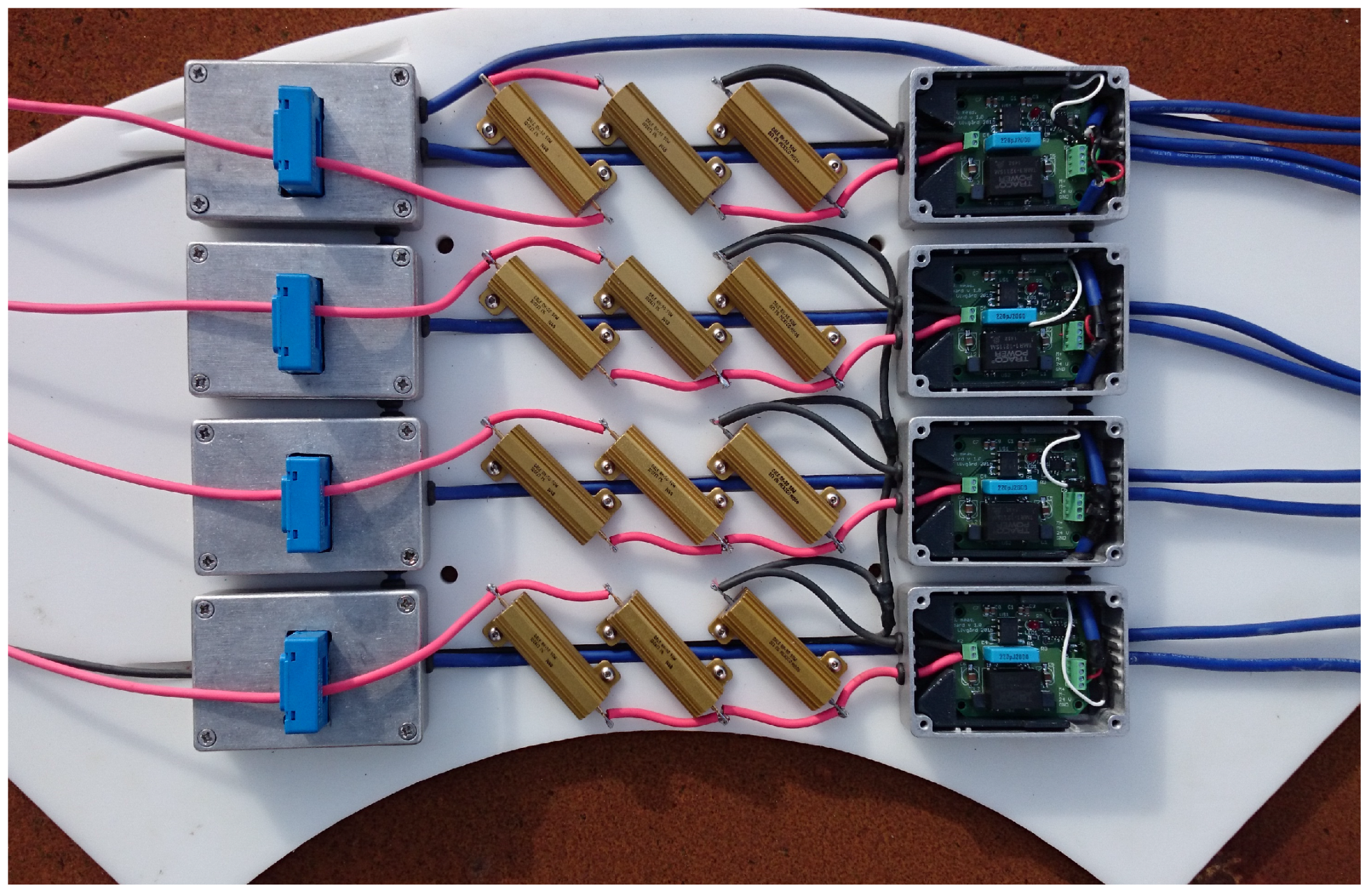
3.2. The Full Measurement System
Figure 8 shows the generator measurement board, with current measurements (boxes to the left) and voltage measurements (boxes to the right), for both AC and DC measurements, as described in
Figure 3. It also shows the power resistors used to scale down the generator voltage before entering the voltage measurement system.
The full measurement range of the system is ± 1560 V and ± 420 A on the AC side, and ±3125 V and ±560 A on the DC side. With a measured cut-off frequency of 10 kHz and 7 kHz, and a step response of 48 s and 214 s, both voltage and current measurement will be able to operate the full measurement range of 1 kHz with good signal representation.
Given a measured current consumption of 20.8 mA for the voltage PCB and 22.8 mA for the current PCB, they consume around 0.5 W each, at 24 V feeding. The expected power consumption for all AC measurements is 3.1 W, including three voltage measurements and three current measurements. It is not expected to vary with signal input. The two DC measurements and the position measurement will only operate in the positive measurement range, utilizing the 4–12 mA range. The power consumption for these measurement units will be 1.0–1.5 W, with a variation depending on the input signal.
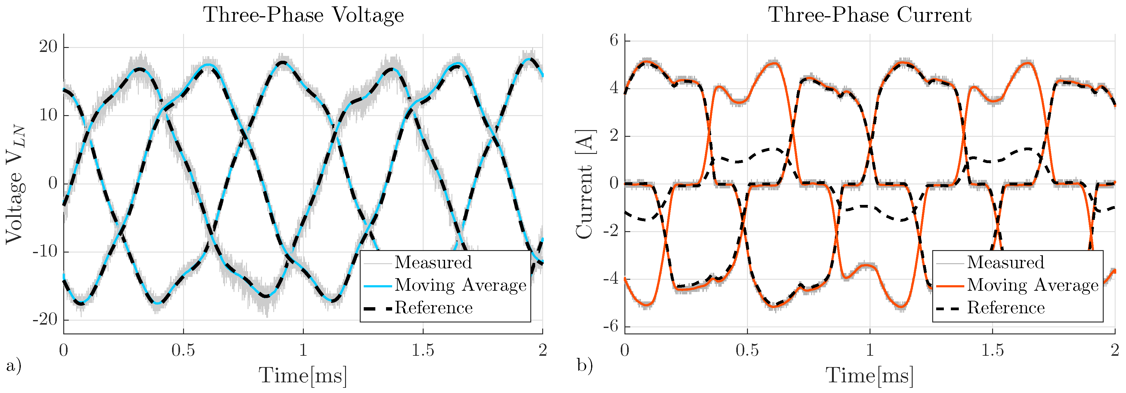
3.3. Generator Tests—Results and Evaluation
Figure 9 shows three-phase AC measurements of voltage and current from the generator during onshore tests. The unfiltered lines show the measurement system raw data, while the dotted lines are (automatically filtered) reference measurements made with a PC oscilloscope. The full lines show a moving average of the measurement system data, corresponding to the filtering made by the PC oscilloscope. One of the current reference measurements is corrupt, failing in both scale and shape, as can be seen in
Figure 9b. This is due to a fault in one of the current probes used.
Table 2 presents the SNR values for each phase measurement presented in
Figure 9. Note that the measured signals are approximately 1% of the full signal range. The corresponding SNR values for the isolated PCBs, with full input signal at 1 Hz, resulted in SNR values of 58.1 for the current PCB and 58.9 for the voltage PCB.
4. Discussion
4.1. Regarding Experimental Setup
There were a few limitations in the experimental setup, which should be noted and discussed. Firstly, it was difficult to provide high current signals. The lack of a sufficiently strong signal generator made it impossible to test high amplitudes with variable frequency. A method of winding the current carrying conductor multiple turns through the current sensor was adopted, which made it possible to amplify the signal up to 21 times. The drawbacks were a limitation in step size and that it introduced an inductance in the input signal, making it hard to produce both a strong and fast input step. This resulted in a slow input step, and thus a slow measured step response for the current PCB.
The generator tests, performed with a three-phase measurement system installed in a linear generator, were limited by the generator drive options, resulting in low speed, and therefore low voltages and currents. Therefore, the calculated SNR values are not what they would be at rated speed.
4.2. Regarding Frequency Response
It is important to avoid, or at least know how to compensate for, any change in gain or phase shift created by the measurement system used. The WEC generator has a varying reactance, depending on translator speed and position as well as the connected load. Thus, a varying phase shift between the voltage and current produced in the generator is expected during operation. This phase shift is important to measure correctly when monitoring power production and when evaluating the generator performance.
The PCB frequency response, seen in
Figure 7, shows no unexpected damping within the designed bandwidth. At 1 kHz, the damping was measured to
dB for the voltage measurement and
dB for the current measurements, which corresponds to 2% and 4%, respectively. This was also seen in the linearity test (see
Figure 5a) which showed a deviating linearity constant for the 1 kHz measurement. The same is to be expected for the current PCB, with a
dB damping at 1 kHz. Due to limited current supply, this could not be tested though.
The voltage and current PCB show a significant phase above 300 Hz, following similar phase shift paths. It is the difference in phase shift, between the voltage PCB and the current PCB, that is important. As long as they show the same phase shift, it will not affect the power calculations. As seen in
Figure 6b, the difference is only around a few degrees within the 0–1 kHz range. Discrepancies above 1 kHz are not of concern since they are not within the measurement range.
4.3. Regarding Power Consumption
Improvements could be done to reduce the power consumption even further. Using shared DC/DC converters on one PCB, instead of having one per measurement, could be an option, although it compromises the modular design. Lowering the supply voltage would reduce the power consumption further, especially if a DC/DC converter with lower output voltage rating could be used.
By not using a current signal carrier, the consumption could be significantly reduced. Even so, the chosen system is still preferred because of its many advantages, and in order to remain compatible with already existing equipment for power supply and data acquisition.
5. Conclusions
A measurement system for wave power generators has been proposed and tested. PCBs for voltage and current measurements are presented together with both individual tests and tests in a three-phase wave power generator assembly.
The work presented is an important step in establishing a cheap and reliable measurement and data acquisition system for offshore monitoring of WECs. This will also require systems for buoy measurements, data synchronization, power supply and data acquisition and transfer, which have been mentioned but are not focused on in this paper. Instead, a thorough description of design and testing of the generator measurement system has been presented.
To ensure good signal readings and dynamic behavior, the PCBs were tested for linearity, gain frequency response, phase shift frequency response and step response, which all showed good results. In addition, the power consumption was measured with results as expected. Although not tested in offshore operation, the measurement system is proven accurate, fast and easy to install. It can be used for both AC and DC power measurements, or to facilitate external transducers, such as the draw wire sensor. Furthermore, input ranges can easily be changed, by choosing another input rating for the current transducer, or by changing the external power resistors to the voltage measurements. This makes the measurement system flexible to use with different generator models.
For future work, improvements can be made to reduce the power consumption further. By gathering multiple measurements on the same PCB, both power consumption, due to a reduced number of DC/DC-converters, and manufacturing costs can be reduced. Lowering the supply voltage is also an option. To further reduce the number of signal cables, multiplexing could be used to accommodate multiple measurements on the same signal. In these cases, full sampling frequency is not needed.
Acknowledgments
The authors would like to thank Vargöns Research Foundation for supporting this work.
Author Contributions
L.U. and T.K. conceived and designed the PCBs and performed the PCB tests; L.U. planned and performed the generator experiments; M.L. provided the experiment facilities; L.U. and T.K. analyzed the data; and L.U. wrote the paper.
Conflicts of Interest
The authors declare no conflict of interest. The founding sponsors had no role in the design of the study; in the collection, analyses, or interpretation of data; in the writing of the manuscript, or in the decision to publish the results.
Abbreviations
The following abbreviations are used in this manuscript:
| WEC | Wave Energy Converter |
| PCB | Printed Circuit Board |
| AC | Alternating Current |
| DC | Direct Current |
| SNR | Signal-to-Noise Ratio |
References
- Holmes, B.; Nielsen, K. Guidelines for the Development & Testing of Wave Energy Systems; NHMRC: Canberra, Australia, 2010. [Google Scholar]
- Martinez Luengo, M.; Kolios, A.; Wang, L. Structural Health Monitoring of Offshore Wind Turbines: A review through the Statistical Pattern Recognition Paradigm. Renew. Sustain. Energy Rev. 2016, 64, 91–105. [Google Scholar] [CrossRef]
- Astariz, S.; Iglesias, G. Wave Energy vs. Other Energy Sources: A Reassessment of the Economics. Int. J. Green Energy 2016, 13. [Google Scholar] [CrossRef]
- Lu, B.; Li, Y.; Wu, X.; Yang, Z. A review of recent advances in wind turbine condition monitoring and fault diagnosis. In Proceedings of the 2009 IEEE Power Electronics and Machines in Wind Applications, Lincoln, NE, UEA, 24–26 June 2009; pp. 1–7.
- Leijon, M.; Boström, C.; Danielsson, O.; Gustafsson, S.; Haikonen, K.; Langhamer, O.; Strömstedt, E.; Stålberg, M.; Sundberg, J.; Svensson, O.; et al. Wave energy from the north sea: Experiences from the lysekil research site. Surveys Geophys. 2008, 29, 221–240. [Google Scholar] [CrossRef]
- Parwal, A.; Remouit, F.; Hong, Y.; Francisco, F.; Castellucci, V.; Hai, L.; Ulvgård, L.; Li, W.; Lejerskog, E.; Baudoin, A. Wave Energy Research at Uppsala University and The Lysekil Research Site, Sweden: A Status Update. In Proceedings of the 11th European Wave and Tidal Energy Conference, Nantes, France, 6–11 September 2015; pp. 1–10.
- Boström, C.; Svensson, O.; Rahm, M.; Lejerskog, E.; Savin, A.; Strömstedt, E.; Engström, J.; Gravråkmo, H.; Haikonen, K.; Waters, R.; et al. Design proposal of electrical system for linear generator wave power plants. In Proceedings of the IEEE IECON Industrial Electronics Conference, Porto, Portugal, 3–5 November 2009; pp. 4393–4398.
- Svensson, O.; Strömstedt, E.; Savin, A.; Leijon, M. Sensors and Measurements Inside the Second and Third Wave Energy Converter at the Lysekil Research Site. In Proceedings of the 2011 EWTEC, Southampton, UK, 5–9 September 2011.
- Tyrberg, S.; Svensson, O.; Kurupath, V.; Engström, J.; Strömstedt, E.; Leijon, M. Wave buoy and translator motions-on-site measurements and simulations. IEEE J. Ocean. Eng. 2011, 36, 377–385. [Google Scholar] [CrossRef]
- Boström, C.; Rahm, M.; Svensson, O.; Strömstedt, E.; Savin, A.; Waters, R.; Leijon, M. Temperature Measurements in a Linear Generator and Marine Substation for Wave Power. J. Offshore Mech. Arct. Eng. 2012, 134, 021901. [Google Scholar] [CrossRef]
- Lindblad, L.; Baudoin, A.; Leijon, M. Measurement System for Wave Energy Converter: Design and Implementation. In Proceedings of the Volume 9A: Ocean Renewable Energy, San Francisco, CA, USA, 8–13 June 2014.
- Amirat, Y.; Benbouzid, M.E.H.; Al-Ahmar, E.; Bensaker, B.; Turri, S. A brief status on condition monitoring and fault diagnosis in wind energy conversion systems. Renew. Sustain. Energy Rev. 2009, 13, 2629–2636. [Google Scholar] [CrossRef]
- Legowski, S.F.; Sadrul Ula, A.H.M.; Trzynadlowski, A.M. Instantaneous power as a medium for the signature analysis of induction motors. IEEE Trans. Ind. Appl. 1996, 32, 904–909. [Google Scholar] [CrossRef]
- Wenxian, Y.; Tavner, P.J.; Crabtree, C.J.; Wilkinson, M. Cost-Effective Condition Monitoring for Wind Turbines. IEEE Trans. Ind. Electron. 2010, 57, 263–271. [Google Scholar] [CrossRef]
- Ekström, R.; Baudoine, A.; Rahm, M.; Leijon, M. Marine substation design for grid-connection of a research wave power plant on the Swedish West coast. In Proceedings of the 2013 EWTEC, Aalborg, Denmark, 2–5 September 2013.
- Ekström, R.; Kurupath, V.; Svensson, O.; Leijon, M. Measurement system design and implementation for grid-connected marine substation. Renew. Energy 2013, 55, 338–346. [Google Scholar] [CrossRef]
- Monmasson, E.; Cirstea, M. FPGA Design Methodology for Industrial Control Systems—A Review. IEEE Trans. Ind. Electron. 2007, 54, 1824–1842. [Google Scholar] [CrossRef]
- Texas Instruments. 4–20 mA Current Loop Transmitters. In XTR115 Data Sheet; Texas Instruments Incorporated: Dallas, TX, USA, January 2000; [Revised November 2003]. [Google Scholar]
- LEM. Current Transducer HAIS 50..400-P. In HAIS150-P and HAIS200-P Data Sheet; LEM: Geneva, Switzerland, November 2014. [Google Scholar]
- Cristaldi, L.; Ferrero, A.; Lazzaroni, M.; Ottoboni, R. A linearization method for commercial Hall-effect current transducers. IEEE Trans. Instrum. Meas. 2001, 50, 1149–1153. [Google Scholar] [CrossRef]
- Texas Instruments. Fully-Differential Isolation Amplifier. In AMC1200/B Data Sheet; Texas Instruments Incorporated: Dallas, TX, USA, April 2011; [Revised July 2015]. [Google Scholar]
- Micro-Epsilon. Instruction Manual wire sensor WDS. In WDS-5000-P115-PA-C Datasheet; Micro-Epsilon: Uhingen, Germany, May 2015. [Google Scholar]
- Traco Power. DC/DC Converters. In TMR1-2411SM Data Sheet; Traco Power: Baar, Switzerland, August 2013. [Google Scholar]
- Avago Technologies. Double Heterojunction AlGaAs Red LED Lamps. In HLMP-K150 Data Sheet; AvagoTechnologies: San Jose, CA, USA, March 2013. [Google Scholar]
- Texas Instruments. High Voltage, High Current Operation Amplifier. In OPA549 Data Sheet; Texas Instruments Incorporated: Dallas, TX, USA, March 1997; [Revised October 2005]. [Google Scholar]
- Vishay. Wirewound Resistors, Industrial Power, Aluminum Housed, Chassis Mount. In Vishay-RH050 Data Sheet; Vishay: Malvern, PA, USA, June 2016. [Google Scholar]
Figure 1.
Schematic of the offshore wave power site and the linear generator design. The water depth at site is 25 m and the cable distance between site and onshore measurement station is around 3 km. The red rings mark places where measurements are needed.
Figure 1.
Schematic of the offshore wave power site and the linear generator design. The water depth at site is 25 m and the cable distance between site and onshore measurement station is around 3 km. The red rings mark places where measurements are needed.
Figure 2.
Circuit layout for voltage measurements (a) and current measurements (b). Circuitry and components placed outside the dotted lines are external to the PCB. Striped areas represent galvanic isolation. Some ancillary components have been left out to improve readability.
Figure 2.
Circuit layout for voltage measurements (a) and current measurements (b). Circuitry and components placed outside the dotted lines are external to the PCB. Striped areas represent galvanic isolation. Some ancillary components have been left out to improve readability.
Figure 3.
Schematic of measurement system installtion inside the WEC. Equipment placed on the measurement board is marked out with dotted lines. The DC side of the measurement board is only used if the generator is equipped with an AC/DC converter. represent the 4–20 mA signal cables.
Figure 3.
Schematic of measurement system installtion inside the WEC. Equipment placed on the measurement board is marked out with dotted lines. The DC side of the measurement board is only used if the generator is equipped with an AC/DC converter. represent the 4–20 mA signal cables.
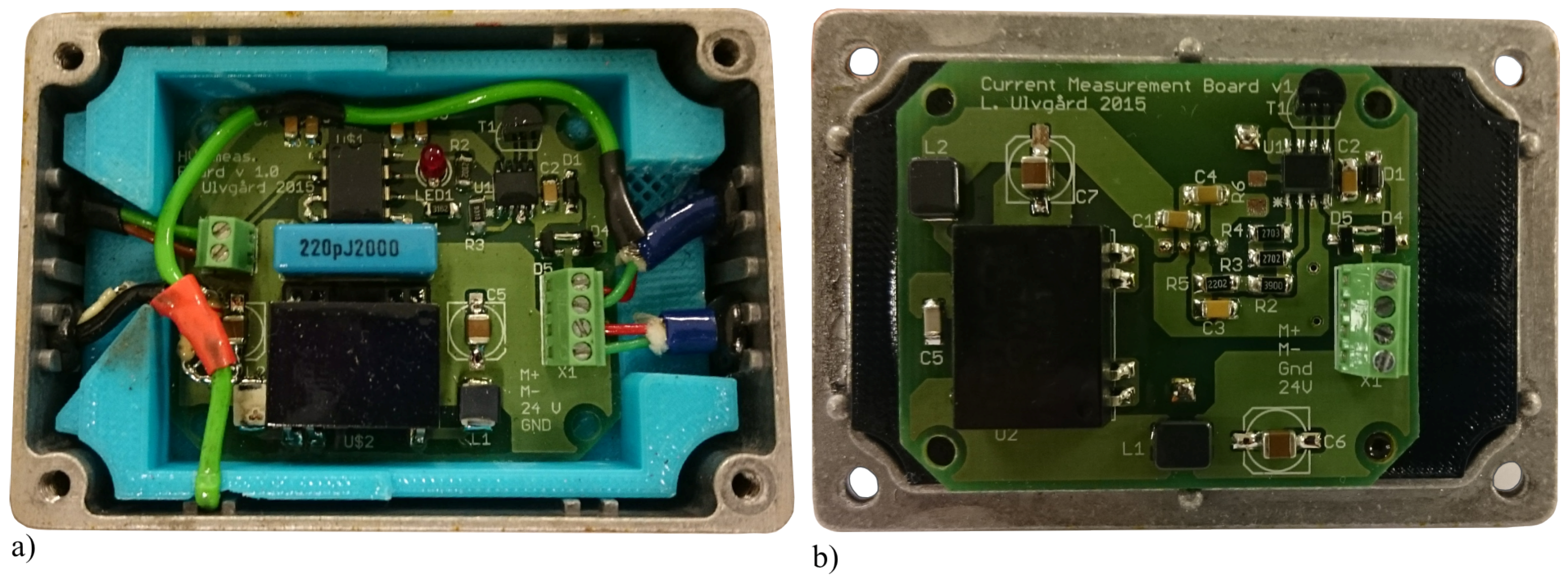
Figure 4.
Picture of the voltage PCB (a) and the current PCB (b), installed in protective shielding boxes.
Figure 4.
Picture of the voltage PCB (a) and the current PCB (b), installed in protective shielding boxes.
Figure 5.
Linearity test results for (a) voltage measurements, performed at 10 Hz, 100 Hz and 1 kHz, and for (b) current measurements, performed at 50 Hz.
Figure 5.
Linearity test results for (a) voltage measurements, performed at 10 Hz, 100 Hz and 1 kHz, and for (b) current measurements, performed at 50 Hz.
Figure 6.
(a) frequency gain response and (b) frequency phase shift response, for both voltage measurements (blue squares) and current measurements (red diamonds). Upper plots show differences in gain or phase shift between the voltage and current measurements.
Figure 6.
(a) frequency gain response and (b) frequency phase shift response, for both voltage measurements (blue squares) and current measurements (red diamonds). Upper plots show differences in gain or phase shift between the voltage and current measurements.
Figure 7.
Step response for (a) voltage PCB and (b) current PCB. Both input and output signals are normalized, and the horizontal dotted lines mark out 10% and 90%, between which the step response time is measured.
Figure 7.
Step response for (a) voltage PCB and (b) current PCB. Both input and output signals are normalized, and the horizontal dotted lines mark out 10% and 90%, between which the step response time is measured.
Figure 8.
Measurement board to be installed in the wave power generator for AC and DC measurements of voltage and current.
Figure 8.
Measurement board to be installed in the wave power generator for AC and DC measurements of voltage and current.
Figure 9.
Three-phase measurements of (a) generator voltage and (b) generator current, when connected to a resistive load via a passive rectification unit, showing the sampled (grey line) and filtered (blue or red line) measurements together with a PC oscilloscope reference measurement (dotted line). The deviant reference signal (dotted line in (b)) was due to a corrupt current probe.
Table 1.
Equipment and components used for tests of printed circuit boards.
Table 1.
Equipment and components used for tests of printed circuit boards.
| Equipment | Name | Used in Test |
| Oscilloscope for output signal reading | Tektronix TBS 1022 | 1–4 |
| Signal Generator for input voltage supply | GwInstek GPS-3303 | 1, 3, 4 |
| Transformer for current supply | Terco MV1915 | 2 |
| PC oscilloscope for step response logging | PicoScope 4424 | 5, 6 |
| Multimeter for power consumption measurements | Temna72-9280 | 7 |
| Components | Precision/Measure | Used in Test |
| 500 Ω output shunt resistor | 0.1%/- | 1–7 |
| 22 nF output filter capacitor | - | 1-7 |
| 8 Ω input shunt resistor | 1%/8.04 Ω | 1, 3, 5 |
| 1 kΩ resistors, voltage division | 0.1% | 1, 3, 5 |
| 1 Ω power resistor | 5%/1.05 Ω | 2, 4, 6 |
| , operational amplifier | - | 4 |
Table 2.
Signal-to-Noise Ratio values from generator test, with signal strengths at 1% of full measurement range.
Table 2.
Signal-to-Noise Ratio values from generator test, with signal strengths at 1% of full measurement range.
| Signal | Measured | Reference |
|---|
| Phase 1 Voltage | 27.1 | 63.3 |
| Phase 2 Voltage | 22.8 | 63.6 |
| Phase 3 Voltage | 26.6 | 62.7 |
| Phase 1 Current | 32.4 | 48.3 |
| Phase 2 Current | 31.7 | 48.5 |
| Phase 3 Current | 31.2 | 47.31 |
© 2016 by the authors; licensee MDPI, Basel, Switzerland. This article is an open access article distributed under the terms and conditions of the Creative Commons Attribution (CC-BY) license (http://creativecommons.org/licenses/by/4.0/).


