1. Introduction
The technology of organic light emitting diode (OLED) based sensors is a new and emerging field in research and development that potentially enables attractive solutions for monitoring different gas phase compositions [
1,
2], to detect dissolved molecular oxygen (O
2) species [
2] or as excitation light source for fluorescent or phosphorescent markers in biological systems and chemical processes [
2]. The OLED in photoluminescence (PL) based sensors operates commonly in pulse mode and enables by excitation the monitoring of any effects on the PL intensity induced by an analyte and also on its PL decay time. Besides PL based sensing in microscopy [
3,
4], fluorescence studies of cells [
5,
6] and forensic trace evidence [
7] are well established methods in biological and chemical studies and offer extensive possibilities to observe cell growth, metabolism behavior and toxicological effects. However, a remaining challenge is to detect changes in the PL intensity and that the excitation and emission spectrum for bio or chemical markers need to be sufficiently separated. In order to reduce the spectrally overlapping light fractions, two approaches are possible: (i) either expanding the Stokes-shift of the marker molecule as much as possible by choosing optimum emitting and excitable analytes or (ii) by applying additional optical components for the excitation source (e.g., by distributed Bragg reflectors (DBRs)) or optical filter on the photodiode (band-pass, long-pass filters). Conventional OLEDs, which are applied in combination with such optical filters, are usually based on a bottom emission architecture, where the emitted light passes through the transparent electrode and substrate [
8,
9]. In the past, optical mirrors such as DBRs have only been used to improve the light extraction for increase of the light outcoupling efficiency [
10,
11,
12,
13] or to realize optical lasing [
14]. However, there is also the possibility to integrate OLED and filter in sensor technology in very compact designs as well as nearly unlimited shapes and sizes of homogeneous emission area. Based on the emission and excitation profile, several biological and chemical processes can be detected by fluorescent or phosphorescent dye molecules. Rhodamine 6G (R6G) is a derivate of the xanthene class and a highly fluorescent dye. R6G features a high quantum yield of e.g., 95% in ethanol or water and shows an absorption peak at 530 nm in ethanol. It is often used as a water soluble tracer dye to determine the rate, transport or flow direction in bio-medical sensing applications. Moreover, the R6G dye is extensively used in biotechnology applications such as fluorescence microscopy [
3], fluorescence correlation spectroscopy [
4], flow cytometry [
8] and enzyme-linked immunosorbent assays [
15]. Optical sensors that are based on the stimulation of oxygen-sensitive dyes or derivatives of the xanthene group like R6G dyes are still in the focus of continuous effort to enhance the sensors accuracy, reliability, detection limit, operational lifetime or to reduce their cost and size [
2]. For these requirements, organic sensors can offer a wide range of advantages such as low cost production, versatility, applicability, disposability, flexibility and a compact size of the whole architecture [
2,
11], hence being very attractive for medical [
16], biological [
17,
18,
19,
20] environmental [
21,
22] and industrial applications [
17].
In this study, we investigate three OLED device architectures in top emission geometry adjusted to the needs of R6G. The OLEDs are fabricated on a 200 mm silicon wafer substrate with a variation of dielectric DBR mirrors to achieve a defined and narrow green OLED emission spectra to efficiently excite the analyte R6G for PL based sensing. The green OLEDs are combined with DBR mirror and include a thin-film encapsulation. With this architecture, it is possible to provide a sufficiently narrow OLED emission to excite R6G and to be separated from the resulting R6G emission itself. The DBR on top of the OLED is designed to stimulate the excitation maximum of R6G at 530 nm and to have a cutoff at 550 nm for minimum overlap with fluorescence of the R6G. We discuss the challenges to fabricate the DBR on top of the OLED and compare the results to a reference OLED without any mirror. Additionally, we investigate the current density—voltage characteristics (j-V), the luminance (L), the radiance (R) and external quantum efficiency (EQE) and the light emission spectra regarding loss channels and band shifts. Furthermore, the results are compared with optical simulation data taking the optical properties of DBR mirrors into account.
2. Results and Discussion
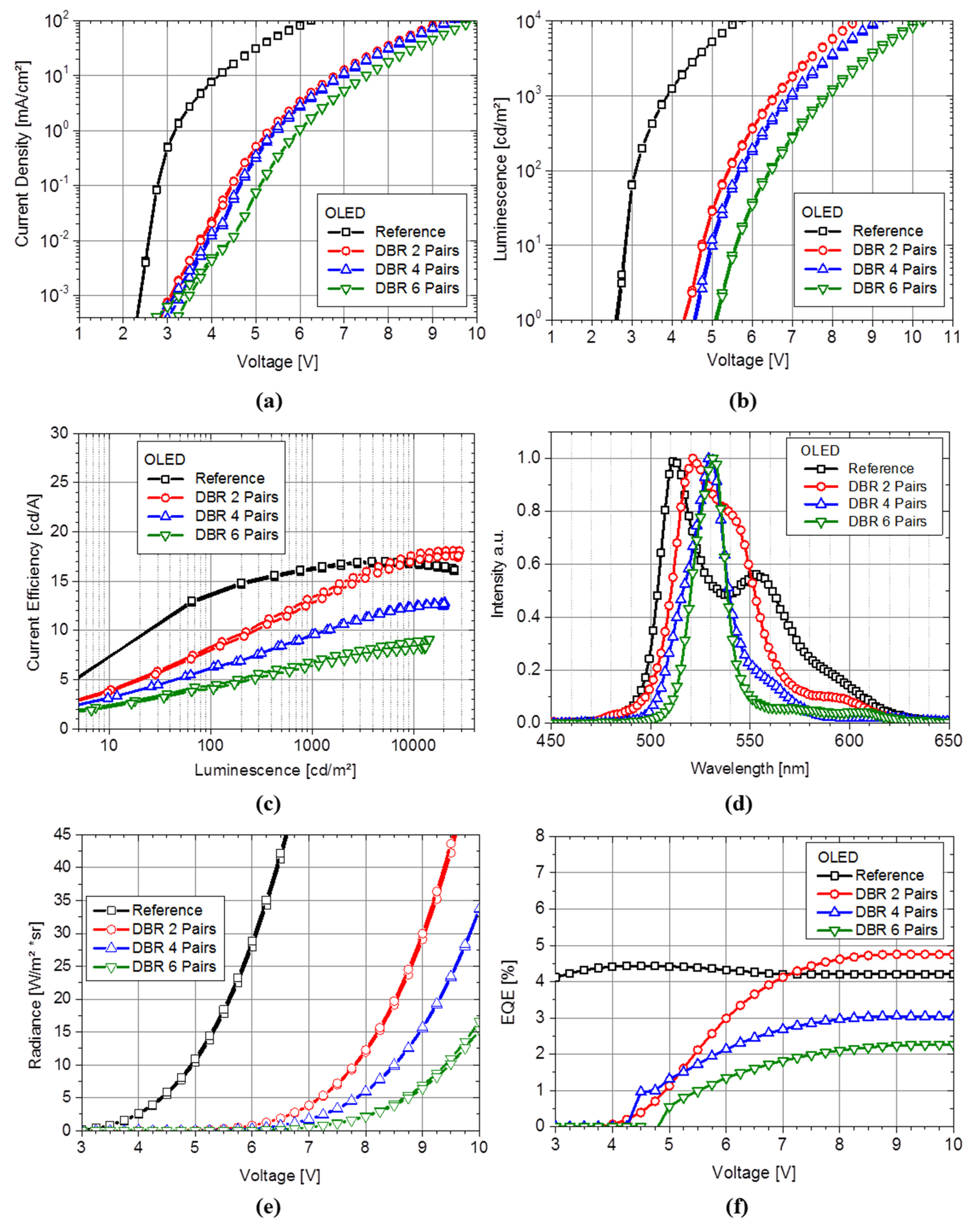
In
Figure 1, plot (a) and (b) exhibit the
J-V and
L-V characteristics, respectively. The data of the reference device (without any DBR) is represented by the black rectangles and shows a steep rise between 2 V and 3 V and a moderate increase towards 5.45 V at 50 mA/cm
2. For the reference device, the luminance (see plot b) reaches approximately 100 cd/m
2 at 3.10 V and rises up to about 8365 cd/m
2 at 5.61 V. Our reference device shows comparable results in performance to the manuscript of Peng [
23] for OLED devices with a fluorescent green top emission architecture. In comparison to the voltage V at 50 mA/cm
2, we see a fundamental shift of the operation voltage from 5.45 V for the reference to maximum of 9.08 V with increasing DBR pair number, see
Table 1. The OLED device with the highest number of DBR pairs (
n = 6 pairs, green upside-down triangle) shows the highest difference in
J-V and
L-V characteristics to the reference with no DBR-layer. The voltage at 10,000 cd/m
2 shows the same behavior and increases with the number of DBR-layers. We notice the difference between the voltage at 50 mA/cm
2 to the voltage at 10,000 cd/m
2 (see
Table 1). Further, the voltage increases in different amounts with respect to the number of applied DBR pairs. We see a large difference from 0 to two pairs and a slight difference from four to six pairs. This difference illustrates the declining efficiency in
Figure 1 with increasing number of DBR-layers. The device shows less current at a given voltage and subsequently less luminance which depends on decreased current densities for the devices with DBRs (
Figure 1a). These changes of the OLED device characteristic is caused by compressive or tensile stress [
24], which is most likely induced by the oxide DBR layers on the devices or a temperature effect [
25] to the OLED materials. A typical OLED deposition process is limited to maximum substrate temperature of 100 °C, but TiO
2 cause a temperature increase of the substrate during electronic-beam deposition of up to 120 °C, respectively. Such high deposition temperatures can cause morphology changes within the OLED layer, as well as diffusion of materials to neighboring layers and degradation of molecules. The luminous efficiency is significantly affected by the drop of the luminance at the same current density. We considered the luminance
L at 50 mA/cm
2 and compared it to simulation results. As expected, a lower efficiency at equal current density is observed. This is partly due to the losses within the device and is essential to the optical properties of the components. In comparison to the simulation of the maximum luminance relative to our measurements, we see that the simulated luminance behaves as similar as in the experiment. The OLED luminance with 0 pairs and the current density of 50 mA/cm
2 is 8365 cd/m
2 and rises as expected to 8685 cd/m
2 for the OLED with two DBR pairs. Considering the luminance of the OLED with four and six DBR pairs, we see a significant loss in the efficiency compared to the reference. Accordingly to the differences in voltage and peak efficiency we see more pronounced losses for lower luminance values between the reference OLED and the devices with DBR mirror. The current efficiency of OLEDs increase with current density up to the point of optimum recombination properties within the emitting layer [
26]. In contrast to the simulated and measured luminance we see a difference between six and four pairs of DBR. This difference is based on changed recombination properties and a variation of layer thickness in comparison to the ideal and fixed layer thickness in simulation. The results show that the addition of the DBR-layer onto the OLED device causes a shift of the maximum current efficiency towards higher current densities and luminance. As a consequence,
Figure 1c exhibits the drop of efficiency of approximately 56% at 1000 cd/m
2 for the device with maximum numbers of DBR compared to the reference device. When comparing the OLED luminance and current efficiency with the radiometric properties (
Figure 1e) and external quantum efficiency EQE (
Figure 1f), we see the same behavior. The radiance of the OLEDs decreases with increasing number of DBR pairs. In comparison to the voltage at 10 W/(m
2 × sr), we see the shift from 5.0 V (reference device) to 9.45 V (OLED device with six pairs of DBR), which resulted in the most significant shift of radiance and current density compared to the device with less DBR pairs, while a significant loss in the EQE is observed between the device with four and six DBR pairs.
Figure 1f exhibits a decreasing of EQE at 8 V from 4.2% for reference to 2.1% for device with six pair DBR. Regarding the differences in voltage and EQE we see more pronounced losses for lower radiance values between the reference OLED and the devices with DBR mirror. We attribute these changes in the electro-optical characteristics to the adoption of dielectric mirrors on top of the OLED and their thermal or mechanical influence on the organic layer during the deposition, since the OLED layer thicknesses show no changes in their SEM cross sections.
Table 1.
Comparison of measured voltage, (V at 50 mA/cm2 and V at 10 kcd/m2) and measured luminance (L at 50 mA/cm2) with the simulated luminance Lsimulated in percent normalized to reference organic light emitting diodes (OLED) depending on the distributed Bragg reflector (DBR) structure.
Table 1.
Comparison of measured voltage, (V at 50 mA/cm2 and V at 10 kcd/m2) and measured luminance (L at 50 mA/cm2) with the simulated luminance Lsimulated in percent normalized to reference organic light emitting diodes (OLED) depending on the distributed Bragg reflector (DBR) structure.
| Pairs | V at 50 mA/cm2 | V at 10,000 cd/m2 | L at 50 mA/cm2 | Lmeasured | Lsimulated | EQE at 8 V |
|---|
| N | (V) | (V) | (cd/m2) | (%) | (%) | (%) |
|---|
| 0 | 5.45 | 5.61 | 8365 | 100 | 100 | 4.2 |
| 2 | 8.43 | 8.58 | 8685 | 104 | 110 | 4.6 |
| 4 | 8.52 | 9.12 | 5980 | 71 | 79 | 3.0 |
| 6 | 9.08 | 10.12 | 4104 | 49 | 43 | 2.1 |
Figure 1.
(a) Current density to voltage curve (J-V curve) of all devices; (b) determined luminance characteristic of the devices; (c) current efficacy vs. luminance and (d) the emission spectra of the devices in variation of the mirror pair number measured perpendicular to the OLED surface. Figure (e) and (f) show the radiometric values: (e) the radiance depending on voltage and (f) the external quantum efficiency.
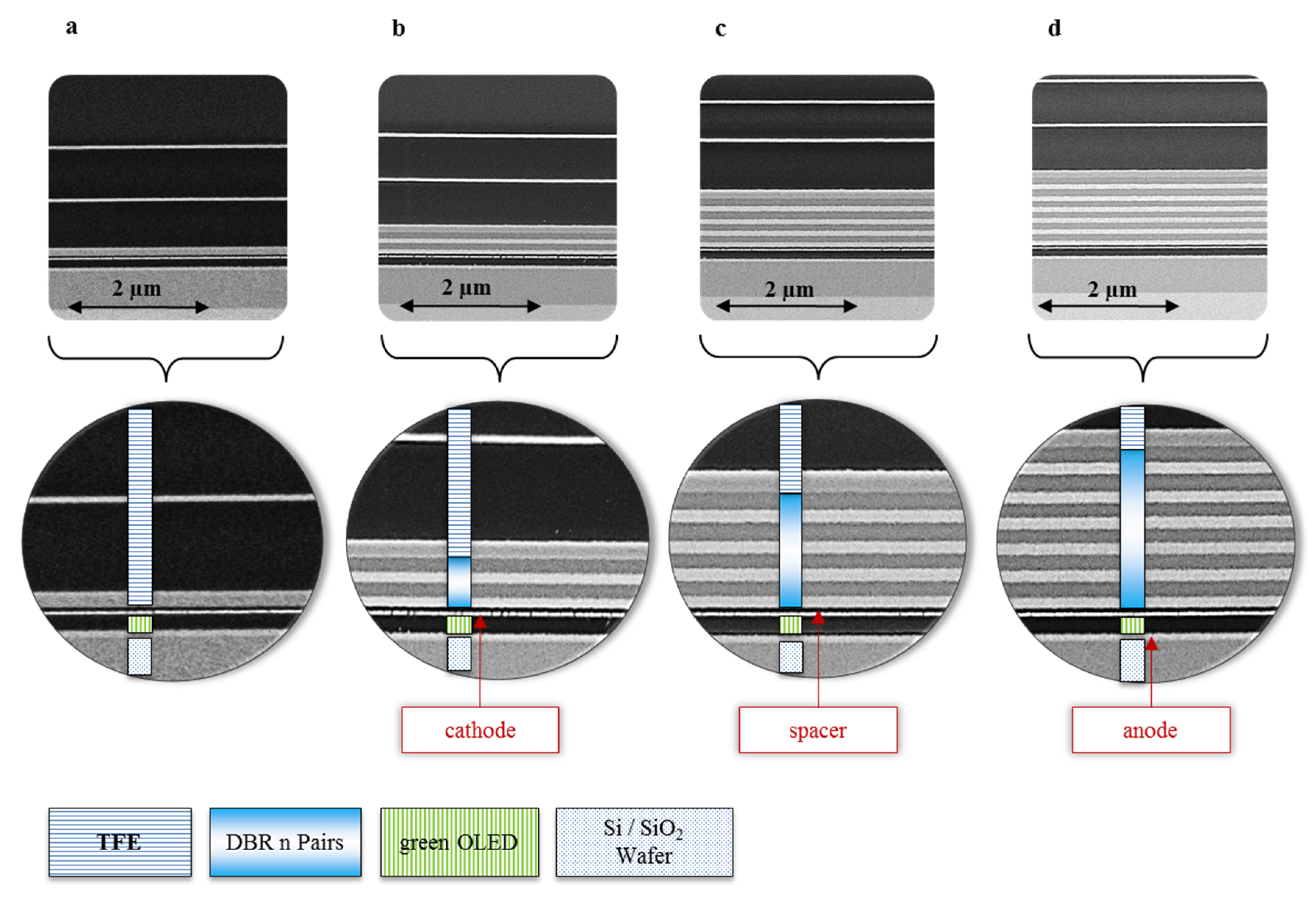
Figure 2 exhibits the cross section of the OLED devices with DBR mirrors. The sequence of the dielectric layers can be identified and does not show any interface defects between spacer layer and DBR or any delamination of organic layers from the contacts. However, looking in more detail, we notice a discontinuity of our silver cathode at each device. We believe that this is not originating from a temperature effect or induced stress during the DBR deposition; moreover, it can be assigned to the typical thin film formation behavior of silver during deposition. Similar effects are also described in the work of Lee and Schubert
et al. [
27,
28,
29].
Since the main focus of our experiment is based on organic sensor technology and the narrowing of the OLED emission spectra to stimulate the R6G, we consider the imperfections of the silver layer as negligible. The reduction to a narrow emission spectra of the OLED at 530 nm wavelength is essential and a crucial point in this study. In
Figure 1d, we present the resulting emission profile variation at a luminance of 1000 cd/m
2.
Figure 2.
Cross section of the OLED devices including the variation of DBR layer and fixed TFE-thicknesses, (a) shows the reference OLED; (b) shows two pairs of DBR on top of OLED including TFE (2.0 kV/1.6 mm × 20.0 k); (c) shows four pairs of DBR (2.0 kV/1.8 mm × 20.0 k) and (d) exhibits six pairs of DBR above the OLED and below the TFE with (2.0 kV/2.3 mm × 20.0 k).
The emission spectrum for the reference device is located between 480 nm and 630 nm with a maximum at 510 nm. The DBR mirror uses the transmission with a defined stop band and acts as dielectric mirror. With increasing numbers of DBR pairs, the emission maxima shift towards 530 nm while also reducing the full width at half maximum (FWHM). Whereas the significance of emission maximum variation reduces with every additional DBR pair (510 nm with 0 pairs, 521 nm with two pairs, 530 nm with four and six pairs), the FWHM width decreases with each new pair (42 nm with two pairs, 24 nm with four pairs, 18 nm with six pairs).
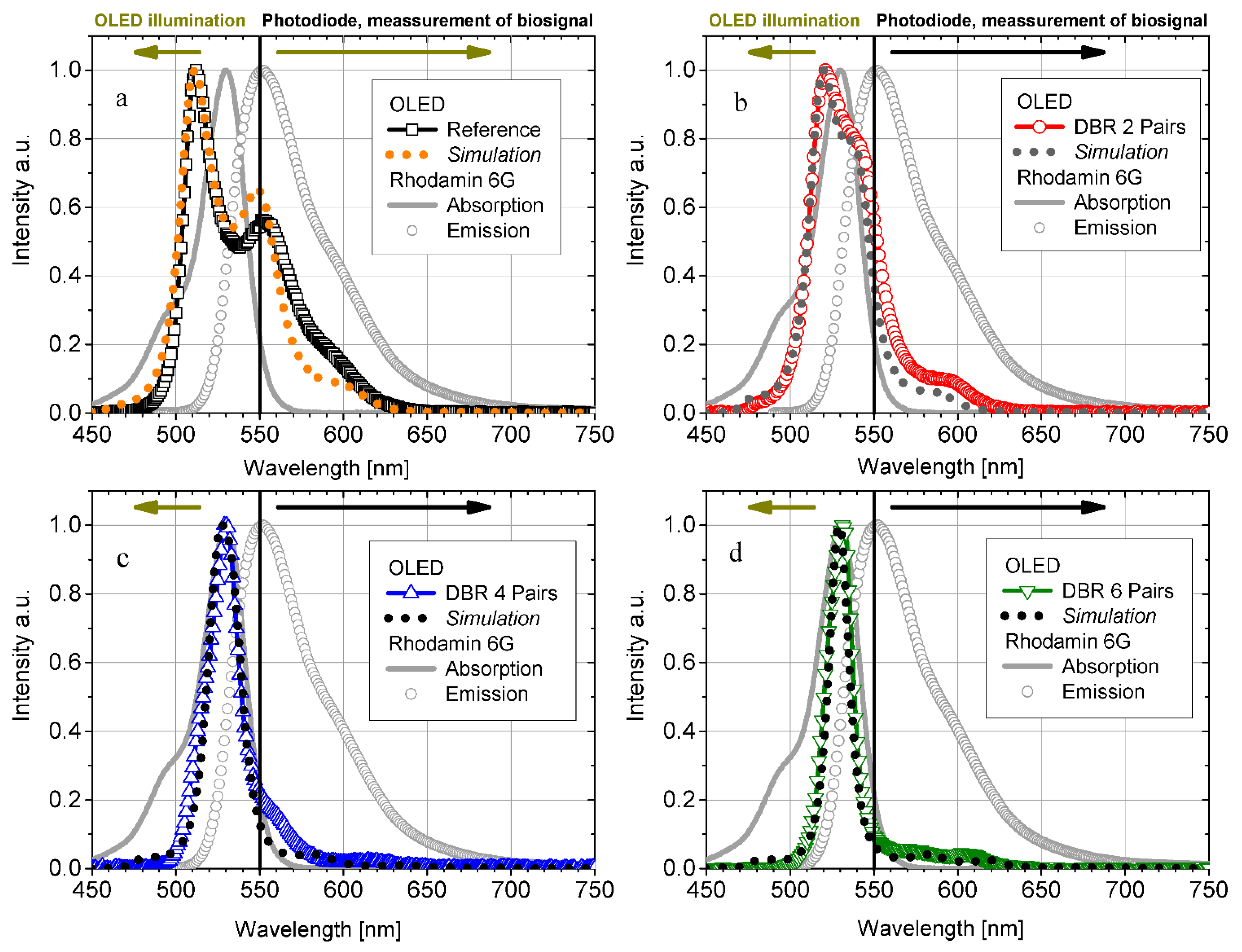
Figure 3a,b illustrate the emission spectra of individual OLEDs depending on mirror properties. To separate the excitation spectra from the emission a sharp cut off at 550 nm for R6G is needed. In
Figure 3a, the reference device without any mirror shows a significant overlap at 550 nm and a deviation in maximum of excitation. In contrast to the reference, the devices with DBR mirror exhibit a substantial improvement to stimulate the absorption of the pigment.
Figure 3.
All graphs express the normalized spectral radiance as intensity. The graphs in (a) exhibit the spectral emission of the reference OLED in comparison to the OLED devices with including DBR mirror; (b) two DBR Pairs; (c) four DBR pairs; (d) six DBR pairs. The grey solid line presents the excitation spectra and the open dotted line the emission spectra of R6G in a water solution excited and recorded with a Fluoromax-4 from Horiba Jobin Yvon. Furthermore, the figures demonstrate the result of our experiment with the previous simulation.
As depicted in
Figure 3b, we achieved a reduced overlap and a shift of the emission peak towards 530 nm for two DBR pairs. Consequently,
Figure 3c,d reveal that devices comprising four and six DBR pairs are featured by the most suitable optical properties to excite the R6G in their excitation maximum at 530 nm. The maximum of emission is located at the required peak for both devices while the six pair DBR OLED shows a good cut-off at the wavelength of 550 nm. Therefore, the OLED device with six DBR pairs demonstrates the best result to stimulate the pigment R6G and to separate the emission of the excitator and analyte. For developments in sensor technology, it is important to understand the optical properties of materials and processes as well as their impact to the final device. For comparison, the experimental data are plotted together with the results from optical simulation of the OLED emission characteristic.
Figure 3a–d illustrate the recorded, normalized spectra in comparison to the simulated emission spectra. With respect to the reference OLED, we achieved a good correlation with the simulated and recorded spectra. The simulated data and experimental results differ slightly between 530 nm and 600 nm. However, this discrepancy can be attributed to differences in the modelling of the emission characteristic of less efficient recombination centers at the green emitter molecule and is not important for the spectral shape of the design of DBR mirror.
Figure 3b–d present the experimental results and simulation data in variation of the mirror number. With increasing DBR pair number, the OLED emission characteristic is strongly modified with respect to the spectral shape as well as the FWHM, whereas the emission spectra are affected as simulated due to the increasing number of dielectric layers and the emission spectra are narrowed. This change in the emission spectrum originates from alternating thin dielectric layers of different refractive indices. Each dielectric and polymer layer boundary causes a partial reflection of an optical wave. In case the wavelength is close to four times the optical thickness of the DBR layers, the majority of reflections combine to constructive interference, and the layers act as an excellent reflector with the expected stop band at 530 nm. By comparing the measured OLED characteristics with simulation, we attribute the deviation of the optical cavity to the thickness of DBR layers, unclosed Ag cathode and a slight layer inhomogeneity in the thin film encapsulation. Optical simulations show the high sensitivity of DBR-OLED emission properties to thickness and material properties with increasing DBR thickness. Thus, the advantage of emission optimization is accompanied by an increase in requirements of multilayer deposition accuracy. Nevertheless, the variation by the number of dielectric layers as illustrated in our experiment and schematic in
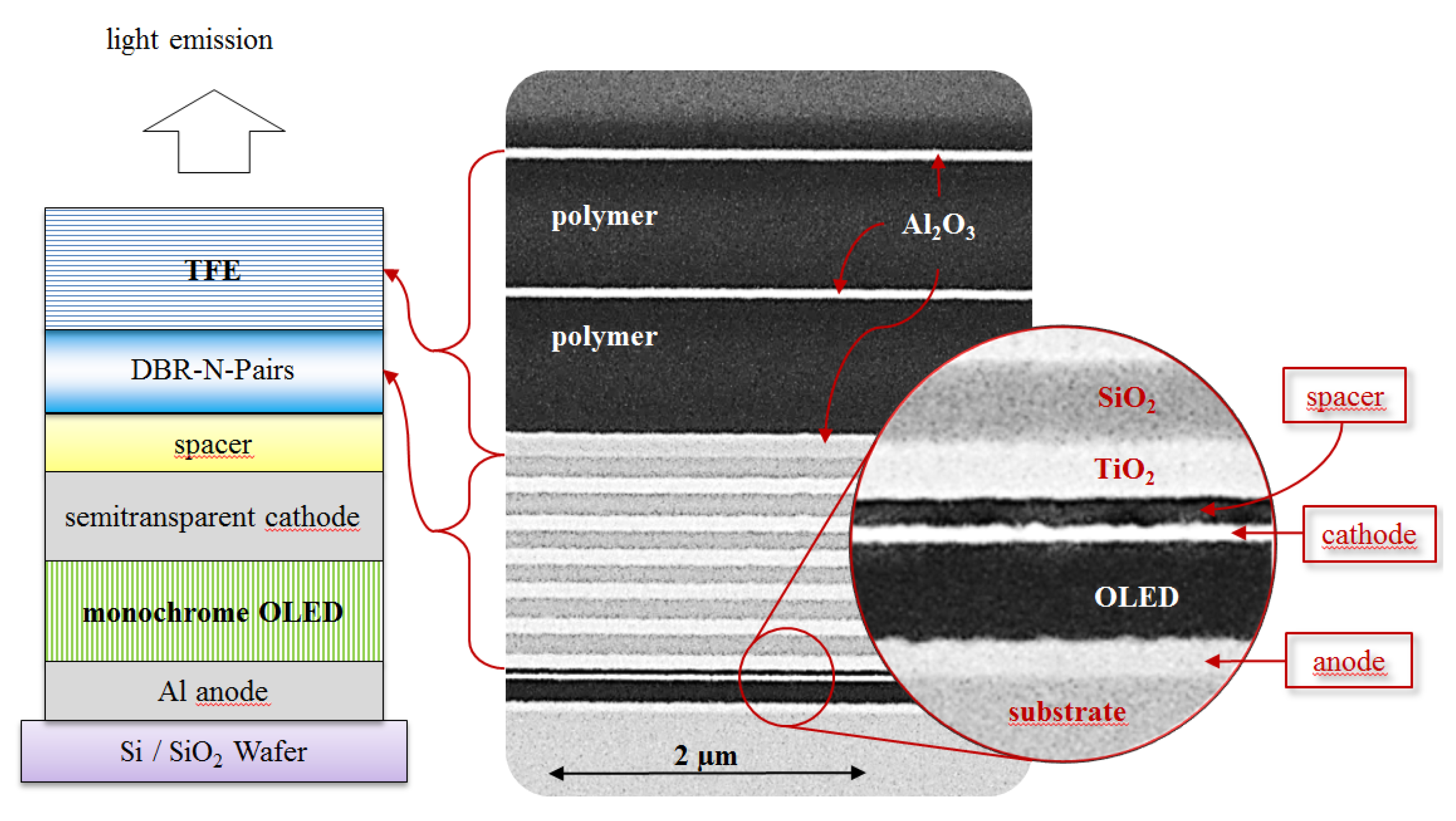
Figure 4, exhibits an alternative option to control the optical behavior of light emission for OLED devices. The possibility to modify the light emission behavior of OLEDs by using optical mirrors like DBR has been demonstrated and can be applied for sensing such as illuminating R6G.
Figure 4.
Schematic presentation of the device architecture including the top-emitting OLED, the DBR and the thin film encapsulation. N correlates to the number of DBR pairs (N = 0, 2, 4, 6).
Figure 4.
Schematic presentation of the device architecture including the top-emitting OLED, the DBR and the thin film encapsulation. N correlates to the number of DBR pairs (N = 0, 2, 4, 6).
3. Experimental Section
For OLED device preparation, an aluminum (Al) anode was deposited via sputtering onto a silicon oxide insulation layer on the silicon substrate. Subsequently, several organic layers of the monochrome OLEDs are deposited on top of the structured anode by vapor thermal evaporation (VTE) under a base pressure of 2 × 10
−7 mbar. The total OLED thickness is 108 nm and comprises different functional layers such as the hole injection layer (HIL) and a hole transport layer (HTL). The HIL consists of 1,4,5,8,9,11 -hexa-azatriphenylene hexacarbonitrile (HATCN; 10 nm) and the HTL of
N,N′-bis(naphthalene-1-yl) -
N,N′-bis(phenyl)-2,7-diamino-9,9-spirobifluorene (spiro-NPB; 50 nm). Both materials were delivered by Nichem Fine Technology Co. Ltd (NFT) (Jhubei City, Hsinchu County, Taiwan). The emission layer (20 nm) consisting of a host material and 5% dopant material and were provided from Sun Fine Chemical (Ochang-eup, Cheongwon-gun, Chungcheongbuk-do, South Korea). Furthermore an electron transport layer (ETL) (28 nm) is used. The ETL based on host material delivered by Merck KGaA (Darmstadt, Germany) and a 16.8% dopant of 8-hydroxyquinolatolithium (LiQ) provided by NFT. The OLED is completed with an electrical contact which consists of a transparent cathode (2 nm Ca, 13 nm Ag) provided by Kurt J. Lesker (Hastings, England). The cross section of cathode and anode films defines the active pixel area of 2.50 × 2.54 mm
2. The OLED is finalized by depositing an organic spacer layer (30 nm) spiro-NPB delivered by NFT to reduce the thermally induced stress of the subsequent optical mirror and its influence on the underlying cathode film. The individual lateral dimensions of each layer are defined by the used shadow masks. The optical mirror consists of alternating silicon dioxide (SiO
2) and titanium dioxide (TiO
2) layers, deposited via electronic-beam evaporation with a rate of 0.2 nm/s for SiO
2 and 0.1 nm/s for TiO
2. The SiO
2 and TiO
2 materials were purchased from Kurt J. Lesker company. The DBR features 95 nm thick SiO
2 and 64 nm thick TiO
2 layer pairs. (DBR with two pairs: 318 nm total thickness, four pairs: 636 nm total thickness and six pairs: 954 nm total thickness). Finally, a 1.3 μm thick multilayer thin-film encapsulation (TFE) is applied to protect the device against damage and degradation. This TFE consists of alternating layers of aluminum oxide (Al
2O
3) provided by Kurt J. Lesker and a cross-linked acrylic polymer from JSR Micro. The TFE is made of a 100 nm Al
2O
3 layer by electronic-beam evaporation and followed by direct current sputtering of 40 nm Al
2O
3 for two times. The polymer between the Al
2O
3 is produced by a liquid-vapor-liquid deposition and is cured with UV light. More details about this thin film encapsulation system are published elsewhere [
30]. The adhesion of water within the DBR can also cause a shift of the photonic bandgap. Therefore, the TFE is used in addition to protect the optical design of the DBR. The
Figure 4 illustrates the schematic cross section of the described device architectures, as confirmed by field emission scanning electron microscopy (FE-SEM) images, while, in
Figure 5, the optical properties of the used DBR and TFE materials are shown. In addition,
Figure 2 exhibits a detailed view on the layer structure of the OLED device. The whole process of device fabrication in combination with DBR and encapsulation has been performed in cleanroom environment of class ISO 5, while only the separation of OLED devices from each other and their characterization were done under laboratory conditions. After fabrication, the devices have been characterized by means of measuring current density-voltage (
j-V), luminance-voltage (
L-V) and the electroluminescent spectra in the range from 1 to 10 V. The OLED characterization is carried out with an Autronic Melchers System (DMS401). The preparation and analysis of the cross section in
Figure 2 and
Figure 4 has been performed by a 6 kV argon ion beam (Jeol, Cross-Section Polisher SM-09010) with a beam diameter full width at half maximum of 500 µm. The characterization of these cross sections was done with an FE-SEM (Hitachi SU8000) at an accelerating voltage of 2.0 kV and different resolutions. For two-pair DBR, we are using an operating distance of 1.6 mm with a magnification of 20000 and for four-pair DBR a distance of 1.8 mm and a magnification of 20,000 and finally for the six-pair DBR, a distance of work with 2.3 mm and the same magnification like four-pair DBR.
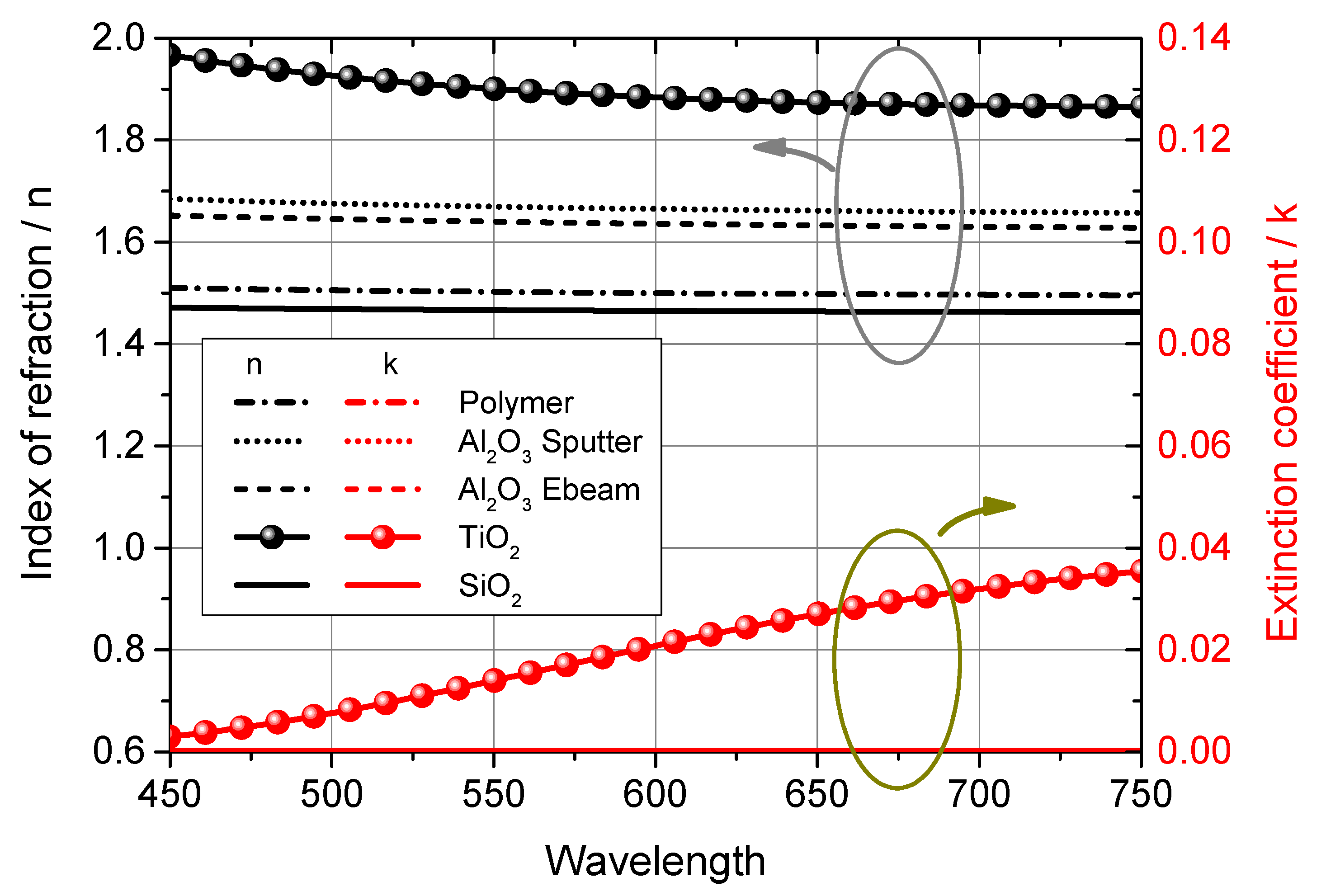
For optical simulation, we are using the emission module of the thin film optics simulation software “SETFOS”, version 3.3. SETFOS applies the transfer matrix approach to calculate the optical properties of a multilayer structure and the emission profile is derived by considering the complex refractive index and optical thickness of each layer, where
n is the refractive index and
k is the extinction coefficient and
x describe the layer thickness. We extract the optical constants such as the refractive index and extinction coefficient for organic and metal films by analyzing recorded data obtained from variable-angle spectroscopic ellipsometry (M2000 Woollam) (VASE) with an analyzer (NIR-VIS-UV VASE, J.A. Woollam Co. Inc., Lincoln, USA). The modelling principle for OLEDs is described and published elsewhere [
31,
32].
Figure 5.
The optical constants n and k for the used DBR materials and the TFE.
Figure 5.
The optical constants n and k for the used DBR materials and the TFE.


