
A Technique for Mitigating Thermal Stress and Extending Life Cycle of Power Electronic Converters Used for Wind Turbines

Abstract
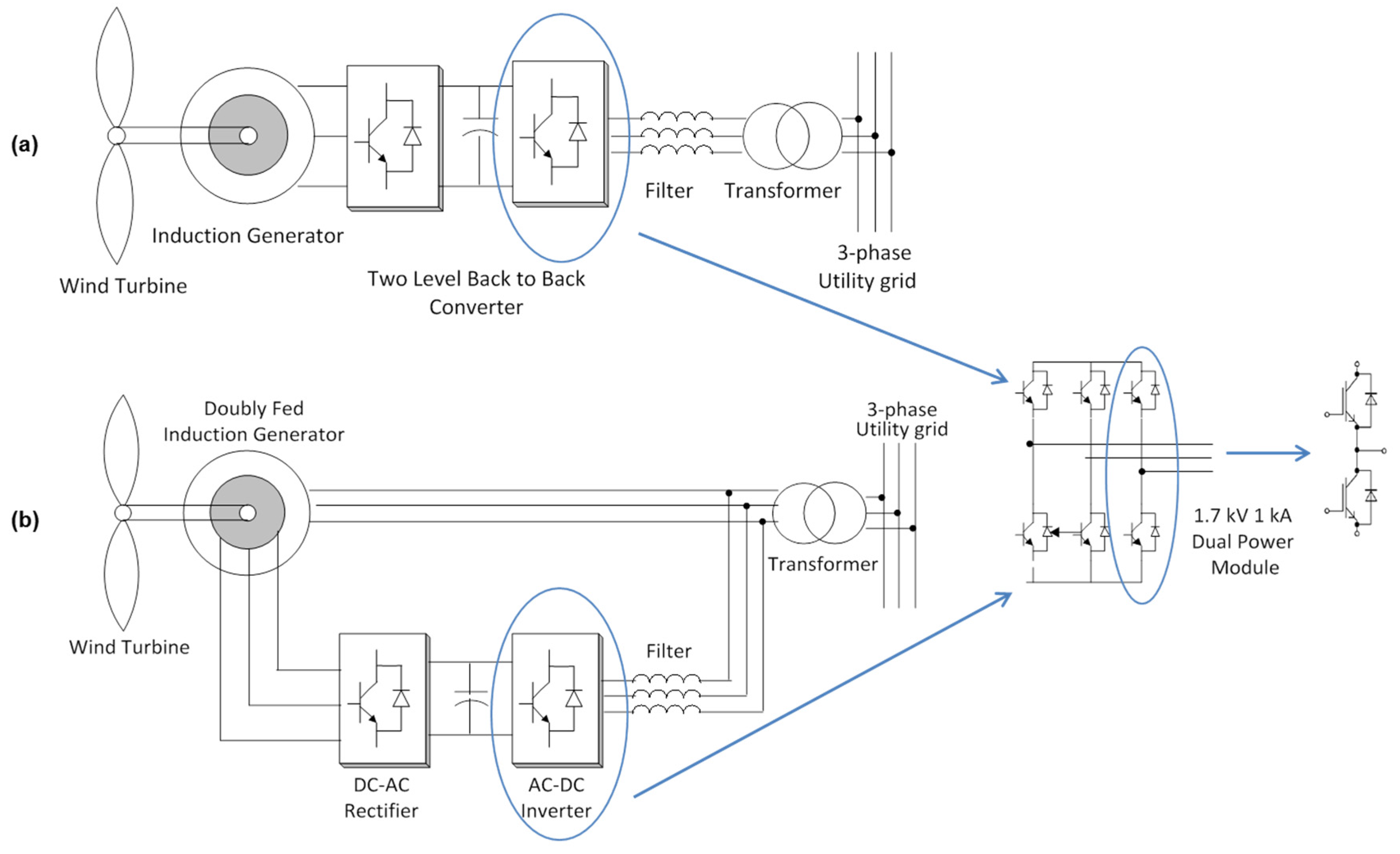
:1. Introduction
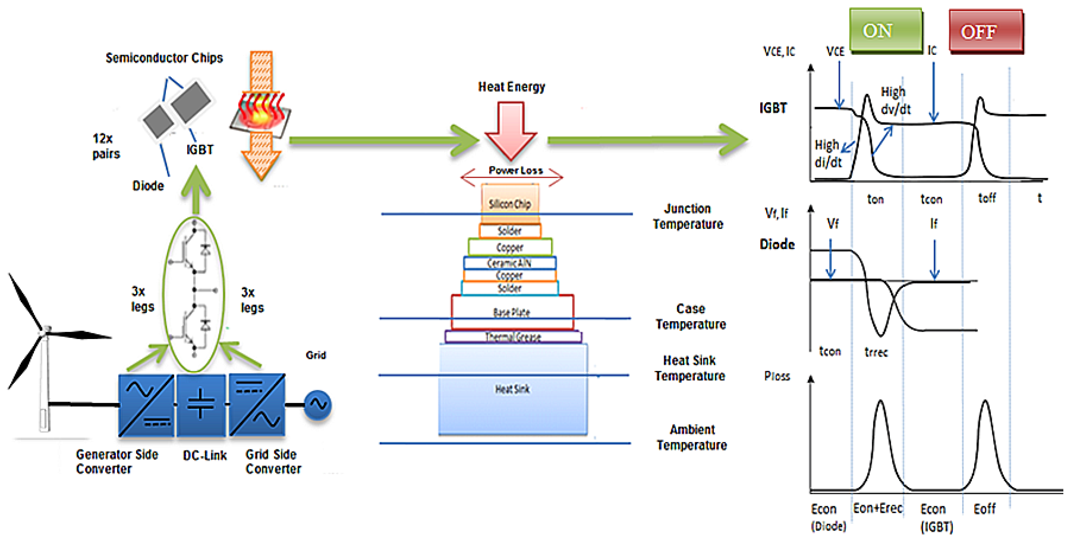
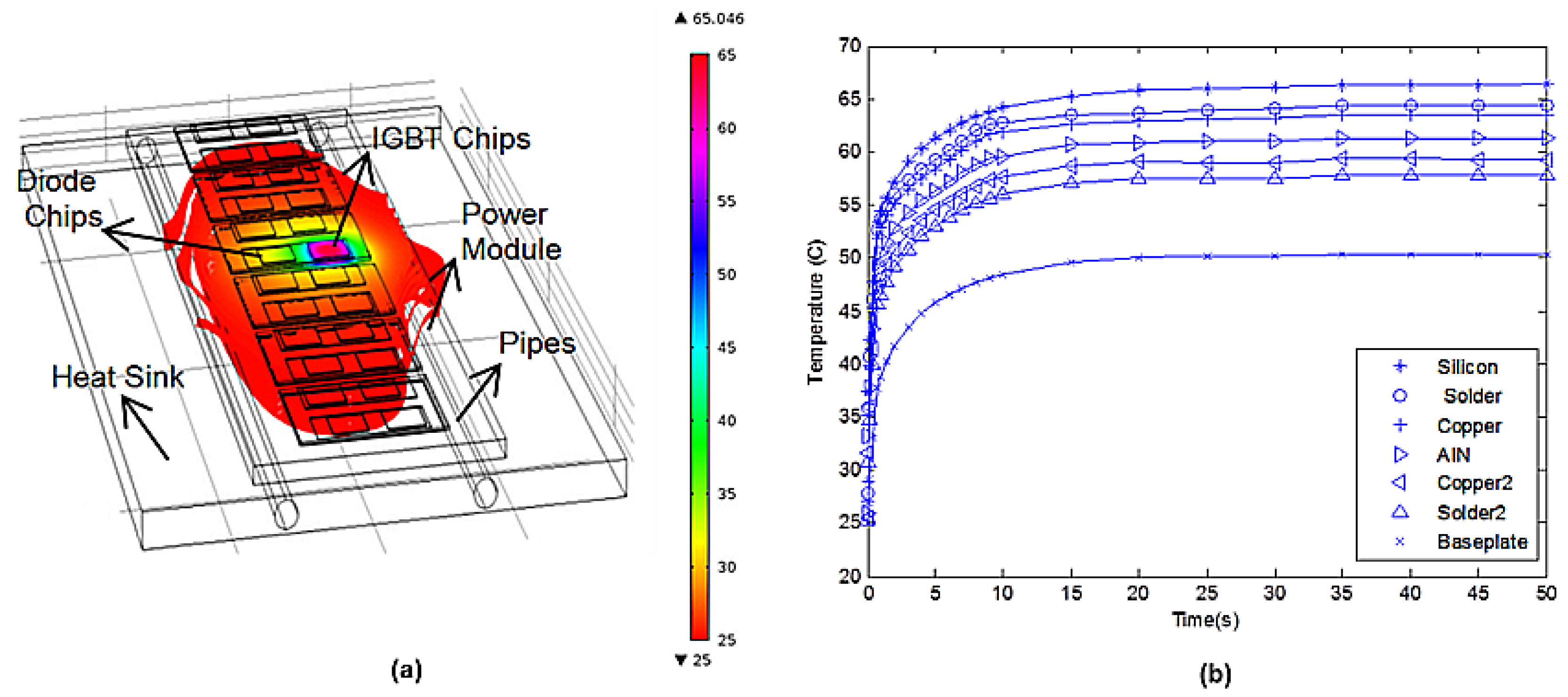
2. State of the Art Electro-Thermal Model of IGBT Power Module
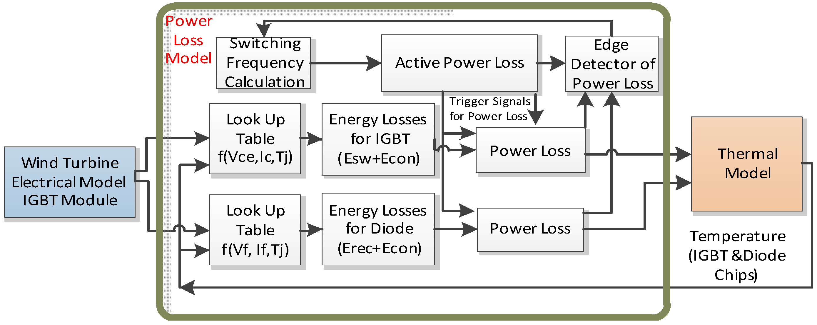
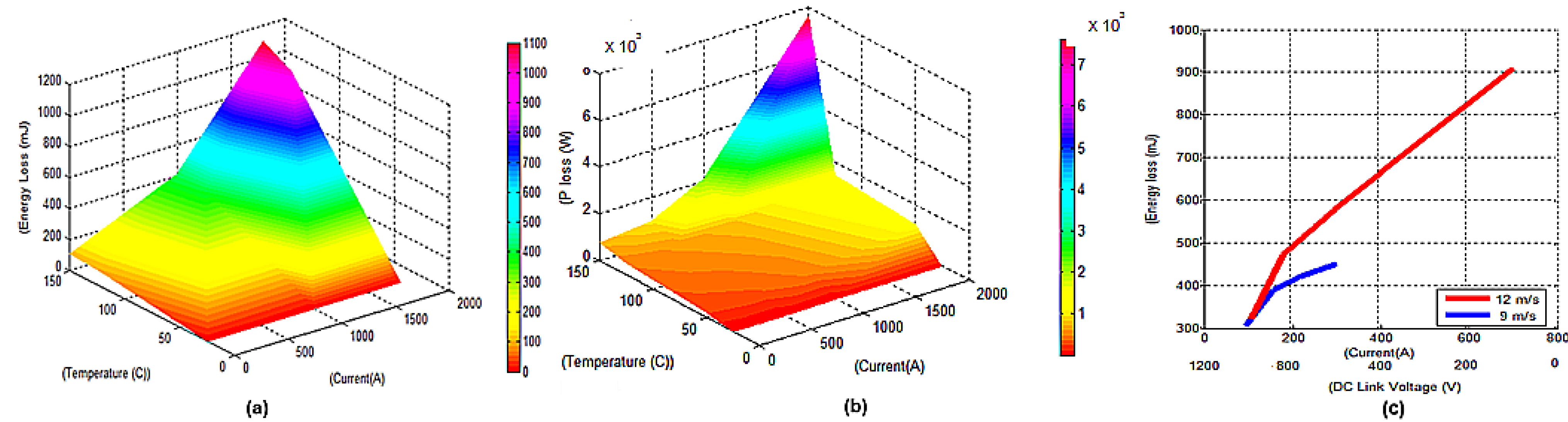
2.1. Power Loss Modelling


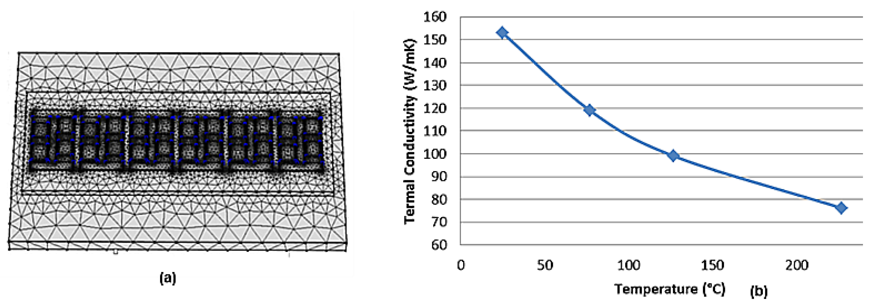
| Layer | Physical Properties at 25 °C | |||||
|---|---|---|---|---|---|---|
| ρ (kg/m3) | K (W/m·K) | c (J/(kg·K) | CTE (10−6/K) | Young Modulus (MPa) | Poisson Ratio | |
| Silicon | 2330 | 153 | 703 | 3.61 | 113.000 | 0.28 |
| Solder | 7360 | 33 | 200 | 30.20 | 27.557 | 0.40 |
| Copper | 8850 | 398 | 380 | 17.30 | 128.000 | 0.36 |
| Aluminium | 3300 | 180 | 750 | 4.60 | 344.000 | 0.22 |
| Copper | 8850 | 398 | 380 | 17.30 | 128.000 | 0.36 |
| Solder | 11,300 | 35 | 129 | 29 | 16.876 | 0.44 |
| Baseplate | 3010 | 180 | 741 | 0.27 | 192.000 | 0.24 |
| T. Grease | 2500 | 2 | 700 | 29 | 15.700 | 0.32 |
| Heat Sink | 2730 | 155 | 893 | 4.30 | 384.000 | 0.30 |
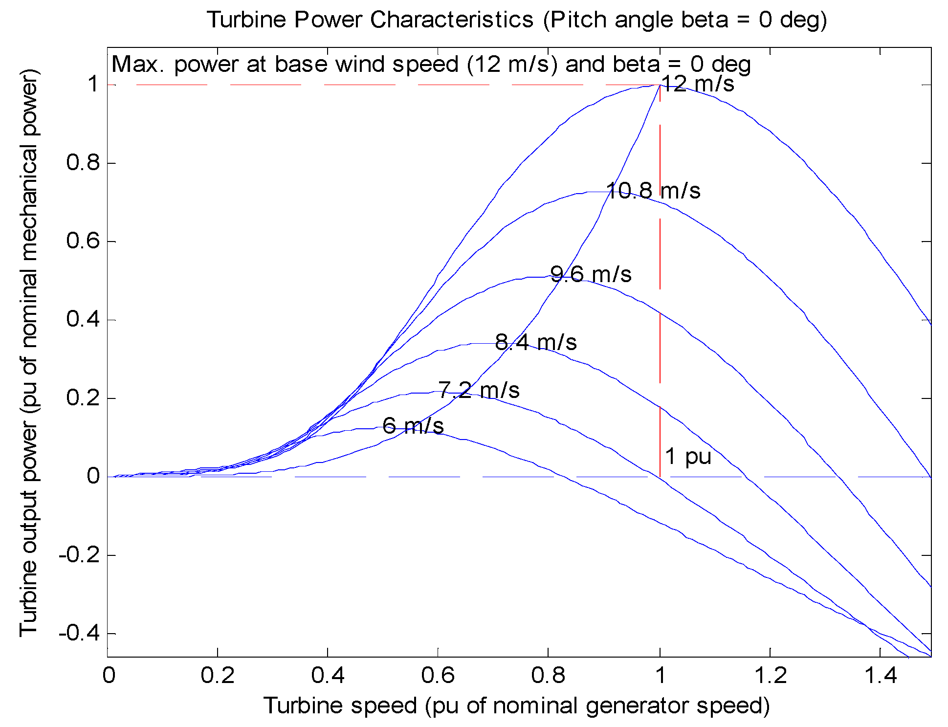
2.3. Wind Turbine and Utility Grid Modelling

2.4. DC Link Voltage Regulation and Grid Side Converter Control
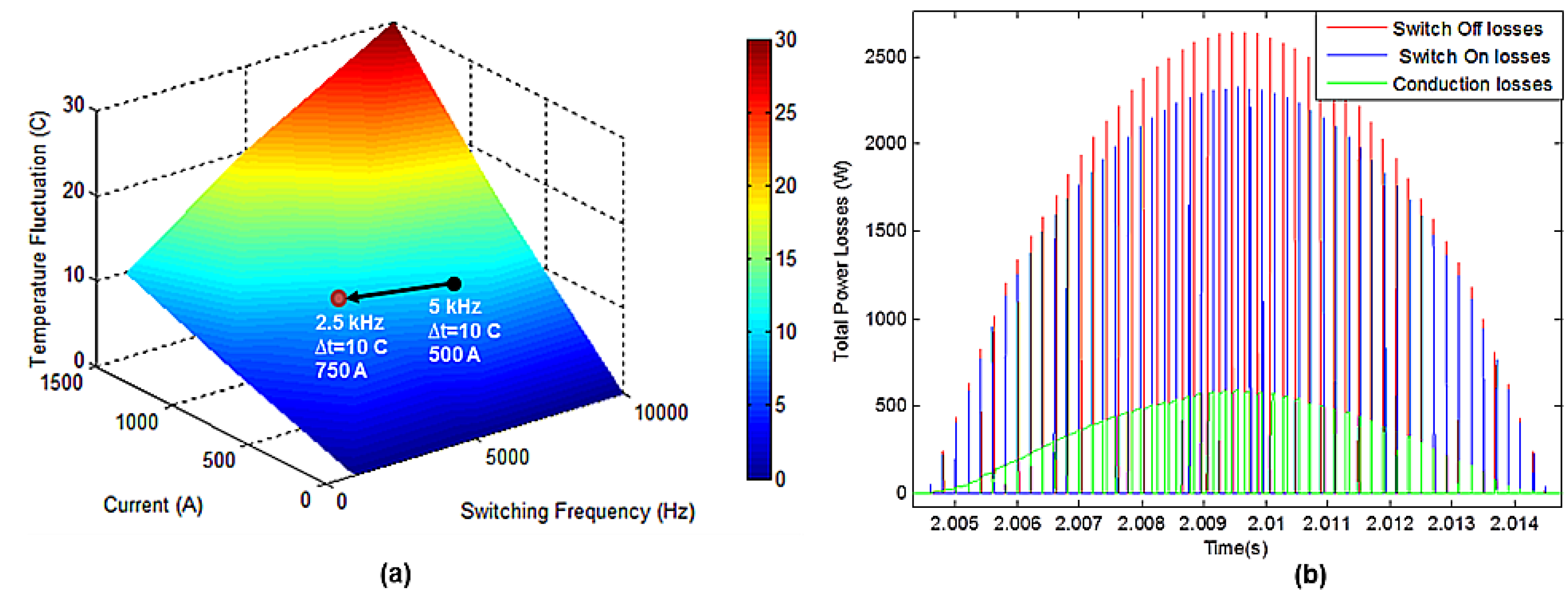
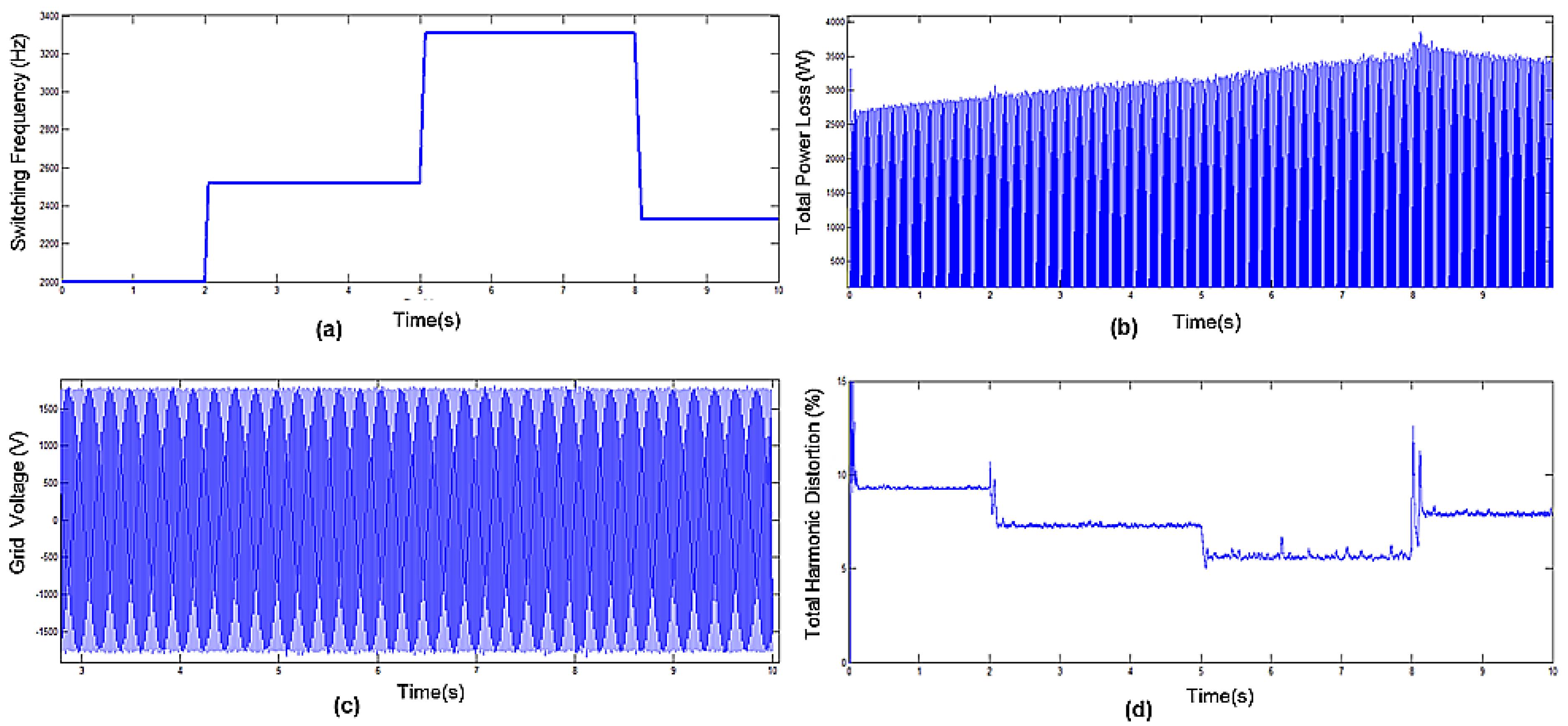
2.5. Generator Side Control with Switching Frequency Regulation

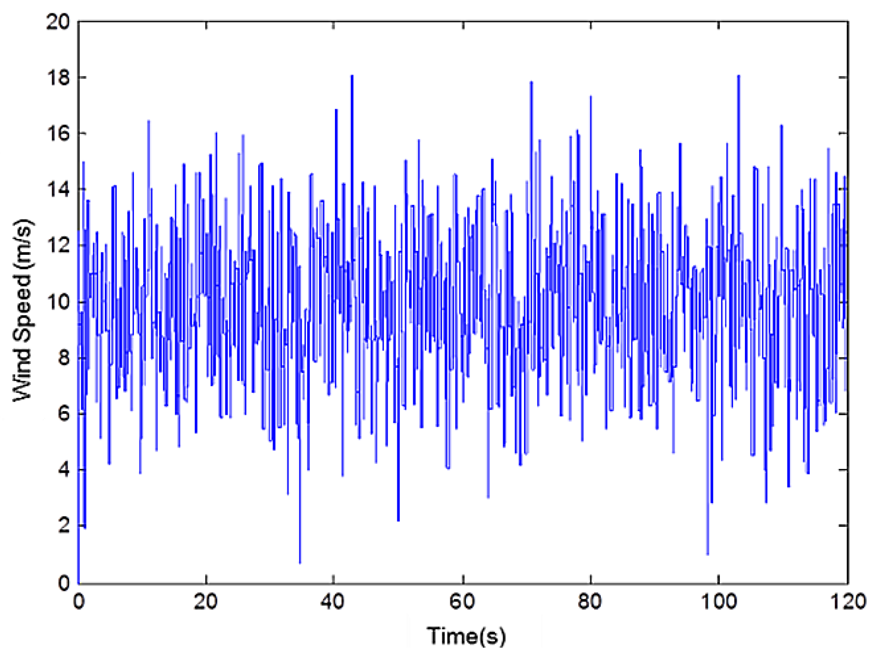
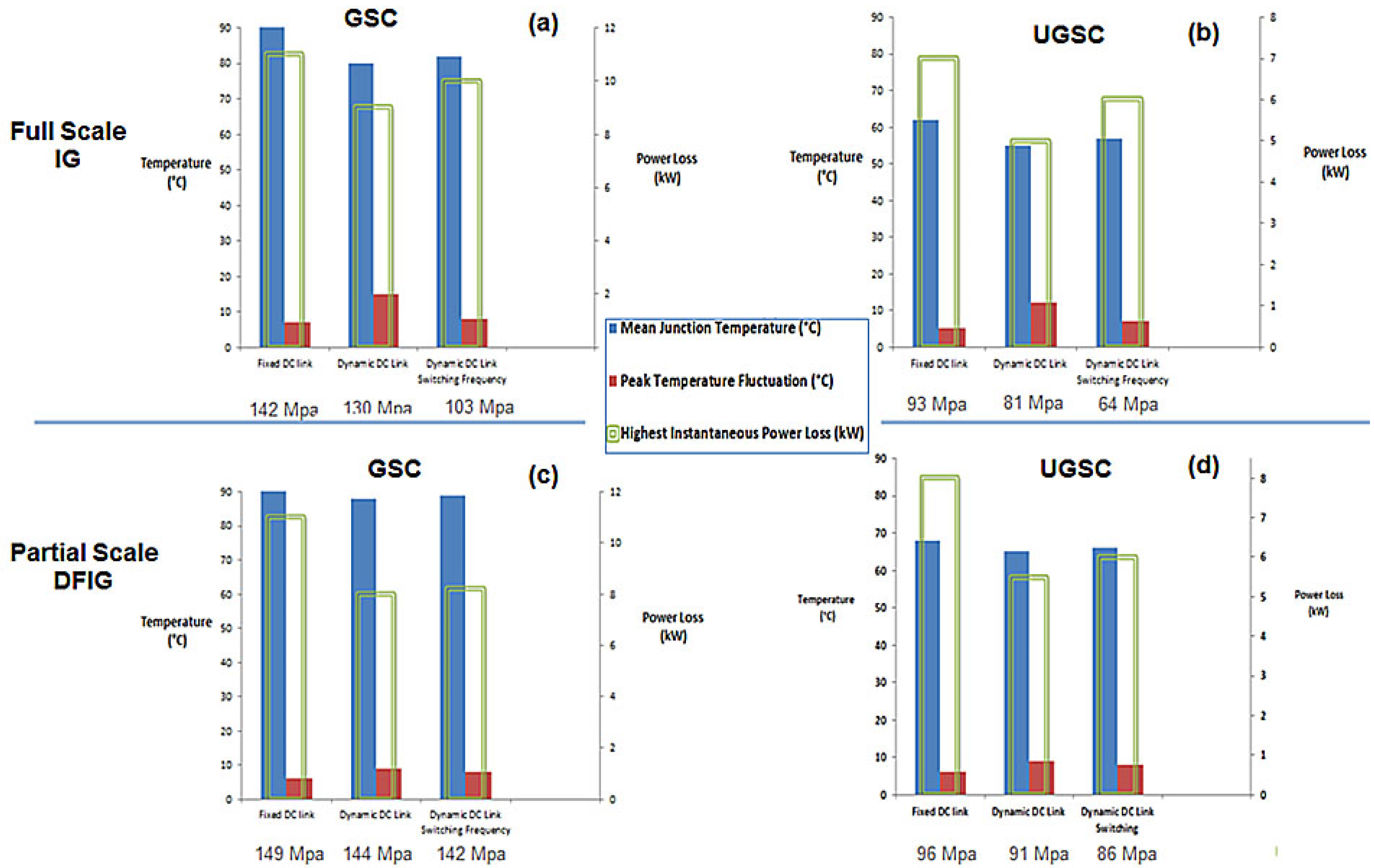
3. Results and Discussion
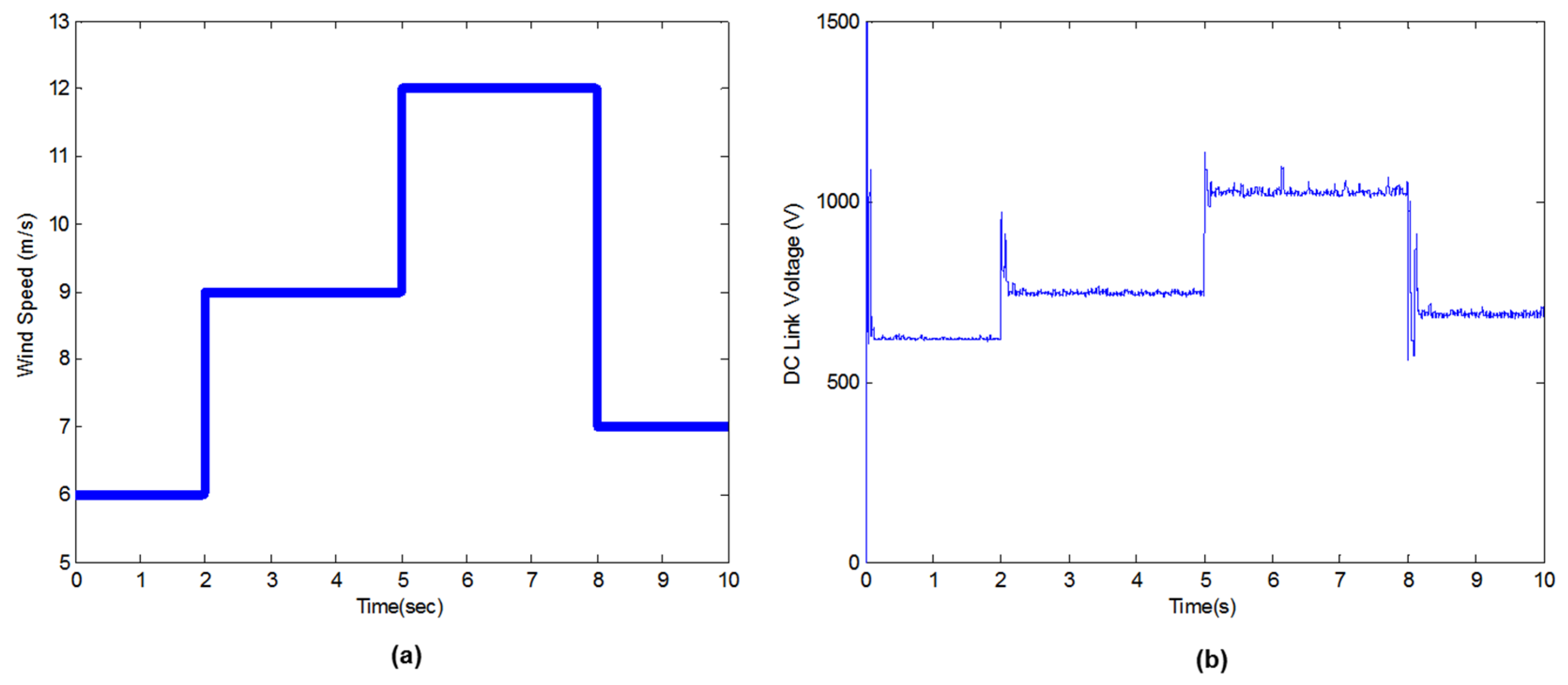
3.1. Dynamic DC Link Voltage and Switching Frequency Analysis


| Layer | Thermal Capacitance | Thermal Resistance | ||||
|---|---|---|---|---|---|---|
| Cth,1 | Cth,2 | Cth,3 | Rth,1 | Rth,2 | Rth,3 | |
| Silicon | 0.48 | 113.14 | 13.78 | 0.217 | 0.056 | 0.061 |
| Solder | 0.69 | 113.31 | 13.92 | 0.212 | 0.055 | 0.058 |
| Copper | 0.85 | 113.62 | 14.22 | 0.198 | 0.054 | 0.057 |
| AIN | 1.02 | 113.94 | 14.88 | 0.175 | 0.053 | 0.056 |
| Copper | 1.57 | 114.31 | 15.31 | 0.154 | 0.053 | 0.056 |
| Solder | 2.01 | 114.78 | 16.04 | 0.136 | 0.052 | 0.052 |
| Baseplate | 6.63 | 115.02 | 430.0 | 0.132 | 0.050 | 0.009 |
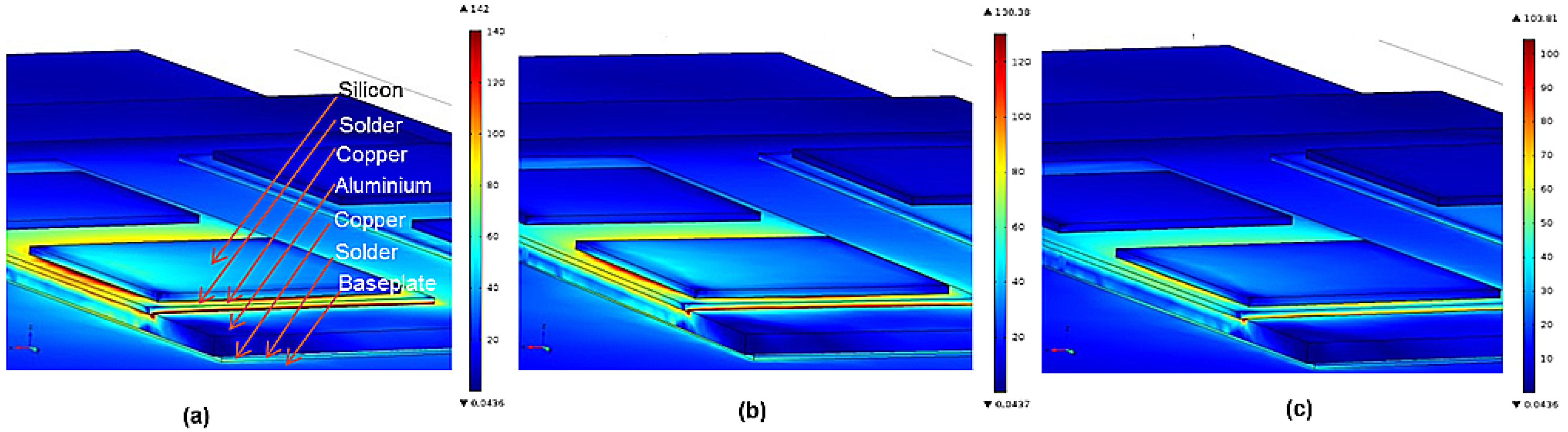
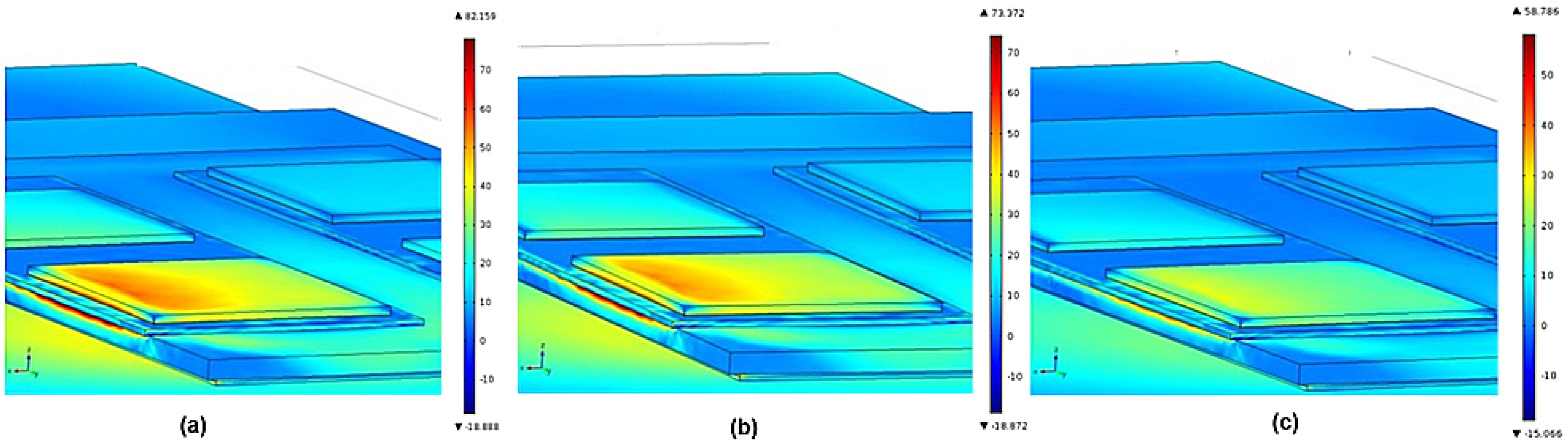
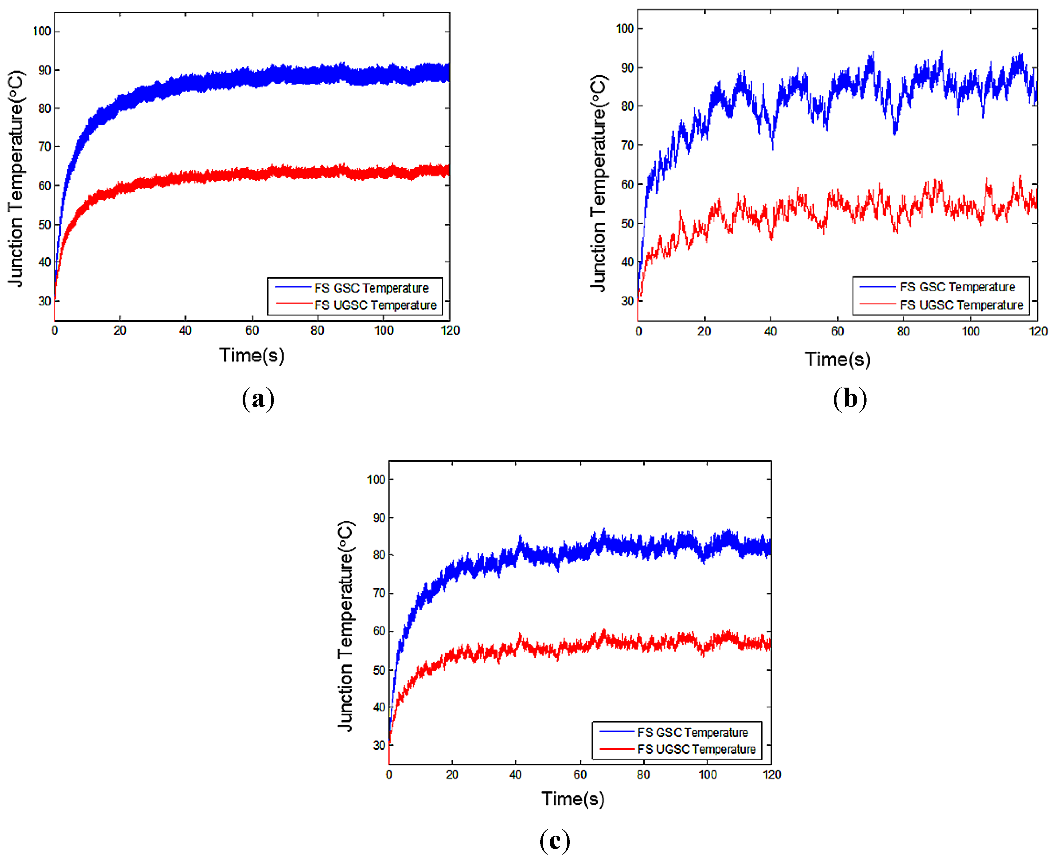
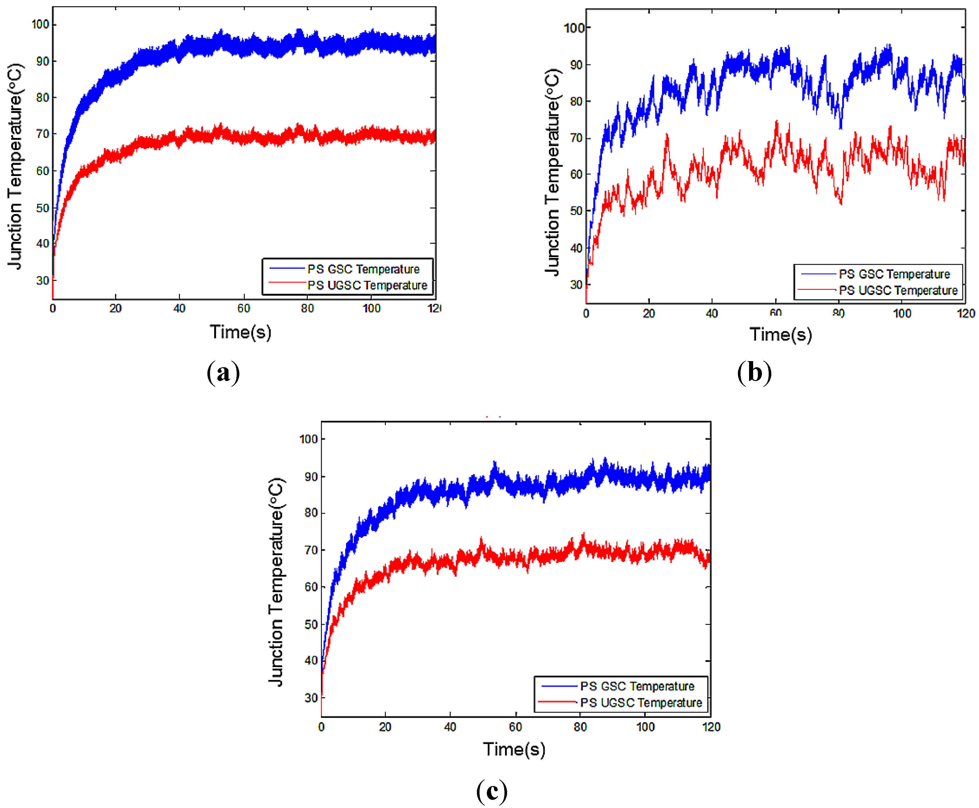
3.2. Comparison of Temperature Profiles for FS and PS Based Back to Back (BTB) PECs

3.3. Thermo-Mechanical Performance of Proposed Model


4. Conclusions
Acknowledgments
Author Contributions
Conflicts of Interest
References
- Blaabjerg, F.; Liserre, M.; Ma, K. Power Electronics Converters for Wind Turbine Systems. IEEE Trans. Ind. Appl. 2012, 48, 708–719. [Google Scholar] [CrossRef]
- Zhou, D.; Blaabjerg, F.; Lau, M.; Tonnes, M. Thermal Cycling Overview of Multi-Megawatt Two-Level Wind Power Converter at Full Grid Code Operation. IEEJ J. Ind. Appl. 2013, 2, 173–182. [Google Scholar] [CrossRef]
- Ensslin, C.; Durstewitz, M.; Hahn, B.; Lange, B.; Rohrig, K. German Wind Energy Report 2008; Available online: http://windmonitor.iwes.fraunhofer.de/img/Wind_energy_report_2008.pdf (accessed on 17 July 2015).
- Lu, H.; Bailey, C.; Yin, C. Design for reliability of power electronics modules. Microelectron. Reliab. 2009, 49, 1250–1255. [Google Scholar] [CrossRef]
- Darwish, A.M.; Bayba, A.; Hung, H.A. FET Gate Length Impact on Reliability. In Proceedings of the IEEE/MTT-S International Microwave Symposium, Honolulu, HI, USA, 3–8 June 2007; pp. 311–314.
- Vermeersch, B.; de Mey, G. A Fixed-Angle Heat Spreading Model for Dynamic Thermal Characterization of Rear-Cooled Substrates. In Proceedings of the Twenty Third Annual IEEE Semiconductor Thermal Measurement and Management Symposium, San Jose, CA, USA, 18–22 March 2007; pp. 95–101.
- Janicki, M.; de Mey, G.; Napieralski, A. Transient thermal analysis of multilayered structures using Green’s functions. Microelectron. Reliab. 2002, 42, 1059–1064. [Google Scholar] [CrossRef]
- Swan, I.; Bryant, A.; Mawby, P. Fast Thermal Models for Power Device Packaging. In Proceedings of the IEEE Industry Applications Society Annual Meeting, Edmonton, AB, Canada, 5–9 October 2008; pp. 1–8.
- Wu, J.; Zhou, L.; Du, X.; Sun, P. Junction Temperature Prediction of IGBT Power Module Based on BP Neural Network. J. Electr. Eng. Technol. 2014, 9, 970–977. [Google Scholar] [CrossRef]
- Skuriat, R.; Johnson, C.M. Thermal performance of baseplate and direct substrate cooled power modules. In Proceedings of the 4th IET Conference on Power Electronics, Machines and Drives, York, UK, 2–4 April 2008; pp. 548–552.
- Huang, H.; Bryant, A.T.; Mawby, P.A. Electro-thermal modelling of three phase inverter. In Proceedings of the 2011—14th European Conference on Power Electronics and Applications, Birmingham, UK, 30 August–1 September 2011; pp. 1–7.
- Ma, K.; Blaabjerg, F. The Impact of Power Switching Devices on the Thermal Performance of a 10 MW Wind Power NPC Converter. Energies 2012, 5, 2559–2577. [Google Scholar] [CrossRef]
- Ma, K.; Blaabjerg, F. Multilevel converters for 10 MW Wind Turbines. In Proceedings of the 2011—14th European Conference on Power Electronics and Applications, Birmingham, UK, 30 August–1 September 2011; pp. 1–10.
- Senturk, O.S.; Helle, L.; Munk-Nielsen, S.; Rodriguez, P.; Teodorescu, R. Converter Structure-Based Power Loss and Static Thermal Modeling of the Press-Pack IGBT Three-Level ANPC VSC Applied to Multi-MW Wind Turbines. IEEE Trans. Ind. Appl. 2011, 47, 2505–2515. [Google Scholar] [CrossRef]
- Blaabjerg, F.; Ma, K.; Zhou, D. Power electronics and reliability in renewable energy systems. In Proceedings of the IEEE International Symposium on Industrial Electronics, Hangzhou, China, 28–31 May 2012; pp. 19–30.
- Lee, J.S.; Lee, K.B. Variable DC-Link Voltage Algorithm with a Wide Range of Maximum Power Point Tracking for a Two-String PV System. Energies 2013, 6, 58–78. [Google Scholar] [CrossRef]
- Gao, F.; Li, D.; Loh, P.C.; Tang, Y.; Wang, P. Indirect dc-link voltage control of two-stage single-phase PV inverter. In Proceedings of the IEEE Energy Conversion Congress and Exposition, San Jose, CA, USA, 20–24 September 2009; pp. 1166–1172.
- Zou, Y.; Elbuluk, M.; Sozer, Y. Stability analysis of maximum power point tracking (MPPT) method in wind power systems. In Proceedings of the IEEE Industry Applications Society Annual Meeting (IAS), Orlando, FL, USA, 9–13 October 2011; pp. 1–8.
- Han, K.; Chen, G. A novel control strategy of wind turbine MPPT implementation for direct-drive PMSG wind generation imitation platform. In Proceedings of the Power Electronics and Motion Control Conference, IPEMC 6th Int IEEE, Wuhan, China, 17–20 May 2009; pp. 2255–2259.
- El-Sousy, F.F.M.; Orabi, M.; Godah, H. Maximum Power Point Tracking Control Scheme for Grid Connected Variable Speed Wind Driven Self-Excited Induction Generator. J. Power Electron. 2006, 6, 52–66. [Google Scholar]
- Bekakra, Y.; Attous, D.B. DFIG sliding mode control fed by back-to-back PWM converter with DC-link voltage control for variable speed wind turbine. Front Energy 2014, 8, 345–354. [Google Scholar] [CrossRef]
- Dayaratne, U.I.; Tennakoon, S.B.; Shammas, N.Y.A.; Knight, J.S. Investigation of variable DC link voltage operation of a PMSG based wind turbine with fully rated converters at steady state. In Proceedings of the 14th European Conference on Power Electronics and Applications (EPE), Birmingham, UK, 30 August–1 September 2011; pp. 1–10.
- Yu, C.Y.; Tamura, J.; Lorenz, R.D. Control method for calculating optimum DC bus voltage to improve drive system efficiency in variable DC bus drive systems. In Proceedings of the IEEE Energy Conversion Congress and Exposition (ECCE), Raleigh, NC, USA, 15–20 September 2012; pp. 2992–2999.
- Pei, X.; Kang, Y.; Chen, J. Analysis and calculation of DC-link current and voltage ripple for three-phase inverter with unbalanced loads. In Proceedings of the Twenty-Ninth Annual IEEE Applied Power Electronics Conference and Exposition, Fort Worth, TX, USA, 19–20 March 2014; pp. 1565–1572.
- Lemmens, J.; Driesen, J.; Vanassche, P. Thermal management in traction applications as a constraint optimal control problem. In Proceedings of the IEEE Vehicle Power and Propulsion Conference (VPPC), Seoul, South Korea, 9–12 October 2012; pp. 36–41.
- Andresen, M.; Liserre, M. Impact of active thermal management on power electronics design. Microelectron. Reliab. 2014, 54, 1935–1939. [Google Scholar] [CrossRef]
- Ma, K.; Blaabjerg, F. Reliability-cost models for the power switching devices of wind power converters. In Proceedings of the 3rd IEEE International Symposium on Power Electronics for Distributed Generation Systems (PEDG), Aalborg, Denmark, 25–28 June 2012; pp. 820–827.
- Ma, K.; Bahman, A.S.; Beczkowski, S.; Blaabjerg, F. Complete Loss and Thermal Model of Power Semiconductors Including Device Rating Information. IEEE Trans. Power Electron. 2015, 5, 2556–2569. [Google Scholar] [CrossRef]
- Kuhn, H.; Mertens, A. On-line junction temperature measurement of IGBTs based on temperature sensitive electrical parameters. In Proceedings of the 13th European Conference on Power Electronics and Applications, Barcelona, Spanish, 8–10 September 2009; pp. 1–10.
- Mysore, K.; Subbarayan, G.; Gupta, V.; Zhang, R. Constitutive and Aging Behavior of Sn3.0Ag0.5Cu Solder Alloy. IEEE Trans. Electron. Packag. Manuf. 2009, 32, 221–232. [Google Scholar] [CrossRef]
- Liu, Y. Power Electronic Packaging: Design, Assembly Process, Reliability and Modeling; Springer Science & Business Media: New York, NY, USA, 2012; pp. 3–7. [Google Scholar]
- Online Materials Information Resource. Available online: http://www.matweb.com/ (accessed on 15 July 2015).
- Shaoyong, Y.; Bryant, A.; Mawby, P.; Dawei, X.; Li, R.; Tavner, P. An Industry-Based Survey of Reliability in Power Electronic Converters. IEEE Trans. Ind. Appl. 2011, 47, 1441–1451. [Google Scholar]
- Drofenik, U.; Cottet, D.; Müsing, A.; Meyer, J.; Kolar, J.W. Modelling the Thermal Coupling between Internal Power Semiconductor Dies of a Water-Cooled 3300 V/1200 A HiPak IGBT Module. In Proceedings of the Conference for Power Electronics, Intelligent Motion, Power Quality, Nuremberg, Germany, 22–24 May 2007; pp. 22–24.
- Ye, H.; Lin, M.; Basaran, C. Failure modes and FEM analysis of power electronic packaging. Finite Elem. Anal. Des. 2002, 38, 601–612. [Google Scholar] [CrossRef]
- Xu, L.; Liu, Y.; Liu, S. Modeling and simulation of power electronic modules with microchannel coolers for thermo-mechanical performance. Microelectron. Reliab. 2014, 54, 2824–2835. [Google Scholar] [CrossRef]
- Anand, L. Constitutive Equations for the Rate-Dependent Deformation of Metals at Elevated Temperatures. J. Eng. Mater. Technol. 1982, 104, 12–17. [Google Scholar] [CrossRef]
- Mohan, N. Advanced Electric Drives: Analysis, Control, and Modeling Using MATLAB/Simulink; John Wiley & Sons: Hoboken, NJ, USA, 2014; pp. 28–37. [Google Scholar]
- Kaźmierkowski, M.P.; Krishnan, R.; Blaabjerg, F. Control in Power Electronics: Selected Problems; Academic Press: Amsterdam, NY, USA, 2002; pp. 434–435. [Google Scholar]
© 2015 by the authors; licensee MDPI, Basel, Switzerland. This article is an open access article distributed under the terms and conditions of the Creative Commons Attribution license (http://creativecommons.org/licenses/by/4.0/).
Share and Cite
Batunlu, C.; Albarbar, A. A Technique for Mitigating Thermal Stress and Extending Life Cycle of Power Electronic Converters Used for Wind Turbines. Electronics 2015, 4, 947-968. https://doi.org/10.3390/electronics4040947
Batunlu C, Albarbar A. A Technique for Mitigating Thermal Stress and Extending Life Cycle of Power Electronic Converters Used for Wind Turbines. Electronics. 2015; 4(4):947-968. https://doi.org/10.3390/electronics4040947
Chicago/Turabian StyleBatunlu, Canras, and Alhussein Albarbar. 2015. "A Technique for Mitigating Thermal Stress and Extending Life Cycle of Power Electronic Converters Used for Wind Turbines" Electronics 4, no. 4: 947-968. https://doi.org/10.3390/electronics4040947