
Homogeneous Crystallization of Micro-DispensedTIPS-Pentacene Using a Two-Solvent System toEnable Printed Inverters on Foil Substrates

Abstract
:
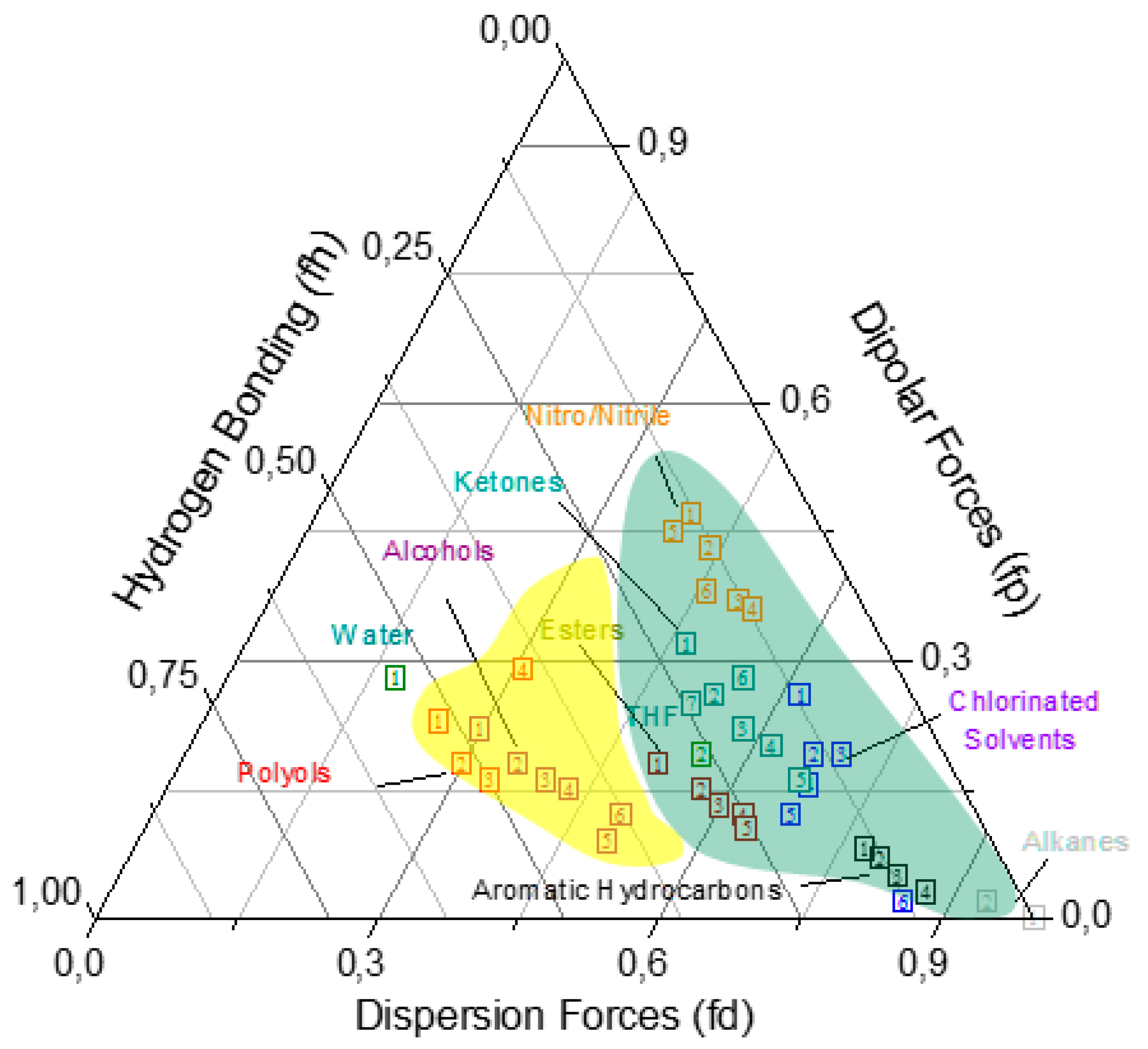
1. Introduction
2. Two-Solvent Optimization Process and Its Results
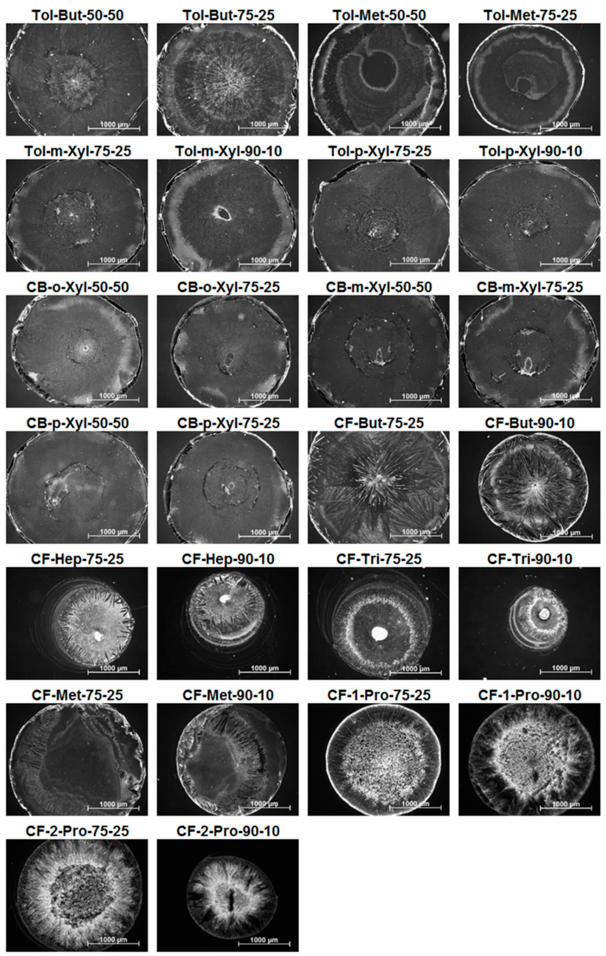
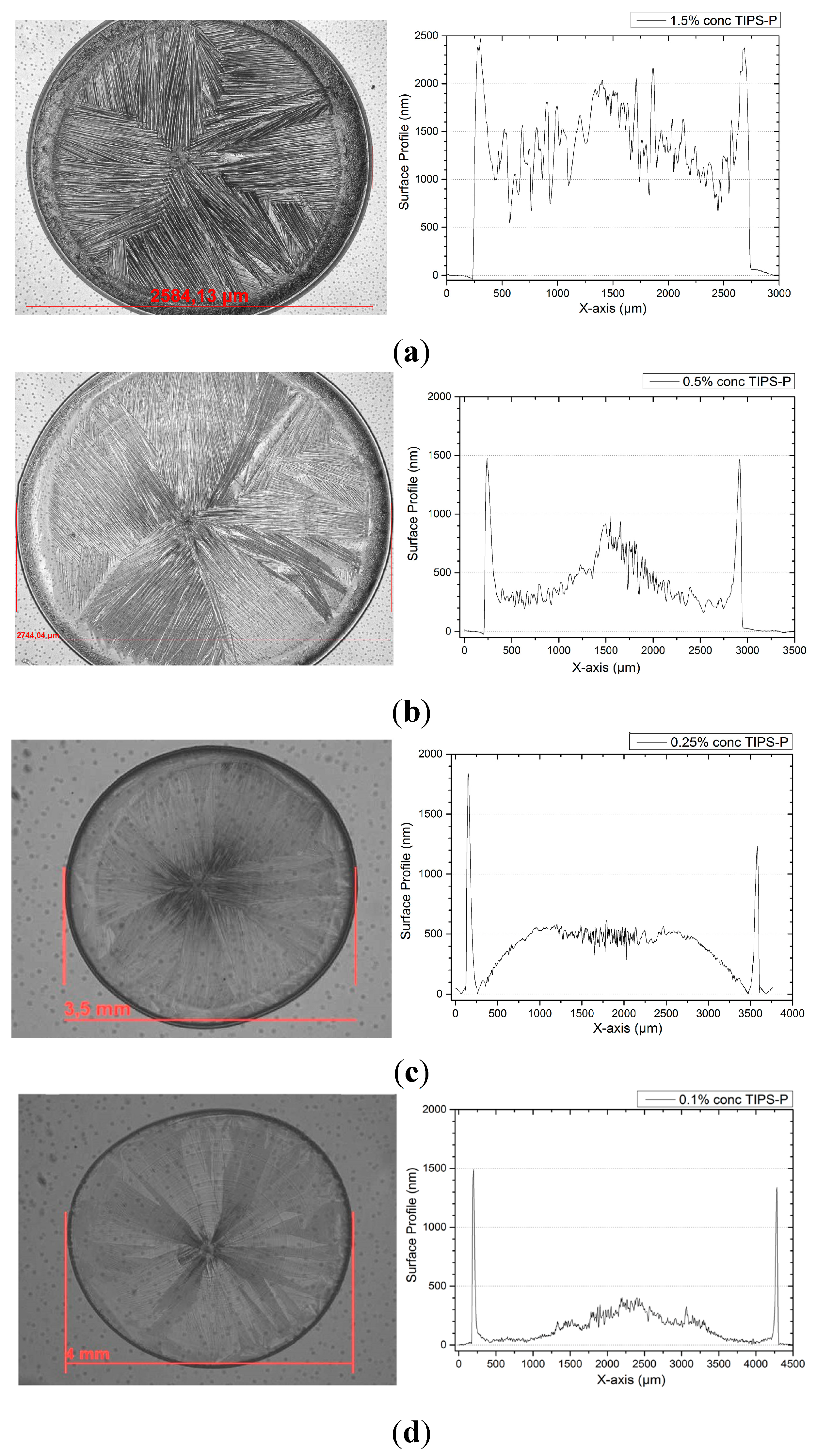
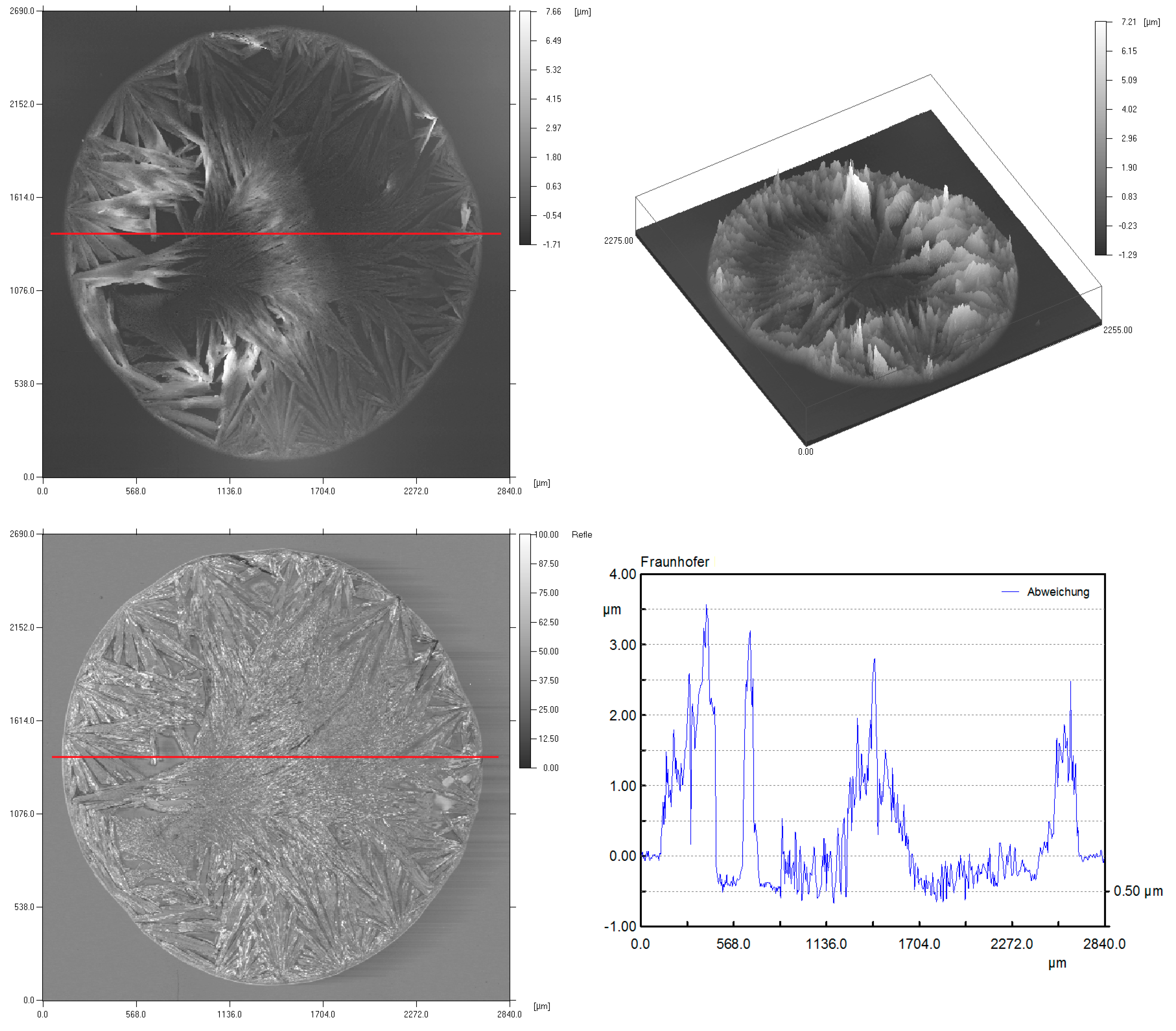
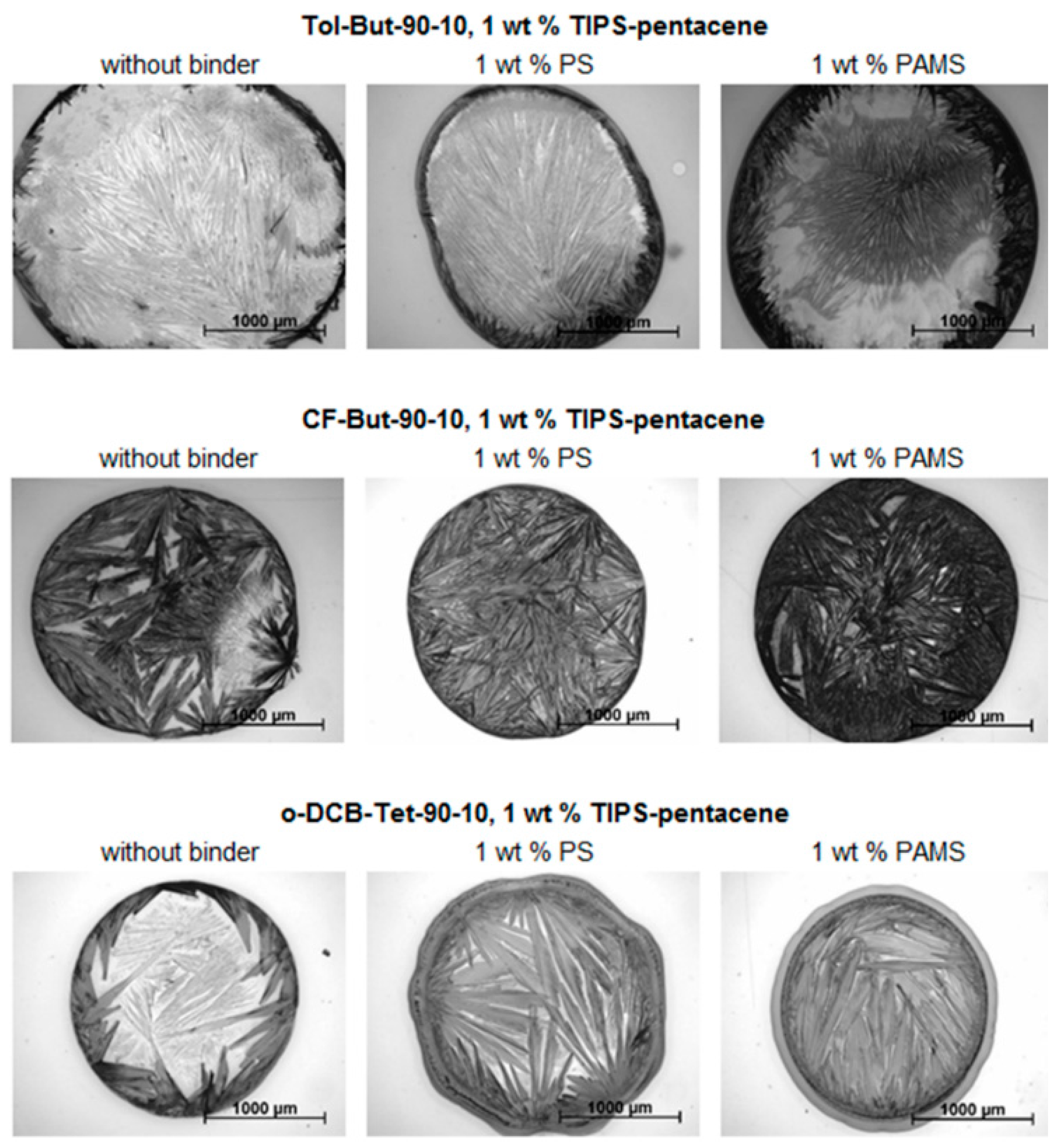
2.1. Experimental Part I


| # | Major Solvent | Boiling Point (°C) | Minor Solvent | Boiling Point (°C) | Ratio | Short Name |
|---|---|---|---|---|---|---|
| A1 | Toluene | 111 °C | n-Butyl acetate | 126 °C | 50%–50% | Tol-But-50-50 |
| A2 | Toluene | n-Butyl acetate | 75%–25% | Tol-But-75-25 | ||
| A3 | Toluene | 4-Methyl-2-pentanone | 117 °C | 50%–50% | Tol-Met-50-50 | |
| A4 | Toluene | 4-Methyl-2-pentanone | 75%–25% | Tol-Met-75-25 | ||
| A5 | Toluene | m-Xylene | 139 °C | 75%–25% | Tol-m-Xyl-75-25 | |
| A6 | Toluene | m-Xylene | 90%–10% | Tol-m-Xyl-90-10 | ||
| A7 | Toluene | p-Xylene | 138 °C | 75%–25% | Tol-p-Xyl-75-25 | |
| A8 | Toluene | p-Xylene | 90%–10% | Tol-p-Xyl-90-10 | ||
| B1 | Chlorobenzene | 132 °C | o-Xylene | 144 °C | 50%–50% | CB-o-Xyl-50-50 |
| B2 | Chlorobenzene | o-Xylene | 75%–25% | CB-o-Xyl-75-25 | ||
| B3 | Chlorobenzene | m-Xylene | 139 °C | 50%–50% | CB-m-Xyl-50-50 | |
| B4 | Chlorobenzene | m-Xylene | 75%–25% | CB-m-Xyl-75-25 | ||
| B5 | Chlorobenzene | p-Xylene | 138 °C | 50%–50% | CB-p-Xyl-50-50 | |
| B6 | Chlorobenzene | p-Xylene | 75%–25% | CB-p-Xyl-75-25 | ||
| C1 | Chloroform | 61 °C | n-Butyl acetate | 126 °C | 75%–25% | CF-But-75-25 |
| C2 | Chloroform | n-Butyl acetate | 90%–10% | CF-But-90-10 | ||
| C3 | Chloroform | Heptane | 98 °C | 75%–25% | CF-Hep-75-25 | |
| C4 | Chloroform | Heptane | 90%–10% | CF-Hep-90-10 | ||
| C5 | Chloroform | 2,2,4-Trimethylpentane | 99 °C | 75%–25% | CF-Tri-75-25 | |
| C6 | Chloroform | 2,2,4-Trimethylpentane | 90%–10% | CF-Tri-90-10 | ||
| C7 | Chloroform | 4-Methyl-2-pentanone | 117 °C | 75%–25% | CF-Met-75-25 | |
| C8 | Chloroform | 4-Methyl-2-pentanone | 90%–10% | CF-Met-90-10 | ||
| D1 | Chloroform | 61 °C | 1-Propanol | 97 °C | 75%–25% | CF-1-Pro-75-25 |
| D2 | Chloroform | 1-Propanol | 90%–10% | CF-1-Pro-90-10 | ||
| D3 | Chloroform | 2-Propanol | 82 °C | 75%–25% | CF-2-Pro-75-25 | |
| D4 | Chloroform | 2-Propanol | 90%–10% | CF-2-Pro-90-10 |
2.2. Experimental Part II
| # | Major Solvent | Boiling Point (°C) | Minor Solvent | Boiling Point (°C) | Ratio | Short Name |
|---|---|---|---|---|---|---|
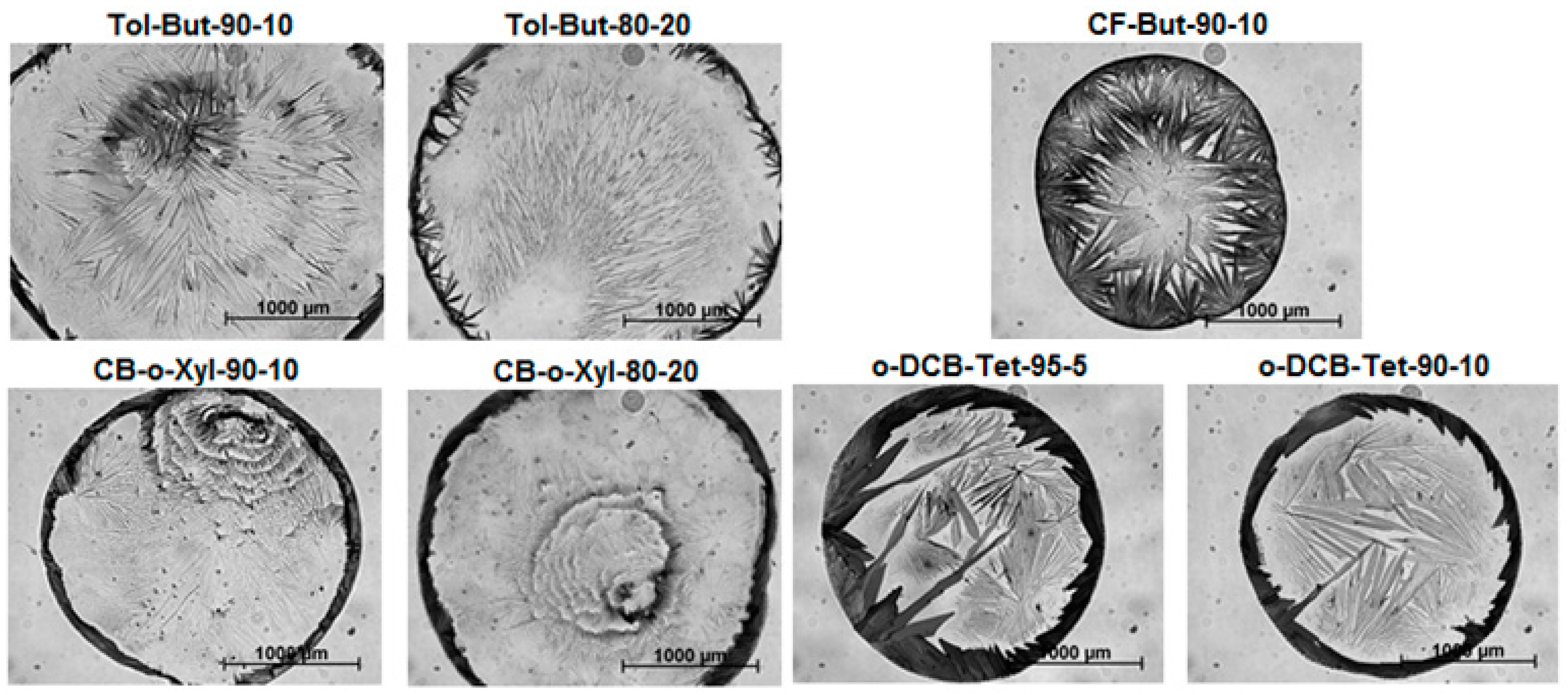
| A1 | Toluene | 111 °C | n-Butyl acetate | 126 °C | 90%–10% | Tol-But-90-10 |
| A2 | Toluene | n-Butyl acetate | 80%–20% | Tol-But-80-20 | ||
| B1 | Chlorobenzene | 132 °C | o-Xylene | 144 °C | 90%–10% | CB-o-Xyl-90-10 |
| B2 | Chlorobenzene | o-Xylene | 80%–20% | CB-o-Xyl-80-20 | ||
| C1 | Chloroform | 61 °C | n-Butyl acetate | 126 °C | 90%–10% | CF-But-90-10 |
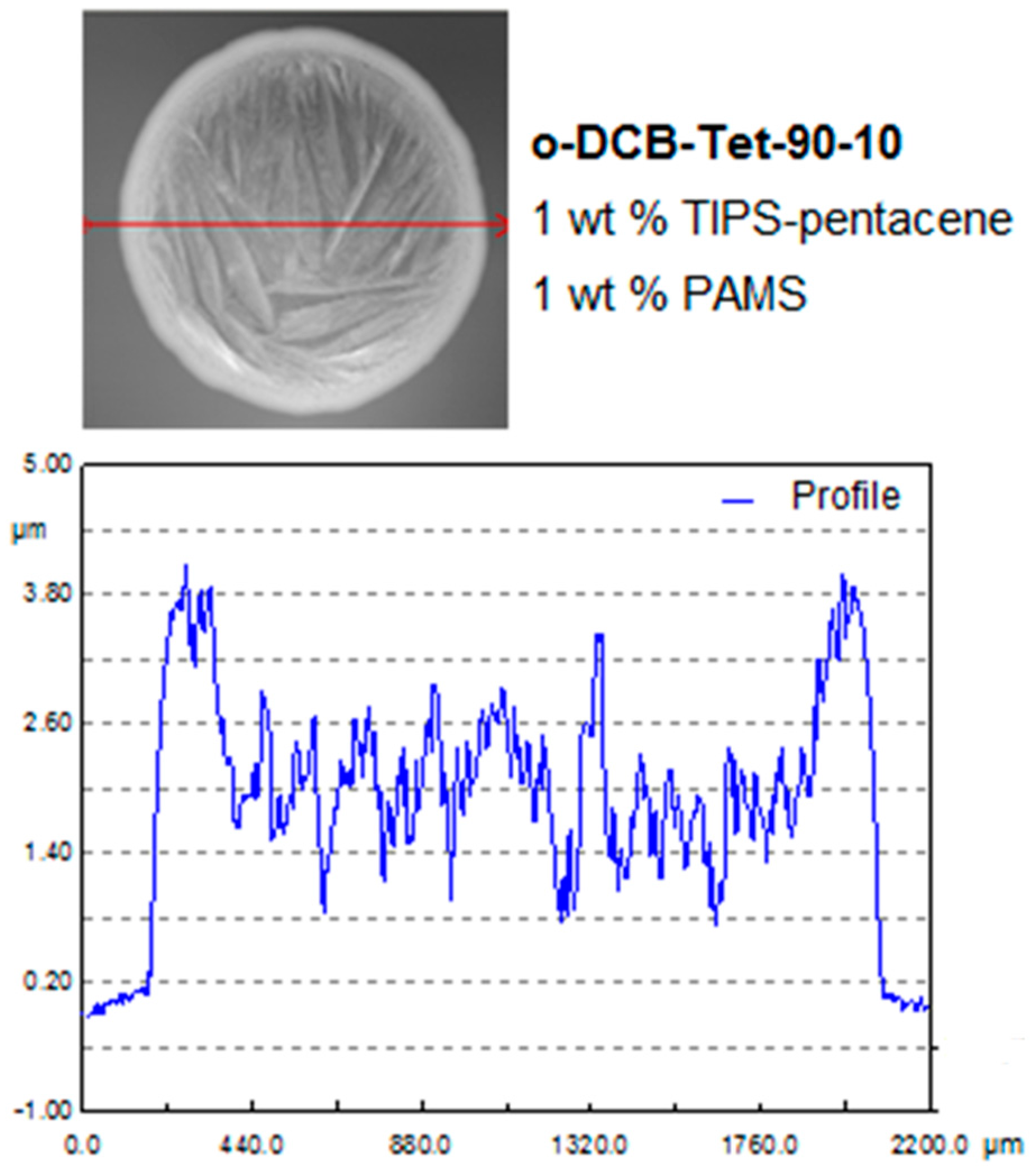
| D1 | o-Dichlorobenzene | 180 °C | Tetralin | 207 °C | 95%–5% | o-DCB-Tet-95-5 |
| D2 | o-Dichlorobenzene | Tetralin | 90%–10% | o-DCB-Tet-90-10 |
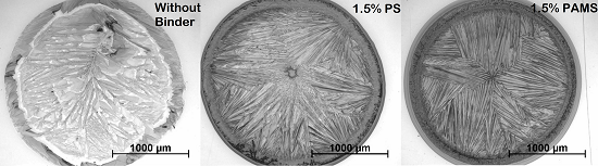
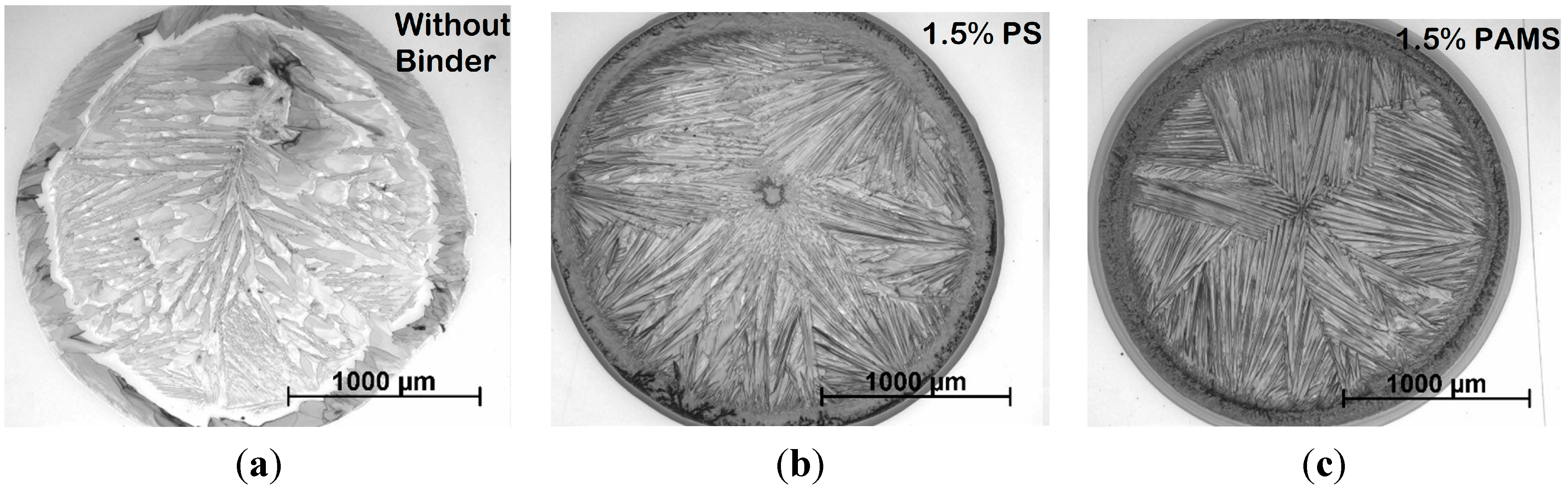
2.3. Experimental Part III
| # | Major Solvent | Boiling Point (°C) | Minor Solvent | Boiling Point (°C) | Ratio | TIPS-pentacene | Binder |
|---|---|---|---|---|---|---|---|
| A1 | Toluene | 111 °C | n-Butyl acetate | 126 °C | 90%–10% | 1% | None |
| A1_PS | Toluene | n-Butyl acetate | 90%–10% | 1% | PS (1% wt) | ||
| A1_PAMS | Toluene | n-Butyl acetate | 90%–10% | 1% | PAMS (1% wt) | ||
| C1 | Chloroform | 61 °C | n-Butyl acetate | 126 °C | 90%–10% | 1% | None |
| C1_PS | Chloroform | n-Butyl acetate | 90%–10% | 1% | PS (1% wt) | ||
| C1_PAMS | Chloroform | n-Butyl acetate | 90%–10% | 1% | PAMS (1% wt) | ||
| D1 | o-Dichloro benzene | 180 °C | Tetralin | 207 °C | 90%–10% | 1% | None |
| D1_PS | o-Dichloro benzene | Tetralin | 90%–10% | 1% | PS (1% wt) | ||
| D1_PAMS | o-Dichloro benzene | Tetralin | 90%–10% | 1% | PAMS (1% wt) |
2.4. Experimental Part IV
| Type | Name | Boiling Point (°C) | Surface Tension @ 20 °C (dyn/cm) |
|---|---|---|---|
| Major Solvent (75%) | o-Xylene | 144.4 | 30.53 |
| Minor Solvent (25%) | o-Dichlorobenzene | 180.5 | 37 |


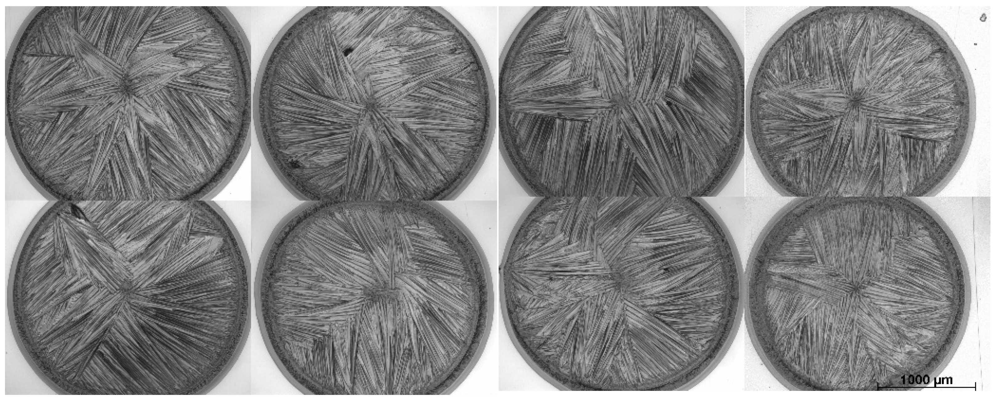
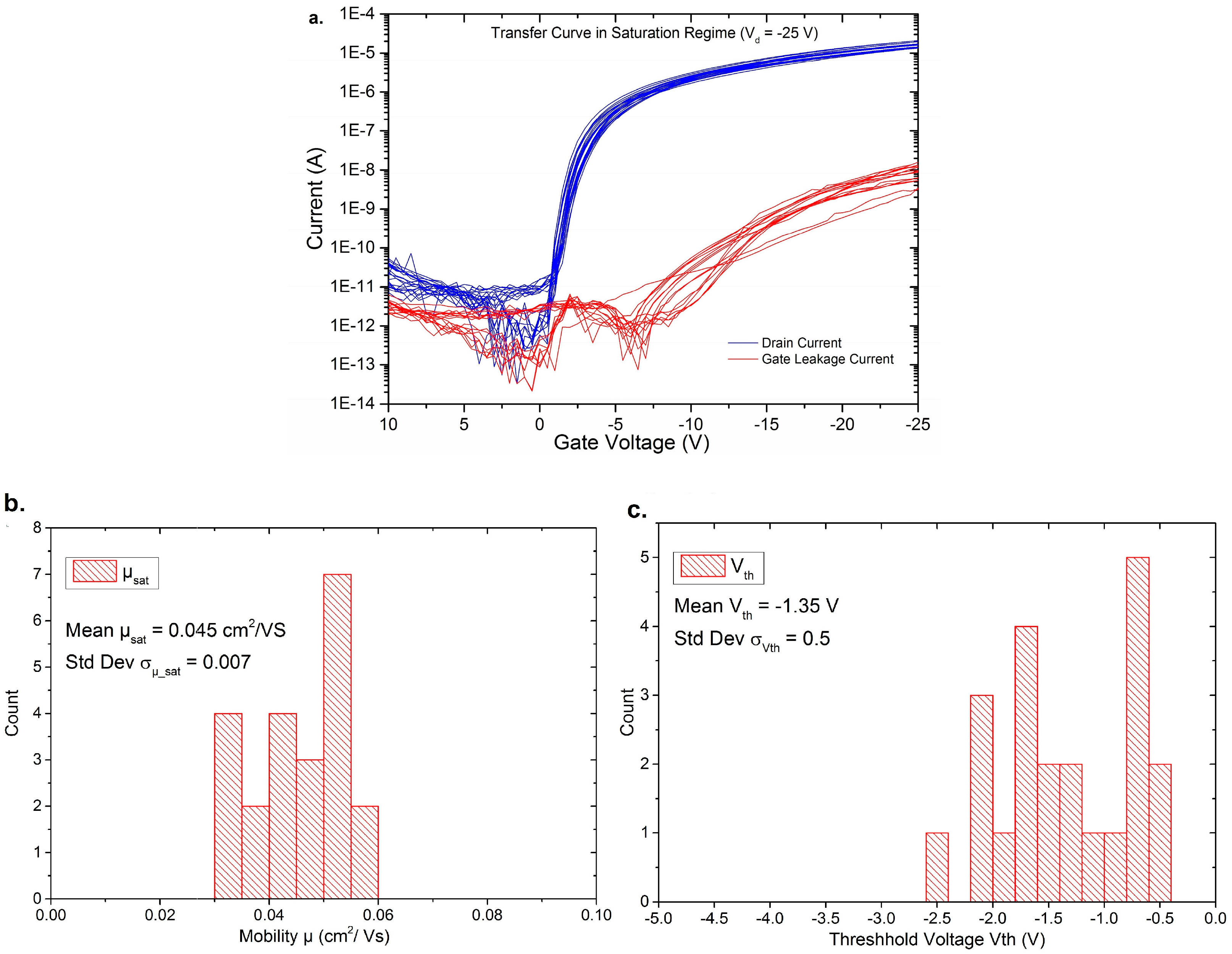
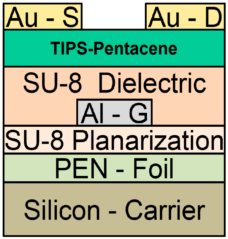
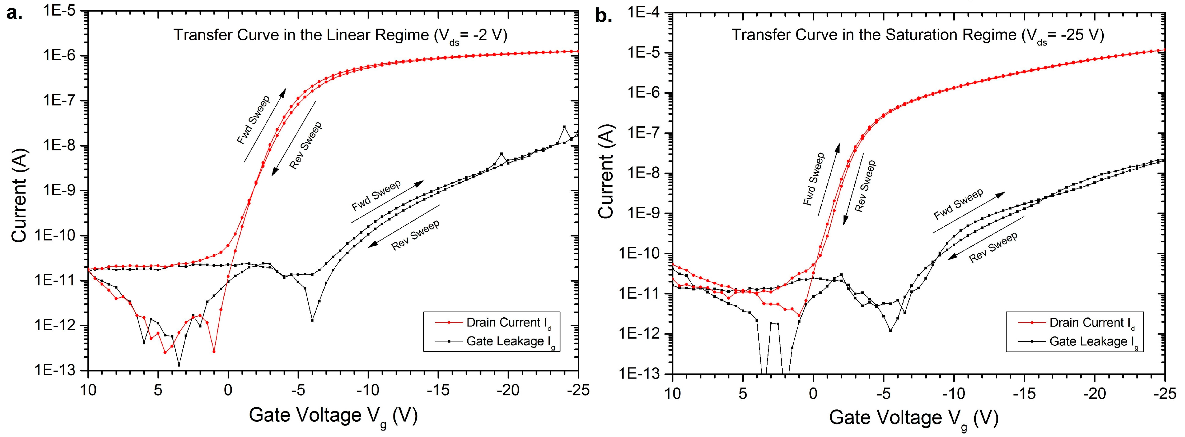
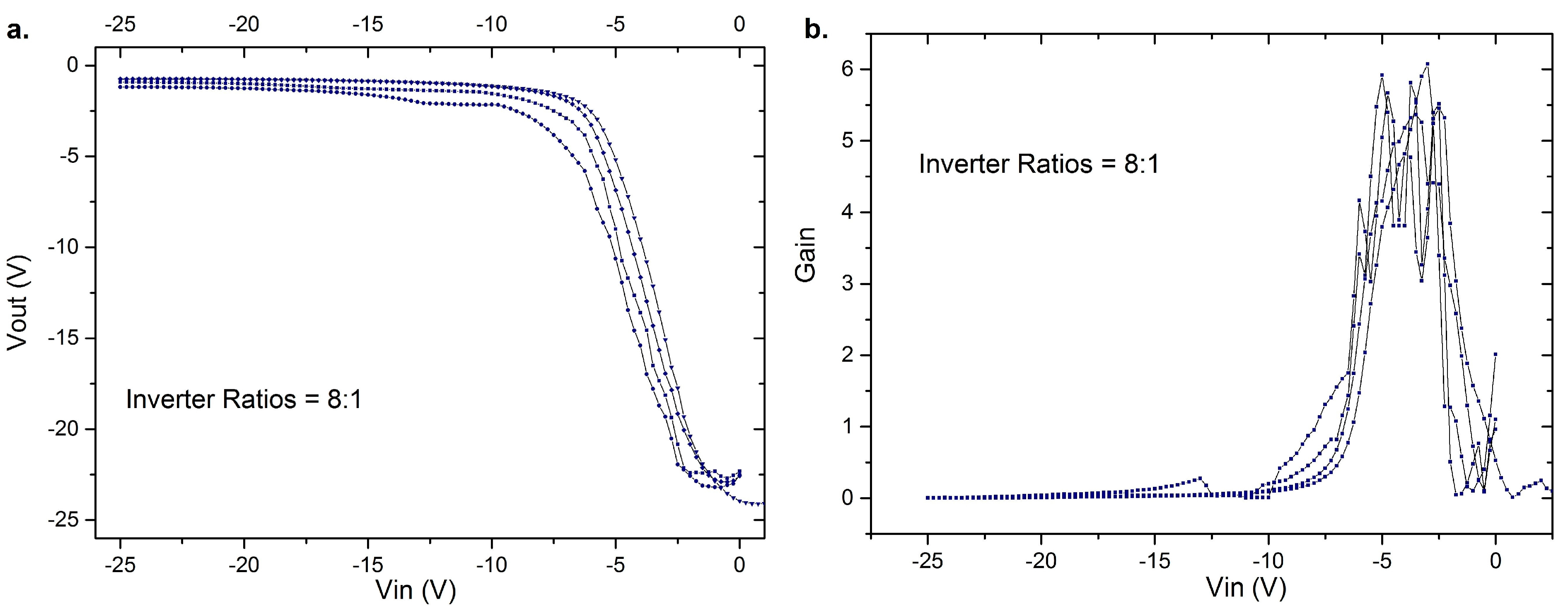
3. Results of the OFETs

4. Conclusions
Acknowledgments
Author Contributions
Conflicts of Interest
References
- Kawase, T.; Moriya, S.; Newsome, C.J.; Shimoda, T. Inkjet printing of polymeric field-effect transistors and its applications. Jpn. J. Appl. Phys. Part 1 2005, 44. [Google Scholar] [CrossRef]
- De Gans, B.J.; Duineveld, P.C.; Schubert, U.S. Inkjet printing of polymers: State of the art and future developments. Adv. Mater. 2004, 16, 203–213. [Google Scholar] [CrossRef]
- Kippelen, B. Advancing consumer packaging through printable electronics. In Proceedings of the IPST Executive Conference, Atlanta, GA, USA, 9–10 March 2011.
- Sekitani, T.; Zschieschang, U.; Klauk, H.; Someya, T. Flexible organic transistors and circuits with extreme bending stability. Nat. Mater. 2010, 9, 1015–1022. [Google Scholar] [CrossRef] [PubMed]
- Park, S.K.; Anthony, J.E.; Jackson, T.N. Solution-processed TIPS-pentacene organic thin-film-transistor circuits. IEEE Electron Device Lett. 2007, 28, 877–879. [Google Scholar] [CrossRef]
- Ohe, T.; Kuribayashi, M.; Yasuda, R.; Tsuboi, A.; Nomoto, K.; Satori, K.; Itabashi, M.; Kasahara, J. Solution-processed organic thin-film transistors with vertical nanophase separation. Appl. Phys. Lett. 2008, 93. [Google Scholar] [CrossRef]
- Hwang, D.K.; Fuentes-Hernandez, C.; Berrigan, J.D.; Fang, Y.; Kim, J.; Potscavage, W.J.; Cheun, H.; Sandhage, K.H.; Kippelen, B. Solvent and polymer matrix effects on TIPS-pentacene/polymer blend organic field-effect transistors. J. Mater. Chem. 2012, 22, 5531–5537. [Google Scholar] [CrossRef]
- Plötner, M.; Wegener, T.; Richter, S.; Howitz, S.; Fischer, W.J. Investigation of ink-jet printing of poly-3-octylthiophene for organic field-effect transistors from different solutions. Synth. Met. 2004, 147, 299–303. [Google Scholar] [CrossRef]
- Volkman, S.K.; Molesa, S.; Mattis, B.; Chang, P.C.; Subramanian, V. Inkjetted organic transistors using a novel pentacene precursor. Mater. Res. Soc. Symp. Proc. 2003, 771. [Google Scholar] [CrossRef]
- Chang, P.C.; Molesa, S.E.; Murphy, A.R.; Frechet, J.M.J.; Subra manian, V. Inkjetted Crystalline Single-Monolayer Oligothiophene OTFTs. IEEE Trans. Electron Devices 2006, 53, 594. [Google Scholar] [CrossRef]
- Lim, J.A.; Lee, W.H.; Lee, H.S.; Lee, J.H.; Park, Y.D.; Cho, K. Self-organization of ink-jet-printed triisopropylsilylethynyl pentacene via evaporation-induced flows in a drying droplet. Adv. Funct. Mater. 2008, 18, 229–234. [Google Scholar] [CrossRef]
- Lada, M.; Starink, M.J.; Carrasco, M.; Chen, L.; Miskiewicz, P.; Brookes, P.; Obarowska, M.; Smith, D.C. Morphology control via dual solvent crystallization for high-mobility functionalized pentacene-blend thin film transistors. J. Mater. Chem. 2011, 21, 11232–11238. [Google Scholar] [CrossRef]
- Chae, G.J.; Jeong, S.H.; Baek, J.H.; Walker, B.; Song, C.K.; Seo, J.H. Improved performance in TIPS-pentacene field effect transistors using solvent additives. J. Mater. Chem. C 2013, 1, 4216–4221. [Google Scholar] [CrossRef] [Green Version]
- Deegan, R.D. Pattern formation in drying drops. Phys. Rev. E 2000, 61. [Google Scholar] [CrossRef]
- Deegan, R.D.; Bakajin, O.; Dupont, T.F.; Huber, G.; Nagel, S.R.; Witten, T.A. Capillary flow as the cause of ring stains from dried liquid drops. Nature 1997, 389, 827–829. [Google Scholar] [CrossRef]
- Tekin, E.; Smith, P.J.; Hoeppener, S.; van den Berg, A.M.J.; Susha, A.S.; Rogach, A.L.; Feldmann, J.; Schubert, U.S. Inkjet Printing of Luminescent CdTe Nanocrystal–Polymer Composites. Adv. Funct. Mater. 2007, 17, 23–28. [Google Scholar] [CrossRef]
- Arias, A.C.; Daniel, J.; Krusor, B.; Ready, S.; Sholin, V.; Street, R. All-additive ink-jet-printed display backplanes: Materials development and integration. J. Soc. Inform. Display 2007, 15, 485–490. [Google Scholar] [CrossRef]
- NanoFokus. Available online: https://www.nanofocus.de/produkte/uscan/mscan-custom/ (accessed on 13 August 2015).
- Tetzner, K.; Bose, I.; Bock, K. Organic field-effect transistors based on a liquid-crystalline polymeric semi-conductor using SU-8 gate dielectrics on flexible substrates. Mater. 2014, 7, 7226–7242. [Google Scholar] [CrossRef]
© 2015 by the authors; licensee MDPI, Basel, Switzerland. This article is an open access article distributed under the terms and conditions of the Creative Commons Attribution license (http://creativecommons.org/licenses/by/4.0/).
Share and Cite
Bose, I.; Tetzner, K.; Borner, K.; Bock, K. Homogeneous Crystallization of Micro-DispensedTIPS-Pentacene Using a Two-Solvent System toEnable Printed Inverters on Foil Substrates. Electronics 2015, 4, 565-581. https://doi.org/10.3390/electronics4030565
Bose I, Tetzner K, Borner K, Bock K. Homogeneous Crystallization of Micro-DispensedTIPS-Pentacene Using a Two-Solvent System toEnable Printed Inverters on Foil Substrates. Electronics. 2015; 4(3):565-581. https://doi.org/10.3390/electronics4030565
Chicago/Turabian StyleBose, Indranil, Kornelius Tetzner, Kathrin Borner, and Karlheinz Bock. 2015. "Homogeneous Crystallization of Micro-DispensedTIPS-Pentacene Using a Two-Solvent System toEnable Printed Inverters on Foil Substrates" Electronics 4, no. 3: 565-581. https://doi.org/10.3390/electronics4030565
APA StyleBose, I., Tetzner, K., Borner, K., & Bock, K. (2015). Homogeneous Crystallization of Micro-DispensedTIPS-Pentacene Using a Two-Solvent System toEnable Printed Inverters on Foil Substrates. Electronics, 4(3), 565-581. https://doi.org/10.3390/electronics4030565