Abstract
In flexible DC distribution systems, the three-phase four-leg (3P4L) converter demonstrates excellent performance in addressing three-phase load imbalance problems, but suffers from DC-side second harmonics and complex multi-parameter control coordination. In this paper, a flying capacitor zero-sequence leg-based 3P4L (FCZS-3P4L) converter is proposed, which introduces the three-level flying capacitor structure into the fourth zero-sequence leg, making it possible to suppress the DC-side second harmonics by using the flying capacitor for energy buffering. Meanwhile, a modulated model predictive control (MMPC) strategy for proposed FCZS-3P4L is presented. This strategy utilizes a dual-layer control strategy based on a phase-split power outer loop and a model predictive current inner loop to simultaneously achieve AC three-phase imbalance current compensation and the energy buffering of the flying capacitor, thereby eliminating the complex parameter coordination among multiple control loops in conventional control structures. A MATLAB-based simulation model and Star-Sim hardware-in-the-loop (HIL) semi-physical experimental platforms are built. The results show that the proposed FCZS-3P4L converter and corresponding MMPC control can effectively reduces three-phase current unbalance by 19.57%, and reduce the second harmonic amplitude by 57%, i.e., decreasing from 14.74 V to 6.31 V, simultaneously realizing DC-side second harmonic and AC-side three-phase unbalance suppression.
1. Introduction
Recently, the massive integration of distributed photovoltaic (PV) systems and electric vehicle charging piles as new-generation sources and loads into distribution networks—core components of the sustainable energy transition—has led to prominent three-phase imbalance issues due to the mixed connection of single-phase and three-phase loads [1,2]. While conventional countermeasures such as capacitor switching [3], static VAR generators [4], and phase-load [5] commutators can partially mitigate these imbalance issues, these drawbacks render them unable to meet the requirements for the economic operation of distribution networks amid the global low-carbon transition. Most of these devices are centralized or mechanical solutions, whose response speed (typically ranging from tens to hundreds of milliseconds) makes it impossible to track the unbalanced variations caused by photovoltaic output fluctuations and electric vehicle charging loads. In addition, their control dimensions are usually limited to local bus voltage or reactive power, and they lack the capability of active–reactive power coordinated scheduling between feeders. Consequently, they cannot fundamentally resolve the transformer overload issue arising from the cross-regional interconnection of distributed resources [6,7].
The soft open point-based flexible interconnection distribution networks (SOP-FIDN), which utilize high-frequency controllable AC-DC converters to connect multiple low-voltage AC distribution areas, enable power mutual assistance between transformer zones, alleviate the issue of uneven load distribution across these zones [8], and have therefore emerged as an effective solution for enhancing power quality in low-voltage distribution areas. Conventional SOP-FIDN systems mostly employ three-phase three-leg (3P3L) converters, which can improve the power supply capacity and power quality of AC distribution networks. Nevertheless, the widely used 3P3L interconnection converters exhibit relatively weak capabilities in handling unbalanced and non-linear loads, and are incapable of mitigating three-phase power imbalance. In contrast, the three-phase four-leg (3P4L) converter, featuring a separately controllable fourth leg, establishes an additional current path for zero-sequence components. This design enables independent control of power in each phase, rendering the 3P4L converter an effective solution to address three-phase power imbalance and ensure renewable energy utilization stability in low-voltage distribution networks.
However, the large-scale adoption of the 3P4L converter for three-phase imbalance compensation in the FIDN system still has some key issues that have not been addressed well.
On the one hand, when a three-phase four-leg (3P4L) converter handles unbalanced power, instantaneous unbalanced power will generate second-order harmonics in the DC-link voltage, which can impair the normal operation of power supplies and loads on the DC side [9]. To address this issue, the commonly adopted solutions at present mainly fall into two categories: passive power decoupling and active power decoupling. Among them, passive power decoupling is the most straightforward solution. Reference [10] achieves decoupling by increasing the capacitance of the DC-link capacitor, but this gives rise to issues of large volume, high cost, and short service life, which run counter to the economic requirements of distribution network operation. In contrast, active power decoupling can be further divided into power-decoupling topology and auxiliary circuit topology. For example, reference [11] adopts an active split DC-bus structure that absorbs the second-order pulsating power via an additional capacitor. Reference [12] proposes adding an auxiliary resonant circuit on the DC side, which is specially designed to handle pulsating energy. By leveraging the voltage fluctuations of additional capacitors (other than the DC-bus capacitor) to buffer the unbalanced power, second-order harmonic suppression is thereby realized. However, all these methods introduce extra passive components or active switches, which increase the system cost and control complexity.
On the other hand, to achieve three-phase power imbalance compensation in the 3P4L-FIDN system, various control strategies, including triangular wave injection-based three-phase decoupling control, sequence component decomposition, phase-separated power control, and three-dimensional space vector control [13,14,15]. Nevertheless, these control methods feature a complex structure and usually require multiple (at least three) parallel current inner loops. Moreover, multiple control parameters in each loop need to be coordinately tuned, and they are mutually coupled. This not only exerts a significant impact on system stability but also introduces considerable complexity.
To address those issues, this paper proposes a flying capacitor zero-sequence leg-based 3P4L converter and corresponding modulated model predictive control. The main contributions of this paper are summarized as follows:
- (1)
- The three-level flying capacitor structure is first introduced into the fourth zero-sequence leg in the 3P4L converter, thereby enabling it to handle the DC second harmonic ripple issues under unbalanced conditions, while simultaneously reducing voltage stress on power devices and doubling the effective switching frequency of the zero-sequence leg under balanced operation.
- (2)
- The generation mechanism and the mathematics model of DC second-order harmonics under three-phase imbalanced conditions are delivered, providing a theoretical basis for the parameter design of the FCZS-3P4L converter during coordinated compensation operation.
- (3)
- A modulated model predictive control (MMPC)-based control method is proposed, which, using a dual-layer control strategy based on a phase-split power outer loop and a model predictive current inner loop, is employed to simultaneously achieve AC three-phase imbalance current compensation and DC second harmonic, eliminating complex parameter coordination among multiple current inner control loops in conventional control structures.
The remainder of the paper is organized as follows. Section 2 describes the topology and mathematical models of the FCZS-3P4L converter. Section 3 presents the generation mechanism of DC-side second-order harmonics under unbalanced conditions. In Section 4, an MMPC for the proposed FCZS-3P4L is designed. In Section 5, simulation and hardware-in-the-loop (HIL) experimental results are presented. Section 6 concludes the paper.
2. Topology and Mathematical Models
This section introduces the topology and mathematical model of the proposed FCZS-3P4L converter and provides its corresponding equivalent circuit diagram. The details are as follows.
2.1. Topology of the Proposed FCZS-3P4L Converter
Figure 1a shows the topology of the proposed FCZS-3P4L converter. Compared to the conventional 3P4L converter, only the three-level flying capacitor (FC) structure is introduced into the fourth zero-sequence leg. Different from the conventional FC structure, in which the voltage on the flying capacitor Cfc is regulated to a constant value, the Cfc is controlled to dynamically buffer the second-order harmonic pulsating power caused by unbalanced loads in the proposed FCZS-3P4L. Thus, the proposed FCZS-3P4L can handle the second harmonic ripple issues under unbalanced conditions, while obtaining the half-voltage stress and twice the effective frequency under balanced operation conditions.
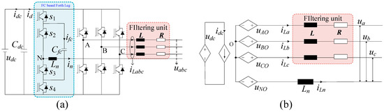
Figure 1.
(a). Topology of the proposed FCZS-3P4L converter, in which the three-level flying capacitor (FC) structure is introduced into the fourth zero-sequence leg. (b). Equivalent circuit model of the proposed FCZS-3P4L converter. (O is the ground point and also serves as the reference point for the controlled voltage source).
2.2. Mathematical Models
The FCZS leg has two pairs of switches (S1/S4 and S2/S3), in which upper and lower switches are typically driven by two sets of PWM carriers with a 180° phase shift, controlling the half-bridges S1/S4 and S2/S3, respectively, as shown in Figure 1a. Under identical duty cycle conditions, the flying capacitor voltage can be naturally maintained at equilibrium, ensuring Ufc = Udc/2. In this state, the flying capacitor can be equivalently analyzed as a half-bridge leg. Therefore, the equivalent circuit model of the FCZS-3P4L converter in the three-phase stationary coordinate system can be derived, as shown in Figure 1b.
Based on the equivalent circuit model, the output voltage of each bridge leg can be equivalently represented as a controlled voltage source as follows:
where Sa, Sb, Sc, and Sn represent the modulation waves of each bridge leg, respectively.
Based on the operating state of the bridge arm, the switching function Sx is defined as follows:
where Sx = 1 indicates that the upper switch is turned on and the lower switch is turned off. Similarly, when Sx = 0, it is the opposite situation.
Based on the KVL function, the loop voltage equations for each bridge leg are as follows:
Furthermore, the loop voltage equation of this system, as shown in Figure 1a, can be derived based on Kirchhoff’s Voltage Law (KVL):
where L = Ln denotes the filter inductance value; iLa, iLb, and iLc, respectively, denote the currents flowing through the inductors of phases A, B, and C; ua, ub, and uc refer to the AC network voltage; iLn represents the zero-sequence current; and idc indicates the current of the DC bus.
According to Kirchhoff’s Current Law (KCL) yields
Integrating Equations (3)–(5) yields the mathematical model of the three-phase four-leg converter as follows:
M is the inductance matrix, which can be expressed as follows:
Discretizing the above equations using the first-order forward Euler method yields the discrete mathematical model of the FCZS-3P4L converter under balanced flying capacitor voltage conditions as follows:
where ia(k + 1), ib(k + 1), ic(k + 1) are the predicted current values at the (k + 1)Ts; ia(k), ib(k), ic(k) are the predicted current values at the kTs; va(k), vb(k), vc(k) are the voltage vectors applied by the switching tube at the kTs; ua(k), ub(k), uc(k) are the measured voltage values at the kTs; and Ts is the sampling period.
Based on Equation (8), the current value at time (k + 1)Ts can be predicted with the sampled value at time kTs, which is the basis of the model predictive control. The key variables and parameters introduced in the above modeling process are summarized in Table 1 for clarity and reference.

Table 1.
Physical quantities involved in the modeling and analysis.
3. Mechanism of Double Harmonic Ripple in DC-Bus Voltage Under Unbalanced Conditions
In this section, the mechanism of double harmonic ripple in DC-bus voltage under three-phase power unbalanced conditions is presented. The details are as follows.
Assuming the AC side of the proposed FCZS-3P4L converter in SOP-FIDN systems is connected to the AC feeder source, in which the three-phase voltage is almost asymmetric, as shown in Figure 2. Assuming that three-phase voltage and current balance is achieved after compensating the distribution area, the asymmetric components in the output phase voltages become negligible compared to the positive-sequence component. Neglecting the negative-sequence and zero-sequence components, the mathematical expressions for the three-phase output voltages are as follows:
where Urms and ω represent the root mean square (RMS) value and the fundamental angular frequency of the three-phase output voltages, respectively. Under conditions of unbalanced three-phase loads in the distribution area, the three-phase load currents contain positive-sequence, negative-sequence, and zero-sequence components, which can be expressed as follows:
where I+, I−, and I0 are the RMS values of the positive-sequence, negative-sequence, and zero-sequence components of the three-phase compensation currents, respectively, while θi+, θi−, and θi0 are the initial phase angles of these components.
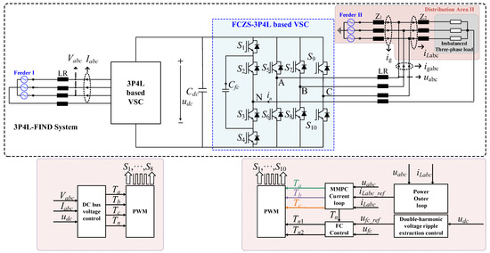
Figure 2.
Structure of the SOP-FIDN system based on 3P4L, where the conventional 3P4L voltage-source converter (VSC) is replaced by the proposed FCZS-3P4L converter. The conventional 3P4L VSC is primarily used to regulate the DC-link voltage, and its control strategy will not be discussed in detail in this paper. The proposed FCZS-3P4L converter is employed to balance the three-phase load currents in Area II and buffer the second-order harmonic voltage ripple on the DC side.
To simplify analysis and calculation, neglecting power losses of the converter, the instantaneous power on the AC load side of the 3P4L converter can be expressed as follows:
where Ps is the instantaneous power on the AC side, is the DC component, and is the pulsating component of the instantaneous power. Substituting Equations (9) and (10) into Equation (11), the specific expressions of each power can be expressed as follows:
Based on the law of power conservation, the DC-side current is given by Equation (13):
Therefore, the inverter DC-bus current idc can be decomposed into a DC component and a second-order harmonic AC component . In a conventional 3P4L converter, this second-order harmonic component will directly transfer to the DC voltage source, causing the double harmonic ripple and adversely affecting the stable operation of the voltage source or DC converter.
Assuming that the second-order harmonic pulsating power is entirely absorbed by the decoupling capacitor Cbuffer (the method of paralleling a large capacitor on the DC bus), the voltage across the decoupling capacitor consists of a DC component and a second-order harmonic pulsating component, expressed as follows:
where Uc,buffer is the voltage across the decoupling capacitor, Uc,dc is the DC source voltage, m is the ratio of the voltage ripple amplitude to the DC source voltage, and θ is the initial phase angle of the pulsating voltage. Therefore, the current flowing through the decoupling capacitor can be expressed as follows:
The second-order harmonic pulsating power buffered by the decoupling capacitor is then as follows:
To achieve power decoupling, the amplitude in Equation (16) should be equal to that of the second-order harmonic pulsating power on the load side in Equation (12), but with the opposite direction:
From Equation (17), the required DC-side capacitance can be calculated as follows:
Using the simulation and experimental parameters from this paper, the calculated value is Cbuffer = 2.738 mF.
Figure 3 illustrates the relationship between the DC-link voltage ripple (ΔU) and the DC-side capacitance Cbuffer under the operating conditions specified in this study. The overall trend demonstrates that as Cbuffer increases, the voltage ripple ΔU decreases significantly, exhibiting a non-linear attenuation behavior. The curve exhibits three typical operating points. Point A (29 V, 1.1 mF) indicates that the conventional method of relying solely on the DC bus capacitor to buffer second-order harmonic can result in significant DC voltage ripple under limited capacitance conditions. To achieve the same performance target as proposed in this work, a capacitance of Cbuffer = 1.5 mF (point B) is required. Point C (ΔU = 5%, Cbuffer = 0.82 mF) shows that, under the limiting condition of a 5% voltage ripple constraint, the required capacitance is 0.82 mF.
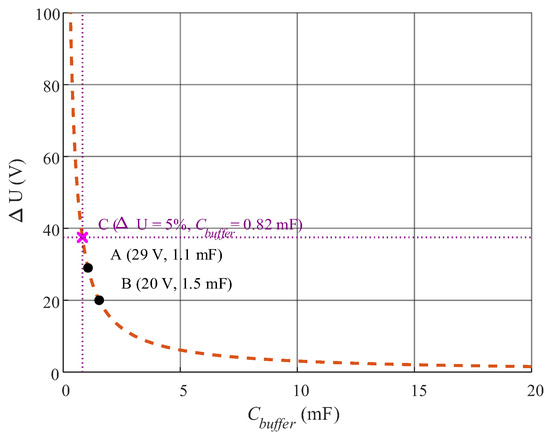
Figure 3.
Relationship between DC-bus voltage ripple (ΔU) and DC bus capacitance (Cbuffer).
4. Control Strategy of the Proposed FCZS-3P4L Converter
In the SOP-FIND system, the FCZS-3P4L converter has two main control goals. The first is used to achieve the split-phase power control to gain AC three-phase power imbalance compensation in Feeder II, and the second is used to dynamically regulate the flying capacitor voltage to suppress the second harmonic ripple in DC-bus voltage. The conventional control strategy typically involves multiple current control loops, where the coordinated tuning of control parameters across individual loops not only exerts a substantial influence on system stability but also introduces considerable complexity.
In this paper, a modulated model predictive control (MMPC)-based split-phase power and active power decoupling strategy for FCZS-3P4L converter is proposed. The overall control diagrams are presented in Figure 2, which have PQ-based phase-split reference current calculation and the double-harmonic extraction control outer loops to obtain the reference values for each phase current and flying capacitor voltage. Then, a modulated model predictive control (MMPC) loop is used to simultaneously realize AC split-phase current reference value tracking and independent flying capacitor voltage control, without the complex parameter coordination of multiple control loops in the conventional control structure.
4.1. PQ-Based Phase-Split Reference Current Calculation
The purpose of the PQ-based phase-split reference current calculation is to calculate the split-phase current reference values that can balance the power of each phase at the Feeder II power supply. The overall diagram is shown in Figure 4.
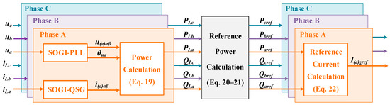
Figure 4.
Control diagram of PQ-based phase-split power loop for reference current calculation.
Firstly, the load power of each phase in distribution area II is calculated, which, according to the generalized instantaneous power theory for single-phase systems [16], can be expressed as follows:
where uxα, uxβ, ixα, and ixβ are the phase vectors for phases A, B, and C, respectively. The quadrature signals lagging by 90° are generated by a second-order generalized integrator-based quadrature signal generator (SOGI-QSG).
To achieve balanced three-phase voltages and currents in Feeder II after compensation, the unbalanced three-phase load must be compensated for such that the output three-phase power is balanced. Assuming the balanced phase-decoupled power output of the system is as follows:
where λ and γ are the active and reactive power coefficients, which represent the ratio of power supplied by Feeder II and the FIDN DC line.
Secondly, the reference value of each phase power can be collated as follows:
where Pxref represents the output power reference for phase x (A, B, C).
Finally, the reference values for each phase current can be obtained based on the instantaneous power theory, which can be expressed as follows:
where x = a, b, c, ux_rms represents the RMS voltage, Ix_peak is the amplitude of phase current, and θIx is the reference phase angle of the three-phase currents. Yx stands for the power transfer flow for each phase, Yx = 1 stands for power flows normally from DC to AC, and Yx = −1 stands for reverse flow occurring from AC to DC. This mechanism helps maintain system stability by preventing reverse power operation and provides clear directional guidance for current regulation.
4.2. Double-Harmonic Voltage Ripple Extraction Control
The purpose of double-harmonic voltage ripple extraction control is to calculate the flying capacitor reference value that can suppress double-harmonic voltage ripple in DC bus side.
The overall diagram of the double-harmonic voltage ripple extraction control is shown in Figure 5, in which a band-pass filter (BPF) is used to extract the second-order harmonic ripple component on the DC side, and then a quasi-resonant (QR) controller is employed to generate the flying capacitor voltage reference signals that can suppress double-harmonic voltage ripple in DC-bus side.
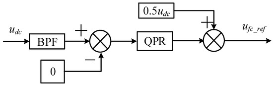
Figure 5.
Control block diagram of second-order harmonic pulsating voltage extraction.
4.3. MMPC-Based Inner Loop
After obtaining the reference value for each phase current and flying capacitor voltage, a MMPC-based inner loop is proposed to simultaneously realize AC split-phase current reference value tracking and independent flying capacitor voltage control, which consists of the phase current tracking MMPC and flying capacitor tracking MMPC parts. The implementation steps of the MMPC control loop are illustrated in Figure 6. The details are as follows.
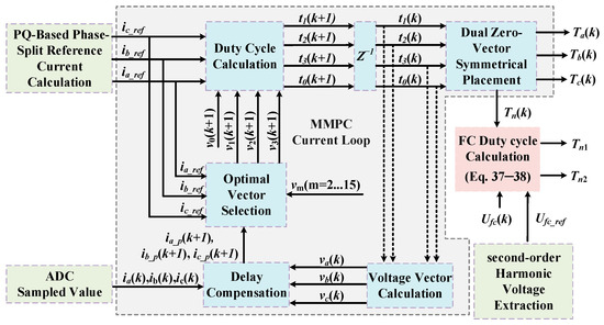
Figure 6.
Flowchart of the inner loop control based on MMPC.
4.3.1. MMPC Current Inner Loop
The MMPC current inner loop operates by evaluating a predefined cost function to select the optimal switching state, which reduces system parameter design complexity and enables theoretically optimal control.
Firstly, due to the inherent one-step delay in the system, to reduce the output current ripple of the converter, it is necessary to perform a two-step forward prediction based on the electrical quantities at time kTs as the initial condition [17]. This yields the predicted current values at time (k + 2)Ts, and the optimal voltage vector is selected via the cost function. Based on the three active voltage vectors v1(k), v2(k), v3(k) and the zero vector v0(k)—which are calculated at time (k − 1)Ts for application during the kTs cycle (i.e., from kTs to (k + 1)Ts)—the voltage vectors va(k), vb(k), vc(k) applied to phases A, B, and C during that same kTs cycle can be expressed as follows:
where v0a(k), v0b(k), v0c(k), v1a(k), v1b(k), v1c(k), v2a(k), v02b(k), v2c(k), v3a(k), v03b(k), and v3c(k) represent the a-phase, b-phase, and c-phase components of the voltage vectors v1(k), v2(k), v3(k) and v0(k), respectively. t1(k), t2(k), t3(k), and t0(k) denote the application times of v1(k), v2(k), v3(k), and the zero vector v0(k) during the kTs cycle.
Substituting Equation (23) into Equation (8), the predicted current values at the (k + 1)Ts instant are obtained as follows:
where ia_p(k + 1), ib_p(k + 1), ic_p(k + 1) represent the predicted current values of the inductor L at the (k + 1)Ts instant.
Secondly, the voltage values for phases A, B, and C are predicted after applying the 14 effective voltage vectors vm(m = 1…14) of the three-phase four-leg converter, yielding the predicted voltage values at the (k + 2)Ts period as follows:
where ua_p(k + 1), ub_p(k + 1), and uc_p(k + 1) are as follows:
Then, a cost function was calculated as follows:
The cost function is used to identify the three effective voltage vectors v1(k + 1), v2(k + 1), and v3(k + 1) with the lowest cost function values, which are selected as the non-zero voltage vectors for synthesizing the reference voltage vector.
After selecting the optimized three effective voltage vectors v1(k + 1), v2(k + 1), and v3(k + 1), the deadbeat control principle is applied to calculate the application times of the voltage vectors [18], i.e., the predicted values at the (k + 2)Ts period equal the reference values, which can be expressed as follows:
where δ0a(k + 1), δ0b(k + 1), δ0c(k + 1), δ1a(k + 1), δ1b(k + 1), δ1c(k + 1), δ2a(k + 1), δ2b(k + 1), δ2c(k + 1), δ3a(k + 1), δ3b(k + 1) and δ3c(k + 1) represent the current slopes under different voltage vectors in the (k + 1)Ts cycle, which can be expressed as follows:
The t1(k + 1), t2(k + 1), t3(k + 1), and t0(k + 1) denote the conducted times of v1(k + 1), v2(k + 1), v3(k + 1), and the zero vector v0(k + 1) during the (k + 1)Ts cycle, which satisfy the following equations as follows:
Combined with Equations (28)–(33), the conducted time of each vector can be expressed as follows:
where
If the sum of t1(k + 1), t2(k + 1), and t3(k + 1) exceeds one control period Ts, the application times of the voltage vectors are reallocated as follows:
Finally, after selecting the three voltage vectors for synthesizing the reference voltage vector and calculating their application times, the modulation signals Ta, Tb, Tc, and Tn for the conventional 3P4L converter are generated by arranging the switching vectors in a center-symmetric pattern with double zero vectors, as shown in Figure 7.
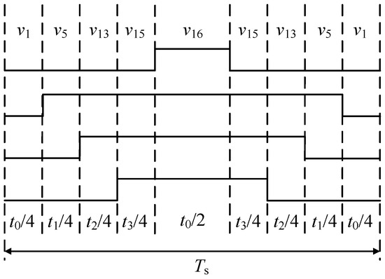
Figure 7.
Centrosymmetric arrangement of double-zero vectors (e.g., taking the effect of voltage vectors v1, v5, v13, v15, and v16 on the output).
4.3.2. MMPC Flying Capacitor Tracking Loop
Another object of the inner loop is to dynamically regulate the voltage of the flying capacitor to suppress double-harmonic voltage ripples on the DC-bus side. It is noted that the flying capacitor voltage can be naturally maintained under identical duty cycle conditions with a 180° phase shift PWM, i.e., [19], and the flying capacitor voltage can be regulated by the modification of the duty cycle FCZS leg.
To convenience analysis, the Tn is the basic duty cycle of FCZS leg, which can be obtained in MMPC current inner loop, and the modulated duty cycle for S1/S4 are defined as Tn1, and S2/S3 are defined as Tn2, and the relation between Tn1 and Tn2 can be expressed as follows:
Taking the fourth-leg flying capacitor structure as a specific example, the following section provides a detailed analysis of the underlying principle of actively controlling the flying capacitor voltage by adjusting the duty cycle increment.
Figure 8 shows the four switching states during reverse power transfer when ILn < 0. The flying capacitor charges if and only if the switching state is in Mode II (S1 = 0, S2 = 1). Conversely, it discharges if and only if the state is in Mode III (S1 = 1, S2 = 0).
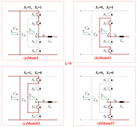
Figure 8.
The switching states during reverse power transfer in the fourth leg.
Figure 9a illustrates the waveform details of the fourth-leg flying capacitor when the duty cycle Tn < 0.5. Under this condition, Mode IV does not occur. Since the flying capacitor and the fourth-leg inductor are connected in series within the same branch during both Mode II and Mode III, the charging and discharging currents of the flying capacitor are numerically equal to the inductor current. When the switching state is in Mode III (S1 = 1, S2 = 0), the flying capacitor discharges. The amount of discharged charge corresponds to the area of the green region in the figure. When the switching state is in Mode II (S1 = 0, S2 = 1), the flying capacitor charges. The amount of charge corresponds to the area of the yellow region. Figure 9b shows the waveform details when the duty cycle Tn > 0.5. In this case, Mode I does not occur. Similarly, during Mode III (S1 = 1, S2 = 0), the flying capacitor discharges, with the discharged charge equal to the green area. During Mode II (S1 = 0, S2 = 1), the flying capacitor discharges, with the discharged charge equal to the green area. Therefore, by adjusting the duty cycle increment (represented by the red-shaded area in the figure), the difference between the charged and discharged quantities can be regulated, thereby enabling precise control of the flying capacitor voltage. Similarly, the four switching states during forward power transfer (when ILn > 0) can be derived.
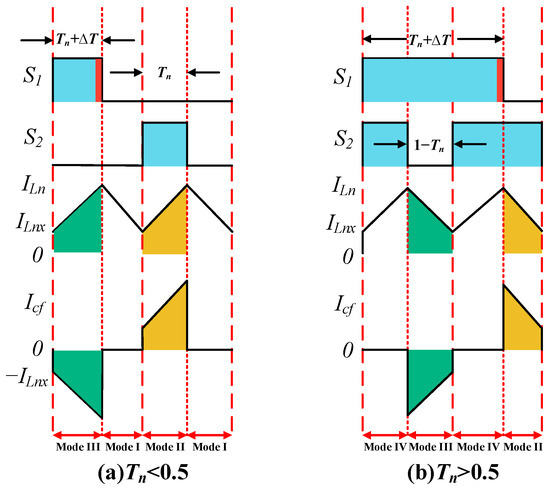
Figure 9.
Schematic diagram of flying capacitor charge/discharge drive signals based on compensation duty cycle.
Table 2 illustrates the relationship between the flying capacitor’s charge/discharge quantities and the duty cycle, as well as the compensation duty cycle. When ΔT < 0, Qcharge > Qdischarge; when ΔT > 0, Qcharge < Qdischarge. Therefore, introducing ΔT into the control system enables effective regulation of the flying capacitor voltage balance:
Table 2.
The relationship between the charge and duty cycle of the flyback capacitor is charging and discharging.
Regarding the new duty cycles Tn1 and Tn2 in Equation (37), since their calculated values may vary widely over a switching cycle, it is crucial to ensure Tn1, Tn2 ∈ [0, 1] to avoid saturation of the PWM signals. Therefore, if the sum of the new duty cycles exceeds 1 or falls below 0, the duty cycles must be clamped. The specific handling method is detailed in Table 3.
Table 3.
Duty cycle limitation.
5. Simulation and Experimental Validation
To verify the feasibility of the proposed FCZS-3P4L converter and the corresponding MMPC strategy, a MATLAB/Simulink-based (R2024b) simulation platform and a hardware-in-the-loop (HIL) experimental platform of the SOP-FIDN system have been built and tested. The system parameters are summarized in Table 4. The simulation results are shown in Figure 10, Figure 11 and Figure 12, and the experimental results are presented in Figure 13, Figure 14, Figure 15 and Figure 16.
Table 4.
Simulation and Experimental Parameters.
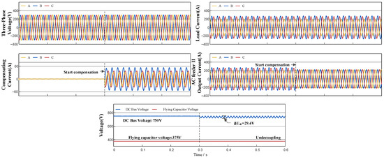
Figure 10.
Simulation results of the SOP-FIDN system using the proposed FCZS-3P4L converter with MMPC-based phase-split power compensation control, without DC second harmonic suppression control. Note that after enabling the compensation, Feeder II achieved balanced sinusoidal voltage and current outputs.
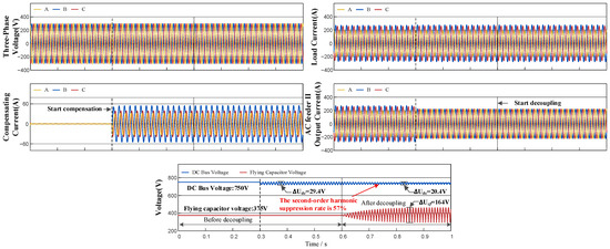
Figure 11.
Simulation results of the SOP-FIDN system with active flying capacitor voltage control buffering the second-order harmonic pulsation. Note that after enabling control, the second-order harmonic content decreased by 57%.
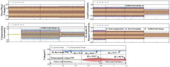
Figure 12.
Simulation results of the SOP-FIDN system under load disturbance conditions. As shown, the three-phase voltages and currents, along with the DC-bus voltage, all remain within acceptable limits during the disturbance process.
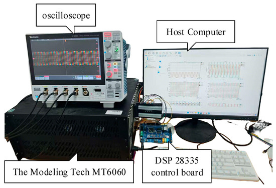
Figure 13.
Diagram of the experimental platform.
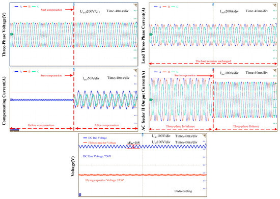
Figure 14.
Experimental result of the SOP-FIDN system using MMPC-based FCZS-3P4L phase-decoupled power compensation with dual-loop control. It is noteworthy that after enabling the MMPC-based phase-decoupled power compensation dual-loop control, Area II achieved balanced sinusoidal outputs for both voltage and current.
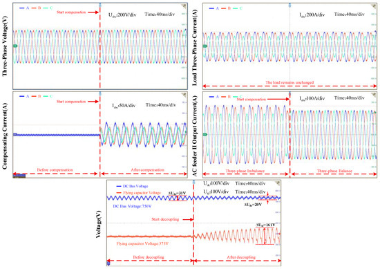
Figure 15.
Experimental result of the SOP-FIDN system with active flying capacitor voltage control buffering the second-order harmonic pulsation. It is noteworthy that after enabling active flying capacitor voltage control, the second-order harmonic content decreased by 57%.
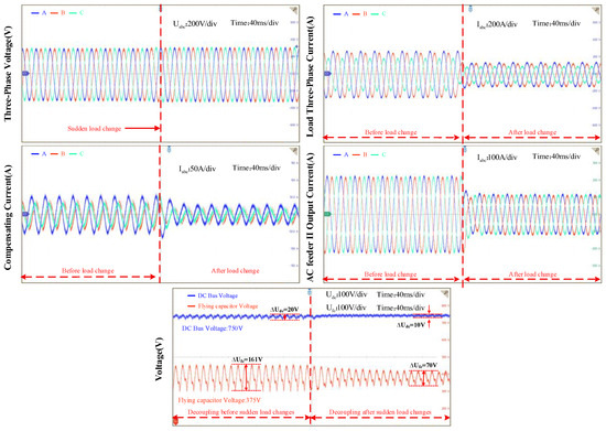
Figure 16.
Experimental results of the SOP-FIDN system under load disturbance conditions. As shown, the three-phase voltages and currents, along with the DC-bus voltage, all remain within acceptable limits during the disturbance process.
5.1. Simulation Results
To quantitatively characterize the asymmetry of current or voltage in a three-phase system, this paper adopts the degree of load imbalance as defined by IEEE standards. This metric is defined as the ratio of the negative-sequence component to the positive-sequence component in terms of RMS values and is typically expressed as a percentage as follows:
where λ denotes the degree of load imbalance (%), I− is the RMS value of the negative-sequence component, and I+ is the RMS value of the positive-sequence component.
Figure 10 shows the simulation results of the proposed FCZS-3P4L converter with MMPC-based phase-split power compensation control, without DC second harmonic suppression control. It can be seen that after enabling the proposed MMPC-based phase-split power compensation control, the voltages and currents of Feeder II become balanced, i.e., three-phase power is balanced. However, without enabling the DC second harmonic suppression control to control the flying capacitor, the DC-bus voltage exhibited a significant second-order harmonic ripple with an amplitude of 29.4 V and a DC voltage ripple factor of 3.92%, which severely threatens equipment operation. And the THD values of the load current for phases A, B, and C were 0.5%, 0.48%, and 0.48%, respectively.
Figure 11 shows the simulation results of the proposed FCZS-3P4L converter with MMPC-based phase-split power compensation and DC second harmonic suppression control. It can be seen that after enabling the DC second harmonic suppression control, the DC pulsating ripple has been significantly reduced, with an amplitude of 20.4 V and a DC voltage ripple factor of 2.72%, demonstrating the effectiveness of the proposed control strategy. Meanwhile, the THD values of the load current for phases A, B, and C were 0.49%, 0.51%, and 0.53%, respectively, indicating that the active flying capacitor voltage control did not affect the normal operation of the phase-spilt power compensation control.
To validate the dynamic performance of the proposed control strategy, tests under load disturbance conditions were conducted. The simulation results are presented in Figure 12. As shown, the three-phase voltages and currents, as well as the DC-bus voltage, all remain within acceptable limits throughout the disturbance transient. Meanwhile, the control system exhibits a fast dynamic response, with a settling time of approximately 12 ms, effectively demonstrating its ability to maintain voltage stability under sudden load variations.
5.2. Experimental Results
To validate the effectiveness of the control strategy in a practical system, a hardware-in-the-loop (HIL) experimental platform was built, as shown in Figure 13. The platform used a Modeling Tech MT6060 (sourced from ModelingTech Energy Technology Co., Ltd. Shanghai, China) as the hardware simulator and a DSP 28335 (sourced from Nanjing Yanxu Electrical Technology Co., Ltd., Nanjing, China) as the actual software controller. The system parameters were identical to those in the simulation, as listed in Table 3. Referring to the simulation case, hardware-in-the-loop (HIL) experiments were conducted for phase-decoupled power compensation control, second-order harmonic ripple suppression, and load disturbance rejection, respectively. The experimental waveforms are shown in Figure 14, Figure 15 and Figure 16.
This section employs hardware-in-the-loop (HIL) semi-physical simulation for validation. The core approach involves modeling of the plant (the FCZS-3P4L main power circuit) within a real-time simulator (MT6060), which forms a closed-loop system with the actual controller (DSP28335). This method enables rigorous verification of the real-time performance and effectiveness of the control algorithm while avoiding the high cost and risk associated with full-scale hardware prototype development.
The experimental waveforms for MMPC-based phase-decoupled power compensation control are shown in Figure 14. It can be seen that before the proposed MMPC-based phase-split power compensation control is enabled, the three-phase voltages and currents are severely unbalanced, with a current imbalance degree as high as 19.94%. After enabling the proposed MMPC-based phase-split power compensation control, the current imbalance in Feeder II was significantly reduced from 19.94% to 0.37%, while the three-phase voltages are also balanced.
Figure 15 shows the experimental waveforms for second-order harmonic pulsation suppression under active flying capacitor voltage control. It can be observed that, after enabling the DC second-harmonic suppression control, the amplitude of the DC pulsation is reduced from 31 V to 20 V. The ripple ratio of the DC-bus voltage is decreased from 4.13% to 2.67%. These results verify the effectiveness of the proposed buffering scheme for second-harmonic power pulsation.
Figure 16 presents the experimental waveforms under load disturbance conditions. As shown, he three-phase system voltages and currents remain balanced throughout the transient, and the DC bus voltage fluctuation is consistently confined within the acceptable range. Moreover, the flying capacitor voltage accurately tracks the second-harmonic voltage variation on the DC side in real time, thereby effectively suppressing the second-harmonic pulsation. These results fully validate that the proposed MMPC-based control strategy exhibits strong robustness and fast dynamic response even under dynamic load disturbances.
It should be noted that this HIL experiment does not encompass physical effects such as actual power device switching losses, parasitic parameters, and thermal dissipation. Consequently, its performance regarding efficiency evaluation and under extreme thermal stress still requires final validation through future full-scale prototype experiments. Nevertheless, for the verification of control logic, dynamic response, and key performance indicators (such as ripple suppression and balancing speed), this HIL platform provides sufficient and reliable evidence.
6. Conclusions
To address the issues of second-order harmonic fluctuations caused by mitigating three-phase imbalance and the complex control loops of conventional 3P4L converters in flexible interconnected power distribution areas, a multi-branch three-phase four-leg (FCZS-3P4L) converter and its control strategy are proposed. By replacing the fourth leg of the conventional 3P4L converter with a three-level flying capacitor structure, coordinated buffering of AC unbalanced power and DC second-order harmonic pulsation is achieved without additional buffer capacitors or decoupling circuits. The working principle and generation mechanism of the second-order harmonic ripple on the DC side are detailed. Based on the FCZS-3P4L system, an MMPC-based FCZS-3P4L phase-decoupled power compensation dual-loop control strategy and an active flying capacitor voltage control strategy are proposed. Simulation models and an HIL experimental platform were established. The results demonstrate that the proposed FCZS-3P4L converter and control strategy can simultaneously buffer the second-order harmonic ripple on the DC side and three-phase imbalance on the AC side, achieving balanced three-phase voltage and current outputs and reducing the amplitude of the second harmonic by 57%.
Author Contributions
Writing—original draft preparation: Y.M.; writing—review and editing: C.Z.; methodology and software: X.Y. and W.X.; data curation: Z.L. and H.Z.; supervision: Y.X. and Z.T. All authors have read and agreed to the published version of the manuscript.
Funding
This work was supported in part by the National Natural Science Foundation of China under Grant 62461008, in part by Guizhou Provincial Basic Research General Program (qiankehejichu-zk [2025]mianshang598), in part by the Youth Talent Growth Project of Guizhou Provincial Department of Education (Qianjiaoji [2024]21), and in part by Guizhou Province Science and Technology Support Plan (Qiankehe Support [2023] General 292).
Data Availability Statement
The original contributions presented in the study are included in the article; further inquiries can be directed to the corresponding author.
Conflicts of Interest
Authors Yutao Xu and Zhukui Tan were employed by the company Electric Power Research Institute of Guizhou Power Grid Co. The remaining authors declare that the research was conducted in the absence of any commercial or financial relationships that could be construed as a potential conflict of interest.
References
- Yang, M.; Zhai, H.; Ma, J.; Wei, S.; Wang, M.; Dong, Q. Dynamic Reconfiguration of Three-Phase Unbalanced Distribution Networks Considering Unbalanced Operation Constraint of Distributed Generation. Proc. CSEE 2019, 39, 3486–3499. [Google Scholar] [CrossRef]
- Xie, R.; Du, F.; Cheng, X.; Zhou, Q.; Xu, F. Influence of three-phase imbalance and harmonic on line loss of three-phase four-wire low-voltage distribution network. Power Syst. Prot. Control 2020, 48, 22–30. [Google Scholar] [CrossRef]
- Chugh, T.; Singh, A. Reactive power compensation using D-STATCOM with fuzzy logic supervision. In Proceedings of the 2016 IEEE 1st International Conference on Power Electronics, Intelligent Control and Energy Systems (ICPEICES), Delhi, India, 4–6 July 2016; pp. 1–6. [Google Scholar] [CrossRef]
- Liu, B.; Meng, K.; Dong, Z.Y.; Wong, P.K.; Ting, T. Unbalance Mitigation via Phase-Switching Device and Static Var Compensator in Low-Voltage Distribution Network. IEEE Trans. Power Syst. 2020, 35, 4856–4869. [Google Scholar] [CrossRef]
- Liu, S.; Jin, R.; Qiu, H.; Cui, X.; Lin, Z.; Lian, Z.; Lin, Z.; Wen, F.; Ding, Y.; Wang, Q.; et al. Practical Method for Mitigating Three-Phase Unbalance Based on Data-Driven User Phase Identification. IEEE Trans. Power Syst. 2020, 35, 1653–1656. [Google Scholar] [CrossRef]
- Deng, H.; Li, G.; Zhou, X.; Li, H.; Wang, H. The controltechnology of three-phase unbalance load in low voltage distributionnetworks based on coordinated controlled SVGs. Trans. China Electrotech. Soc. 2017, 32, 75–83. [Google Scholar] [CrossRef]
- Li, J.; Wang, G.; Zhang, M.; Fan, J.; Liu, S.; Lin, Z. Siting andsizing planning of automatic commutation device for three-phaseunbalance mitigation in distribution station area. Autom. Electr. Power Syst. 2022, 46, 62–69. [Google Scholar] [CrossRef]
- Tianlin, L.; Qi, G.; Xin, W. A Comprehensive Control Strategy for Three Phase Unbalance and Light and HeavyLoad in Flexible Interconnected Distribution Stations Based on F-SOP. Power Syst. Technol. 2024, 48, 4358–4367. [Google Scholar] [CrossRef]
- Yang, P.; Ming, W.; Liang, J.; Wu, J.; Liu, W. Reduction of DC-Link Ripples for SiC-Based Three-Phase Four-Wire Inverters with Unbalanced Loads. In Proceedings of the 2019 IEEE Energy Conversion Congress and Exposition (ECCE), Baltimore, MD, USA, 29 September–3 October 2019; pp. 2819–2835. [Google Scholar] [CrossRef]
- Jung, S.; Bae, Y.; Choi, S.; Kim, H. A Low Cost Utility Interactive Inverter for Residential Fuel Cell Generation. IEEE Trans. Power Electron. 2007, 22, 2293–2298. [Google Scholar] [CrossRef]
- Serban, I. Power Decoupling Method for Single-Phase H-Bridge Inverters with No Additional Power Electronics. IEEE Trans. Ind. Electron. 2015, 62, 4805–4813. [Google Scholar] [CrossRef]
- Zhou, J.; Lu, Z.; Xiong, W.; Yuan, X.; Ban, G.; Zhang, C.; Xu, Y.; Cai, Y.; Zheng, H. Two-terminal three-phase unbalance control strategy of flexible interconnected station area considering DC double frequency suppression. Electr. Power Autom. Equip. 2025, 45, 148–155. [Google Scholar] [CrossRef]
- Liu, Y.; Zhang, W.; Sun, Y.; Su, M.; Xu, G.; Dan, H. Review and Comparison of Control Strategies in Active Power Decoupling. IEEE Trans. Power Electron. 2021, 36, 14436–14455. [Google Scholar] [CrossRef]
- Ma, H.; Ye, H.; Gong, C. Control strategy of three-phase four-leg inverter using an auxiliary triangle waveform. Electr. Mach. Control 2016, 20, 14–21. [Google Scholar] [CrossRef]
- Zou, C.; Liu, B. Influence of Delay on System Stability and its Optimization in Grid-connected Inverters. Proc. CSEE 2015, 35, 411–417. [Google Scholar] [CrossRef]
- Mulla, A.M.; Rajagopalan, C.; Chowdhury, A. Hardware implementation of series hybrid active power filter using a novel control strategy based on generalised instantaneous power theory. IET Power Electron. 2013, 6, 592–600. [Google Scholar] [CrossRef]
- Zhang, Y.; Gao, S. Predictive current control for permanent magnet synchronous motor with delay compensation. J. Electr. Eng. 2016, 11, 13–20. [Google Scholar]
- Neves, F.A.S.; de Souza, H.E.P.; Cavalcanti, M.C.; Bradaschia, F.; Bueno, E.J. Digital Filters for Fast Harmonic Sequence Component Separation of Unbalanced and Distorted Three-Phase Signals. IEEE Trans. Ind. Electron. 2012, 59, 3847–3859. [Google Scholar] [CrossRef]
- Meynard, T.A.; Fadel, M.; Aouda, N. Modeling of multilevel converters. IEEE Trans. Ind. Electron. 1997, 44, 356–364. [Google Scholar] [CrossRef]


Disclaimer/Publisher’s Note: The statements, opinions and data contained in all publications are solely those of the individual author(s) and contributor(s) and not of MDPI and/or the editor(s). MDPI and/or the editor(s) disclaim responsibility for any injury to people or property resulting from any ideas, methods, instructions or products referred to in the content. |
© 2026 by the authors. Licensee MDPI, Basel, Switzerland. This article is an open access article distributed under the terms and conditions of the Creative Commons Attribution (CC BY) license.