1. Introduction
An AC contactor is a switch control electrical appliance which is widely applied in low-voltage power distribution systems. Due to frequent operations on the AC contactor in the power distribution system, the reliability of AC contactor control is related to the safety operation for power systems [
1]. The main factor which restricts the service life of the contactor is the electric arc caused by contact bounce, which brings about erosion [
2,
3]. It is also the bottleneck for the development of AC contactors. Therefore, there is an urgent need to conduct theoretical analysis on the switch-on, holding, and switch-off period of AC contactors, and propose effective control methods to reduce and suppress contact bounce, which is of great significance for improving the electrical life and reliability of AC contactors [
4,
5].
At present, for the research into AC contactors, domestic and foreign scholars mainly focus on the fields including residual electrical life, dynamic characteristics, material properties, mechanical structure, intelligent control, circuit topology structure, fault diagnosis, etc. [
6,
7,
8]. However, there are few studies on contact bounce. During the switch-on process, it contact bounce occurs on the AC contactor. During the switch-off process, the AC contactor will experience contact erosion, which causes its electrical life to be much lower than its mechanical life. During the holding process, the AC contactor generates significant noise and energy consumption, meaning that it cannot meet the development requirements of energy conservation and environmental protection. Therefore, the performance of the AC contactor will directly affect whether the power equipment can operate normally. Sun et al. evaluated the electrical wear state of the AC contactor based on unsupervised clustering and heterogeneous ensemble learning methods, and demonstrated the effectiveness of this method in practical implementation through illustrative examples [
9]. In addition, Sun et al. also studied the failure mechanism of the AC contactor under vibration conditions through simulation modeling and experimental verification [
10]. Xing et al. proposed a method for predicting the remaining electrical life of AC contactors using a convolutional autoencoder-bidirectional gated recurrent unit-attention, and the results demonstrate that the model has better prediction accuracy than recurrent neural network, long short-term memory, GRU, and BiGRU models [
11]. Guo et al. analyzed the dynamic characteristics of the AC contactor from three aspects: current characteristics, time characteristics, and velocity characteristics under different closing phase angles by using the finite element analysis method [
12].
Zeng et al. developed a novel AC contactor suitable for low-voltage environments based on the unique properties of the magnetic shape memory alloy. The results indicated that the novel AC contactor can effectively avoid the occurrence of contact bounce during the closing process [
13]. Saengsuwan et al. proposed a new simulation method for an AC electromagnetic contactor based on an electromagnetic transient program. The performance and accuracy of the proposed method were verified through the comparison of finite element simulation and experiments [
14]. Liu et al. proposed a degradation prediction method for an AC contactor based on K-means clustering and a Bayes optimized bi-directional long-short term memory neural network. The results indicated that the proposed method can better complete the division and prediction of the degradation state for the contactor [
15].
Shu et al. designed a new type of permanent magnet contactor which uses forced breaking to overcome failure conditions. Durability experiments were conducted to verify the protective function of the proposed permanent magnet contactor [
16]. Zhang et al. proposed an adaptive actuator driver for AC contactors based on the mathematical equations between the coil impedance and excitation control parameters. The results indicated that the driver has a plug-and-play function which can reduce the power consumption of the AC contactor [
17]. He et al. recorded the typical contact voltage, contact current, and coil current waveforms of the contactor during ac-1 electrical endurance tests. The failure mechanisms of the three-phase AC contactor were revealed through the analysis of the experimental phenomena [
18].
Chen et al. designed a novel energy-saving AC contactor by using two-phase magnetic material. The experimental results showed that the proposed energy-saving AC contactor has good functionality [
19]. Qi et al. constructed a closed-loop control system for contact motion characteristics based on speed feedback. The results indicated that the contact speed of the AC contact is obviously reduced, which can achieve the purpose of suppressing contact bounce [
20]. Park et al. proposed two types of two-level excitation-current electromagnetic contactor drives, which can reduce the drive power by employing features that have different conditions depending on the operating state of the electromagnetic contactor [
21]. Yang et al. proposed an uninterrupted switching topology for AC contactors from mains supply to a backup power supply based on the reverse external voltage turn-off characteristic of the silicon-controlled rectifier. The results showed that the proposed topology and its control strategy are feasible [
22].
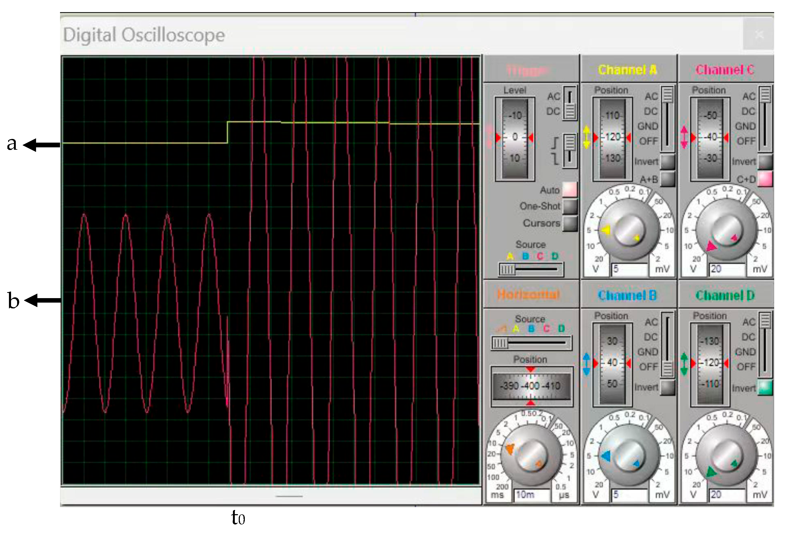
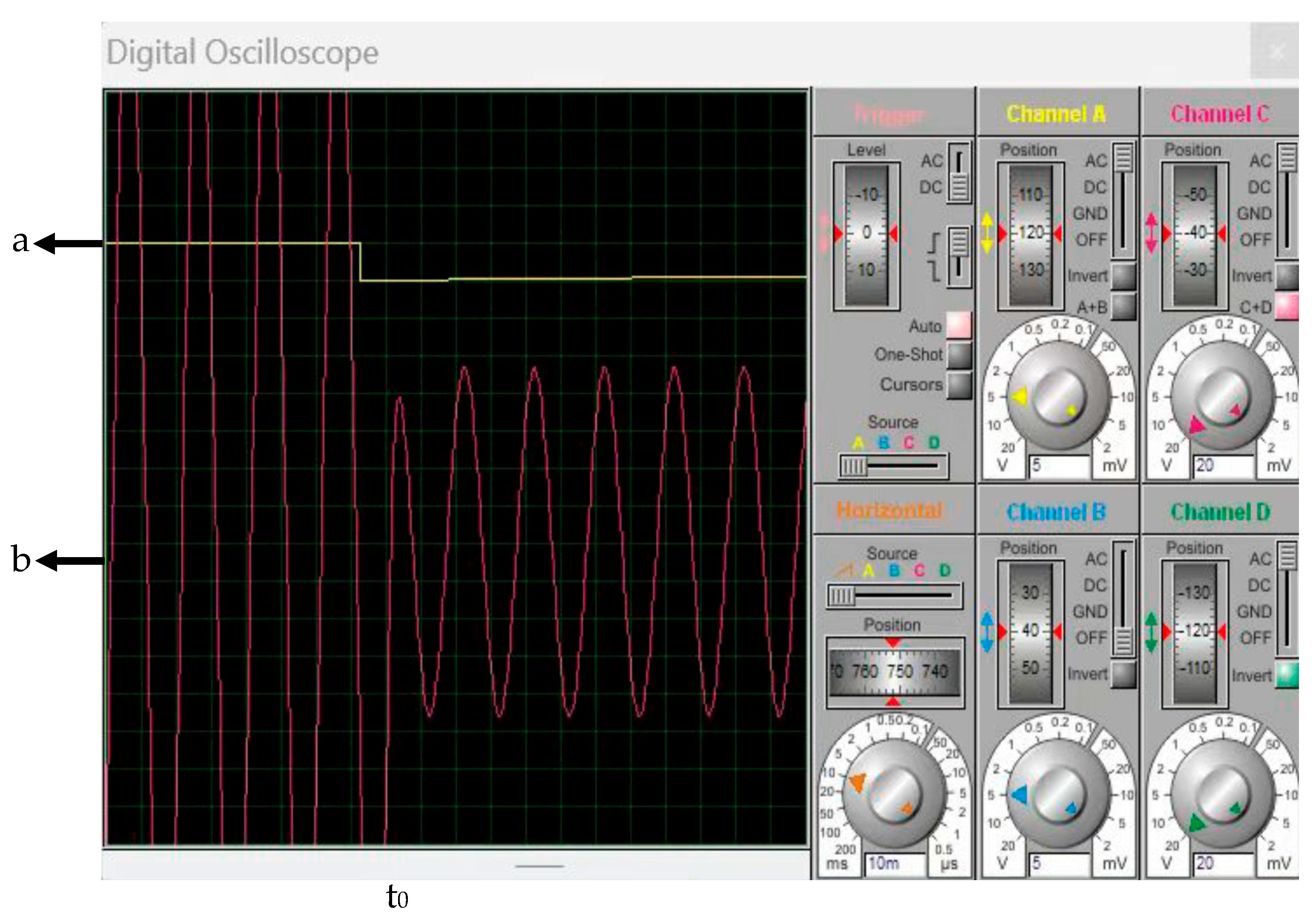
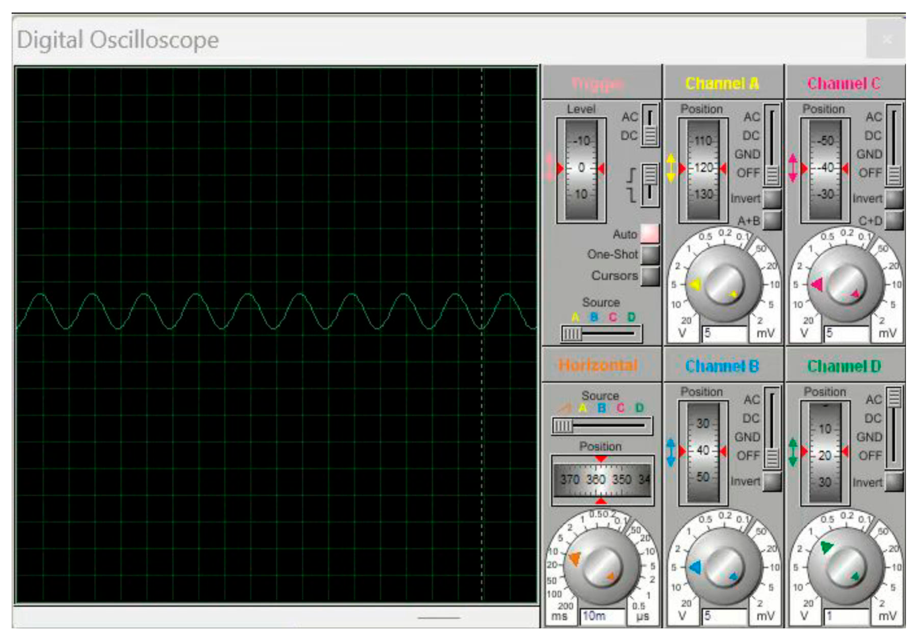
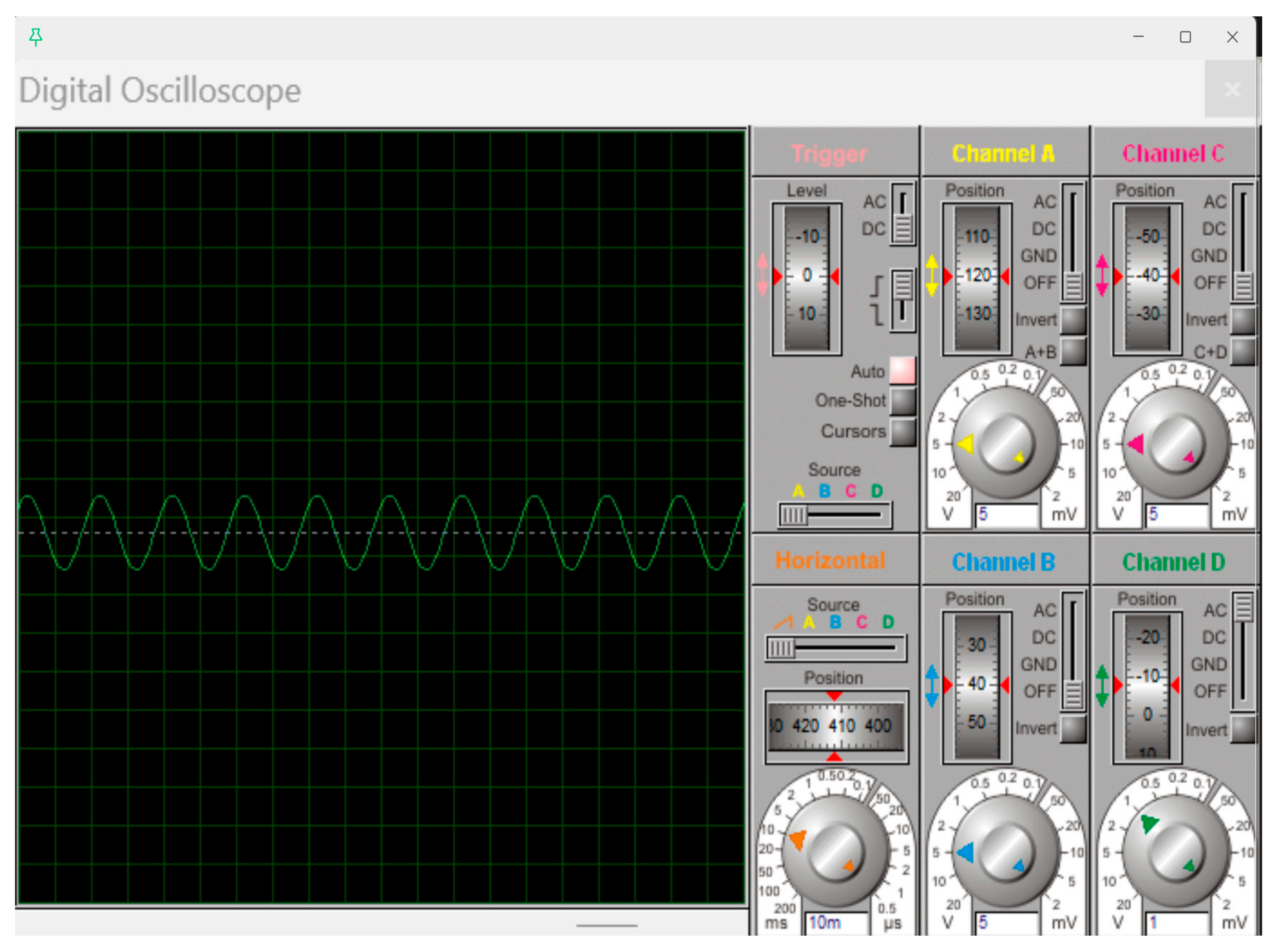
In this study, we mainly focused on solving the problem of contact erosion caused by contact bounce during the switch-on and switch-off period of an AC contactor. First, we conducted the theoretical analysis of an AC contactor during the switch-on, holding, and switch-off processes. Then, through theoretical analysis, we designed the driving circuits during the switch-on, holding, and switch-off processes. In addition, in order to detect the high voltage and large current signals in the main circuit, the three-phase voltage acquisition circuit and three-phase current acquisition circuit were designed. Finally, simulation testing and experimental verification were conducted, and the results indicated that the adopted scheme is feasible for reducing contact erosion.
2. Theoretical Analysis of the Switch-On, Holding and Switch-Off Process
2.1. Analysis of the Switch-On Process
The distance that the moving contact rebounds after the first collision can reflect the degree of contact bounce. Before and after the collision, the contact meets the law of conservation of energy. One part of the kinetic energy before the collision is consumed in the collision deformations of the contacts, another part is consumed in the contact spring, and the rest of the kinetic energy is consumed in the contact bounce. Therefore, according to the law of conservation of energy, Equation (1) is shown as follows:
where
is the mass of the moving contact,
represents the velocity of the moving contact before collision,
means the velocity of the moving contact after collision,
represents the energy consumed by the deformations of the moving and stationary contacts, and
stands for the energy consumed by the deformation of the spring.
In addition,
is defined as follows:
where
is the elasticity coefficient of the contact material and
represents the recovery coefficient of the contact material.
As the moving contact moves, the total distance that the spring is compressed can be defined as follows:
where
is the pre-compressed length of the reaction spring,
represents the compressive length of the spring after the moving contact rebounds, and
stands for the compressive length of the spring when the moving contact is under the attracting working condition.
Meanwhile, the elastic potential energy after the spring is compressed can be obtained by the following formula:
where
represents the elasticity coefficient of the spring and
stands for the total compressed length of the spring.
The reaction spring of an AC contactor has a pre-compressed distance, and the elastic potential energy of this part is not converted from the kinetic energy of the contact. Therefore, the elastic potential energy converted from the kinetic energy of the contact can be expressed by the following formula:
Assuming
, the velocity of the moving contact after collision can be obtained by the Formulas (1), (2) and (5), and it is defined as follows:
At the end of the first contact bounce (
),
, the maximum compressive length of the spring after the moving contact rebounds can be calculated by Formula (6), and it is defined below:
If the change in the rebound speed of the contact is proportional to time and
, then the average speed of rebound is approximately
and
is a constant which is greater than 2. Therefore, the time of the contact bounce is calculated as follows:
Therefore,
can be calculated by substituting Formula (8) into Formula (7), and it is shown as follows:
According to the analysis of Formula (9), it can be seen that there are many factors affecting the contact bounce. The initial pressure of the spring , the recovery coefficient of the contact material , the elasticity coefficient of the spring , and the mass of the moving contact all belong to the structural parameters, which have been determined during the design of the contactor and cannot easily be artificially changed. Therefore, the closing velocity of the contact is selected as the control factor to control the switch-on process. The closing velocity is affected by the electromagnetic attraction force. Therefore, using DC excitation instead of AC excitation is considered to eliminate or reduce the contact bounce.
In addition, mechanical vibration can also have an impact on contact bounce. It mainly accelerates contact degradation by intensifying mechanisms such as contact collision, arc energy, and physical wear. In order to reduce the contact erosion caused by mechanical vibration, the following methods can be adopted:
- (1)
Adjust the pressure of the contact spring to an appropriate range to avoid excessive or insufficient pressure;
- (2)
Optimize the electromagnetic system to ensure that the contact surface of the iron core is flat and clean, and check the integrity of the short-circuit ring;
- (3)
Install buffering devices (such as rubber pads or dampers) in the contact movement mechanism to absorb the collision energy, and maintain the contact surface regularly to repair eroded or deformed parts.
2.2. Analysis of the Holding Process
The current will flow through the coil when an AC contactor is powered on, then a closed magnetic flux loop will be formed along the air gap between the moving and stationary iron cores. Therefore, the electromagnetic attraction force generated can be defined as follows:
where
represents the numbers of windings of the coil,
is the permeability of vacuum,
means the cross-sectional area of the air gap between the moving and stationary iron cores,
stands for the total magnetic resistance of the magnetic flux, and
represents the excitation current flowing through the coil.
If the excitation power source is an AC power, Formula (10) can be defined as follows:
where
represents the peak value of the AC current,
is the peak value of electromagnetic attraction force during the AC excitation,
means the angular frequency of the AC current, and
stands for time.
According to Formula (11), the electromagnetic attraction force varies periodically between . Additionally, the electromagnetic attraction force is 0, especially when the current passes through the zero-crossing. Therefore, the AC contactor exists strong vibration during the holding process which resulted in severe noise. The air gap between the moving and stationary iron cores is very small when the switch-on process is completed, and a small excitation current will generate a large electromagnetic attraction force. As a consequence, a small excitation current can maintain the reliable holding of the AC contactor during the holding process. Hence, using low-voltage DC instead of high-voltage AC is considered for the holding process.
2.3. Analysis of the Switch-Off Process
The arc generated by the AC contactor will erode the contact during the switch-off process. Therefore, it is necessary to control the switch-off process to minimize the arc energy. The energy of the AC arc can be defined as follows:
where
represents the arc energy,
is the arc voltage,
means the arc current,
stands for the time,
represents the time when the arc is generated, and
means the time when the arc is extinguished.
Since
and
both change periodically with time,
is a positive value. In order to facilitate calculation,
is taken as a positive value and
is defined as an absolute value. Therefore,
and
can be assumed as the following formulas:
where
is the amplitude of the arc current,
represents the angular frequency of the main circuit power supply,
means the electric field intensity of the arc,
stands for the arc length, and
represents the voltage drop near the polar region of the electric arc.
Therefore, Formula (12) can be defined as follows:
Since the AC arc usually extinguishes when the current crosses zero, the upper limit of integral
is taken as
. Therefore, Formula (15) can be defined as follows:
According to the above Formula (16), it can be seen that the arc energy is proportional to the current flowing through the contact when the AC contactor breaks. The smaller the current, the smaller the arc energy, and the arc is not prone to occur. Therefore, this study takes the contact current as the control factor and uses the scheme of shunting control, thereby achieving the goal of few or even no arcs during the switch-off process.
3. Design of the Circuit Structure
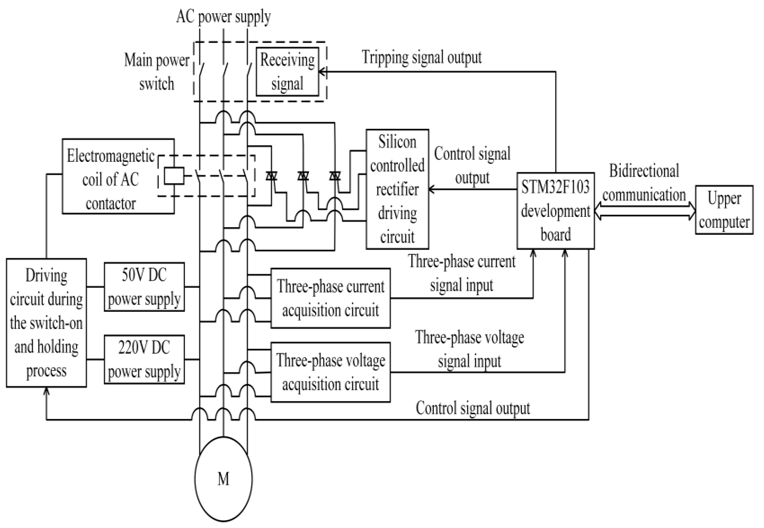
According to the above-mentioned problems during the working process of an AC contactor, the structure diagram of the hardware control system of an AC contactor is designed, and it is shown in
Figure 1.
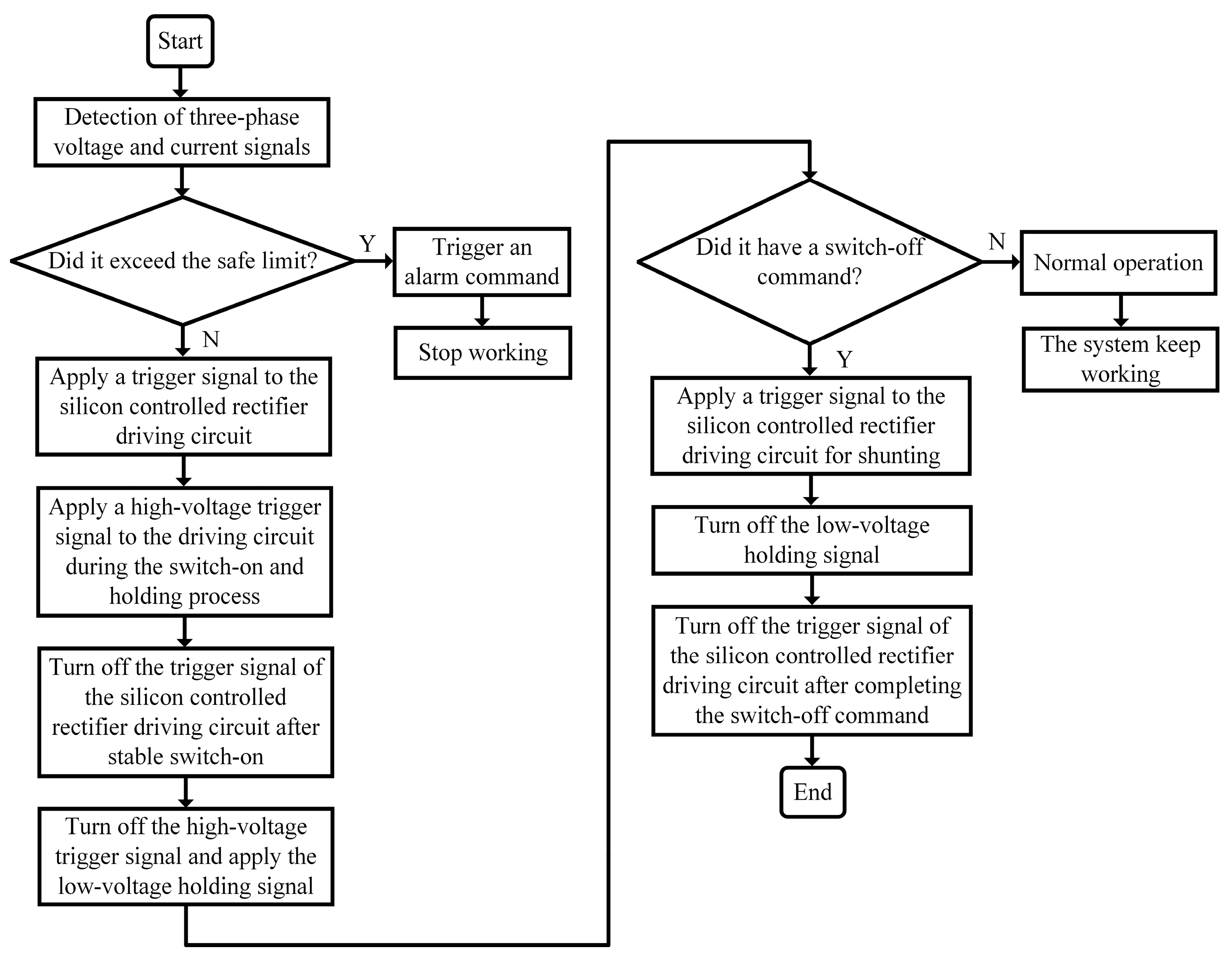
Figure 1 shows that the hardware control system is composed of the driving circuit during the switch-on and holding process, the silicon-controlled rectifier driving circuit during the switch-off process, three-phase voltage acquisition circuit, three-phase current acquisition circuit, and STM32F103 development board, among others. In addition, the working process of an AC contactor system is shown in
Figure 2.
3.1. Design of the Driving Circuit Structure During the Switch-On and Holding Process
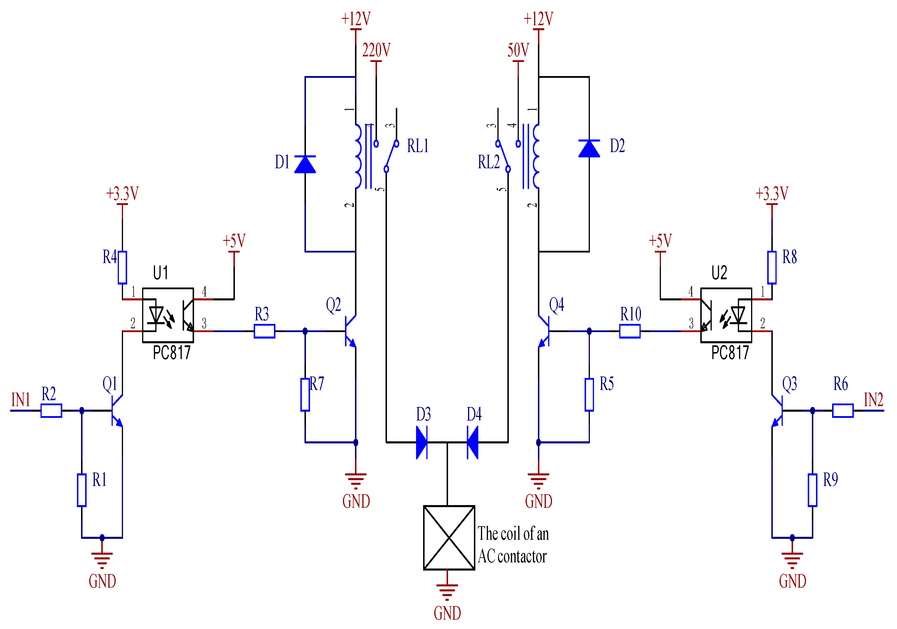
According to the above theoretical analysis, the driving circuit during the switch-on and holding process is designed, and it is shown in
Figure 3.
Figure 3 shows that the circuit is mainly composed of micro relays, photoelectric couplers, diodes, transistors, and resistors. Meanwhile, the circuit has five different DC voltage sources. The input pull-up control voltage of the photoelectric coupler is provided by the STM32F103 development board, and the other excitation voltages are provided by the DC power supply. The micro relay RL1 is used to control the opening and closing of the 220 V DC power supply by inputting the 12 V direct current, and RL2 is used to control the opening and closing of the 50 V DC power supply by inputting the 12 V direct current. The functions of diodes D1 and D2 are to protect the micro relays from generating reverse voltage when the circuit is disconnected, thereby protecting the micro relays from damage. D3 and D4 are two reverse parallel diodes with a reverse withstand voltage of up to 1000 V, which can withstand the high reverse voltage generated when the coil is powered off and protect micro relays. In addition, D3 and D4 can prevent short circuits between 220 V and 50 V DC power supplies and isolate the power sources, thereby ensuring the safety of the circuit.
Moreover, the circuit contains two photoelectric couplers PC817, which have two main functions in this circuit. Firstly, the light is used as the transmission medium to separate the strong and weak electricity of the circuit, which can ensure the safe and efficient connection between the strong and weak electricity circuits. Secondly, the collecting electrode pins of the photoelectric couplers are connected to the +5 V DC power supply to provide the base voltage for transistors Q2 and Q4, thereby controlling the opening and closing. The main functions of transistors Q1 and Q3 are to provide sufficient operating current for the cathode pins of the photoelectric couplers. In addition, the main functions of transistors Q2 and Q4 are to control the opening and closing of the +12 V DC voltage source at both ends of micro relays RL1 and RL2. The functions of the resistors R3, R7, R5, and R10 are to ensure that the base voltage is zero when the forward bias voltage is 0 mv, thereby preventing the transistors Q2 and Q4 from being disturbed by the external factors.
Furthermore, the transistor Q1, photoelectric coupler U1, and transistor Q2 conduct in sequence when the pin IN1 outputs a high-level signal. Then, the pin 2 of the micro relay RL1 is connected to the ground. Meanwhile, the +12 V DC voltage source makes the pins 4 and 5 of the micro relay RL1 conduct, and the +220 V DC voltage source is quickly loaded across the ends of the AC contactor coil. The signal from the pin IN1 is turned off while the pin IN2 outputs a high-level signal. Similarly, the +50 V DC voltage source is loaded across the ends of the AC contactor coil, and the driving circuit can achieve the purpose of low-voltage maintenance and energy conservation.
3.2. Design of the Silicon-Controlled Rectifier Driving Circuit Structure During the Switch-Off Process
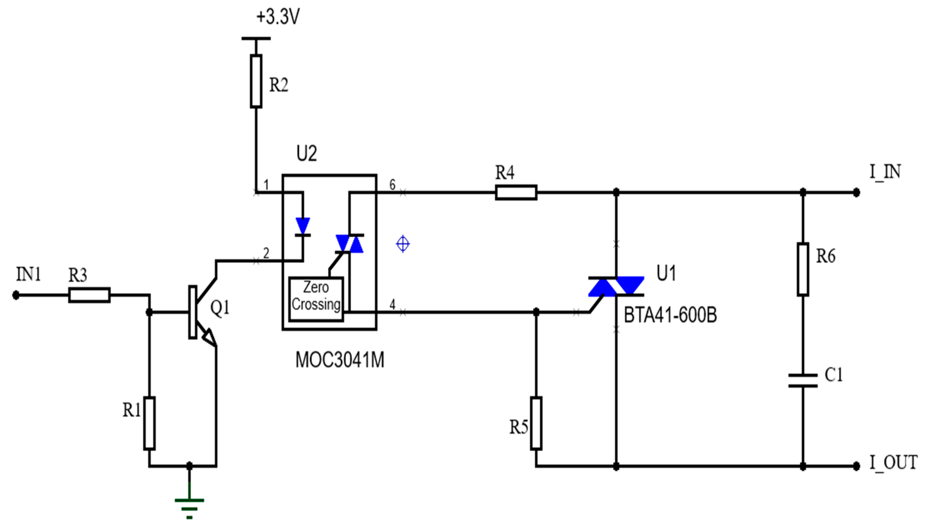
According to the above theoretical analysis, the driving circuit during the switch-off process is designed, and it is shown in
Figure 4.
Figure 4 shows that the circuit is mainly composed of silicon-controlled rectifier, photoelectric coupler, transistor, capacitance, and resistors. The silicon-controlled rectifier selected in this circuit is BTA41-600B. In order to prevent the silicon-controlled rectifier from misconducting when there is no gate trigger voltage, the driving circuit adopts the parallel resistance–capacitance circuit at both ends of the silicon-controlled rectifier, which is as shown in
Figure 4 with the capacitance C1 and the resistor R6.
In addition, the photoelectric coupler selected in this circuit is MOC3041M, and the input pull-up control voltage of the photoelectric coupler is provided by the STM32F103 development board. The transistor Q1 and photoelectric coupler U2 conduct in sequence when the pin IN1 outputs a high-level signal. Meanwhile, the gate of the silicon-controlled rectifier U1 connected to pin 4 of the photoelectric coupler U2 receives a trigger signal when the current flows between I_IN and I_OUT in
Figure 4; then, the anode and cathode of the silicon-controlled rectifier U1 can be turned on. Therefore, the silicon-controlled rectifier U1 can undertake the current when the AC contactor breaks, thereby achieving the goal of arc-free breaking and enhancing the breaking capacity. Furthermore, R4 is the trigger current-limiting resistor, and R5 is the gate resistor of silicon-controlled rectifier U1, which can prevent the false triggering and improve the anti-interference capability, thereby ensuring that the current flowing through the gate of silicon-controlled rectifier U1 is within the safe operating range.
3.3. Design of the Three-Phase Voltage Acquisition Circuit
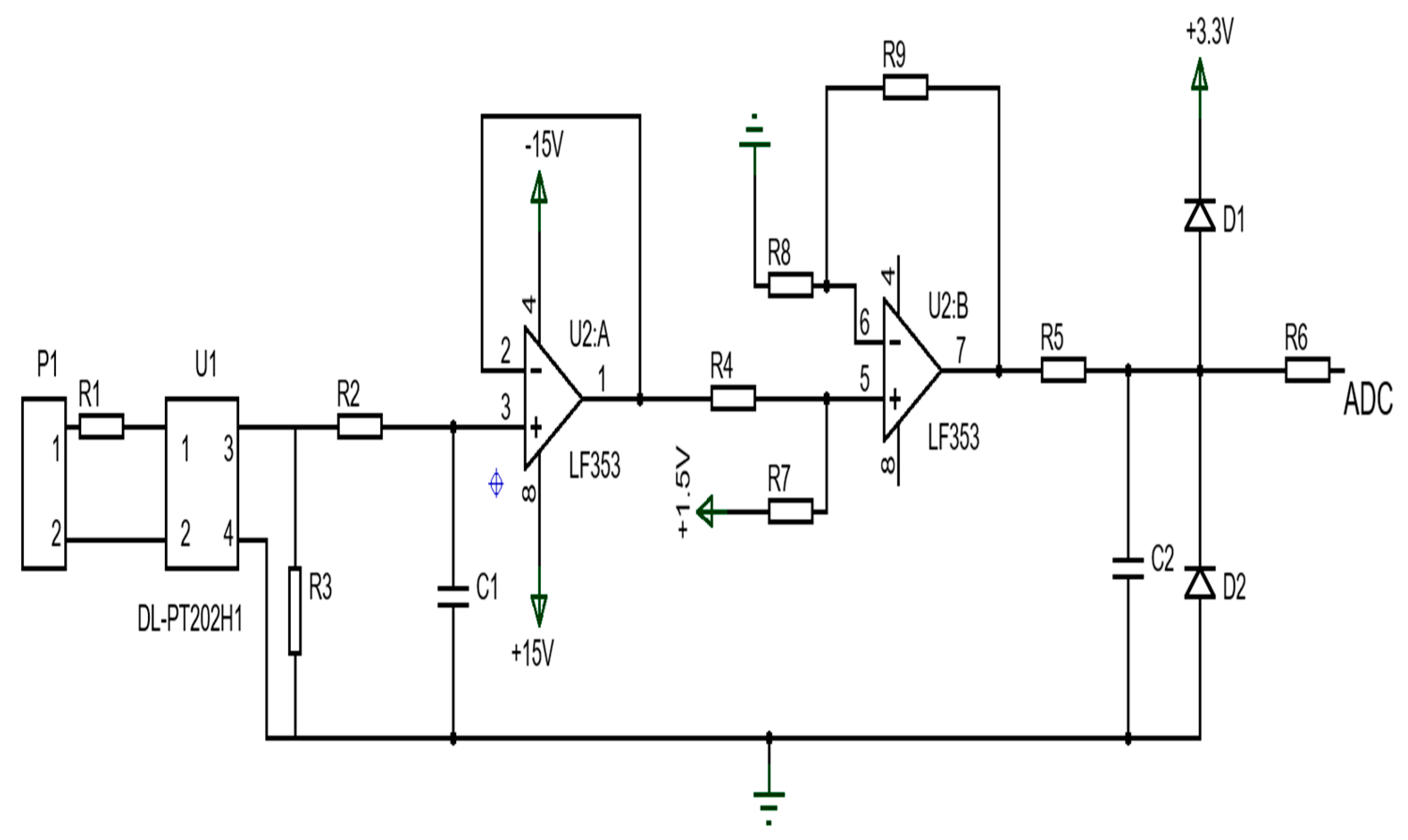
The purpose of the three-phase voltage acquisition circuit is to convert the high-voltage signal of the main circuit into a low-voltage signal that can be received by the STM32 controller. Moreover, all signals of the positive and negative half cycles for the AC voltage should be retained during the conversion process, and it can also suppress certain harmonic interference. The three-phase voltage acquisition circuit is shown in
Figure 5. The core components of the circuit include a voltage transformer and an operational amplifier. The design methods of the other two phases in this circuit are exactly the same. Therefore, the schematics of the voltage acquisition for the other two phases are not provided.
The voltage transformer selected in this circuit is DL-PT202H1, which is a current-type voltage transformer with four ports. The working parameters of DL-PT202H1 are shown in
Table 1.
The protection range of the voltage transformer is set between 0.7 and 1.5 times. If the effective value of the AC voltage is 220 V, the range of effective value for the input AC voltage is between 150 V and 330 V. The value of current-limiting resistor R1 at the input end of the voltage transformer is 110 kΩ. The input currents of the ports 1 and 2 for the voltage transformer range from −2.828 mA to +2.828 mA when the input AC voltage is 220 V.
Table 1 shows that the turns ratio of the voltage transformer is 1500:1500, and the output currents of the ports 3 and 4 also range from −2.828 mA to +2.828 mA. In
Figure 5, R3 is the sampling resistor, and the resistance value is 388Ω according to the calculation. Thus, the input voltage amplitude of pin 3 for the operational amplifier is 0.999 V. In
Figure 5, the resistor R2 and the capacitor C1 form an integrating circuit and constitute a low-pass filter which can filter out high-order harmonics and prevent the operational amplifier from oscillating. Meanwhile, the resistor R2 can also have the function of current limiting.
The operational amplifier selected in this circuit is LF353. In order to facilitate presentation in the circuit diagram, the operational amplifier LF353 is split into two parts which correspond to U2:A and U2:B in
Figure 5, respectively. Pins 4 and 8 are dual power inputs, for which the voltage ranges from −18 V to +18 V. Pin 4 is connected to the −15 V DC power supply and pin 8 is connected to the +15 V DC power supply. The output pin 1 of the operational amplifier U2:A is connected to the inverting input pin 2 with a single wire, and the operational amplifier is connected as a voltage follower to enhance the input impedance and increase the loading capacity of the sampling terminal. Meanwhile, it can also isolate the front and rear stage circuits, thereby eliminating their mutual influence. If the voltages of pins 1, 2, 3, 5, 6, and 7 are U1, U2, U3, U5, U6, and U7, respectively, according to the concept of virtual short circuit, the voltage range of pins 2 and 3 can be expressed by the following formula:
According to the principle of the voltage follower, the voltage range of pins 1 and 2 can be obtained by the following formula:
The input pin 5 of the operational amplifier U2:B is connected in parallel with two branches. One branch is connected to the output voltage U1 of the operational amplifier U2:A which ranges from −0.999 V to +0.999 V. The other branch is connected to the +1.5 V DC voltage source. Furthermore, the input voltage of the pin ADC of the STM32 development board must be greater than zero, and the output voltage of the operational amplifier U2:A is −0.999 V when the signal of the negative half cycle is collected. If the signal of the negative half cycle is not processed, the circuit board will not receive the corresponding signal. In order to reserve voltage signal of the negative half cycle, another voltage branch needs to be provided to convert the negative voltage signal into a positive voltage signal. Therefore, two branches are added to the input end of the operational amplifier U2:B. According to the concept of virtual open circuit, Formulas (19) and (20) are defined as follows:
According to the concept of the virtual short circuit, the input voltage of pins 5 and 6 can be obtained by the following formula:
In addition, the values of resistors R4, R7, R8, and R9 selected in this circuit are all 10 kΩ. Therefore, the output voltage of pin 7 can be obtained by Formulas (19)–(21), and it is defined as follows:
According to Formula (22), the input voltage U1 ranges from −0.999 V to +0.999 V. Therefore, the output voltage U7 ranges from 0.501 V to 2.499 V, thereby ensuring that the minimum voltage received by the STM32 development board is greater than 0 V and the maximum voltage is lower than +3.3 V.
In
Figure 5, the resistor R5 and the capacitor C2 constitute a low-pass filter which can eliminate the high-frequency noise. The function of the resistor R6 is to eliminate reflection. The diodes D1 and D2 selected in this circuit are 1N5822, which can form a clamping circuit. This clamping circuit can keep the output voltage range from 0 V to +3.3 V, thereby meeting the input range of the signals received by the STM32 development board. If the collected signal suddenly increases and the voltage received by the circuit board exceeds the threshold, the diodes D1 and D2 can quickly conduct and shunt to protect the STM32 development board.
3.4. Design of the Three-Phase Current Acquisition Circuit
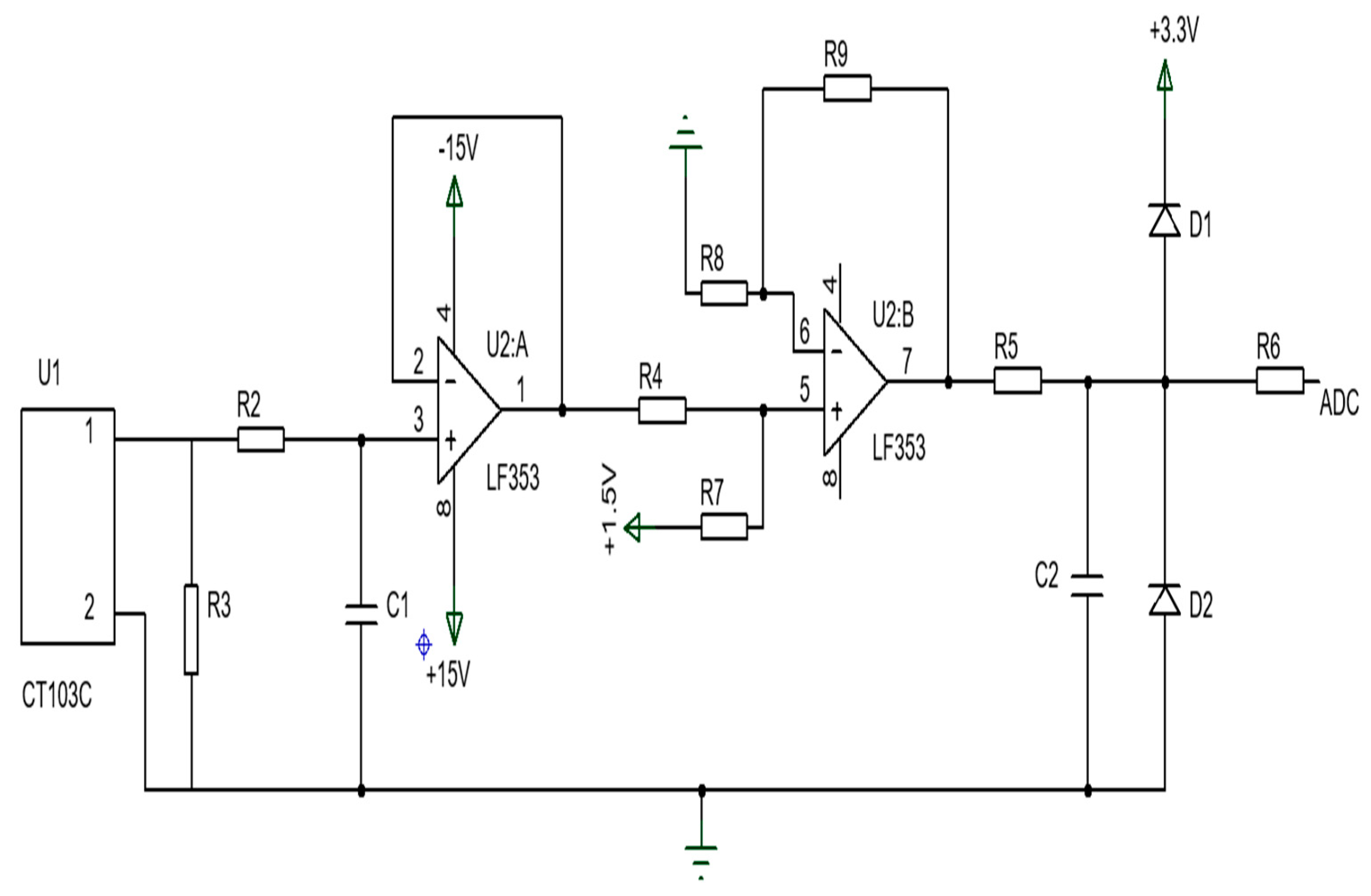
The function of the three-phase current acquisition circuit is to convert the high current signal of the main circuit into a low-voltage signal, which can be received by the STM32 development board. Therefore, the design of the current acquisition circuit is similar to that of the previous voltage acquisition circuit. The three-phase current acquisition circuit designed in this paper is shown in
Figure 6. The core components of the circuit include a current transformer and an operational amplifier. The current transformer selected in this circuit is CT103C, and the working parameters of CT103C are shown in
Table 2.
The protection range of the current transformer is also set between 0.7 and 1.5 times. If the effective value of the AC current is 5 A, the range of the effective value for the input AC current is between 3.5 A and 7.5 A. In
Figure 6, R3 is the sampling resistor and the resistance value is 213 Ω. Therefore, the input voltage amplitude of pin 3 for the operational amplifier is still 0.999 V. Moreover, the remaining circuit structures are completely consistent with the three-phase voltage acquisition circuit. Finally, the high current signal can be converted into a low-voltage signal that can be received by the STM32 development board.
5. Experimental Testing
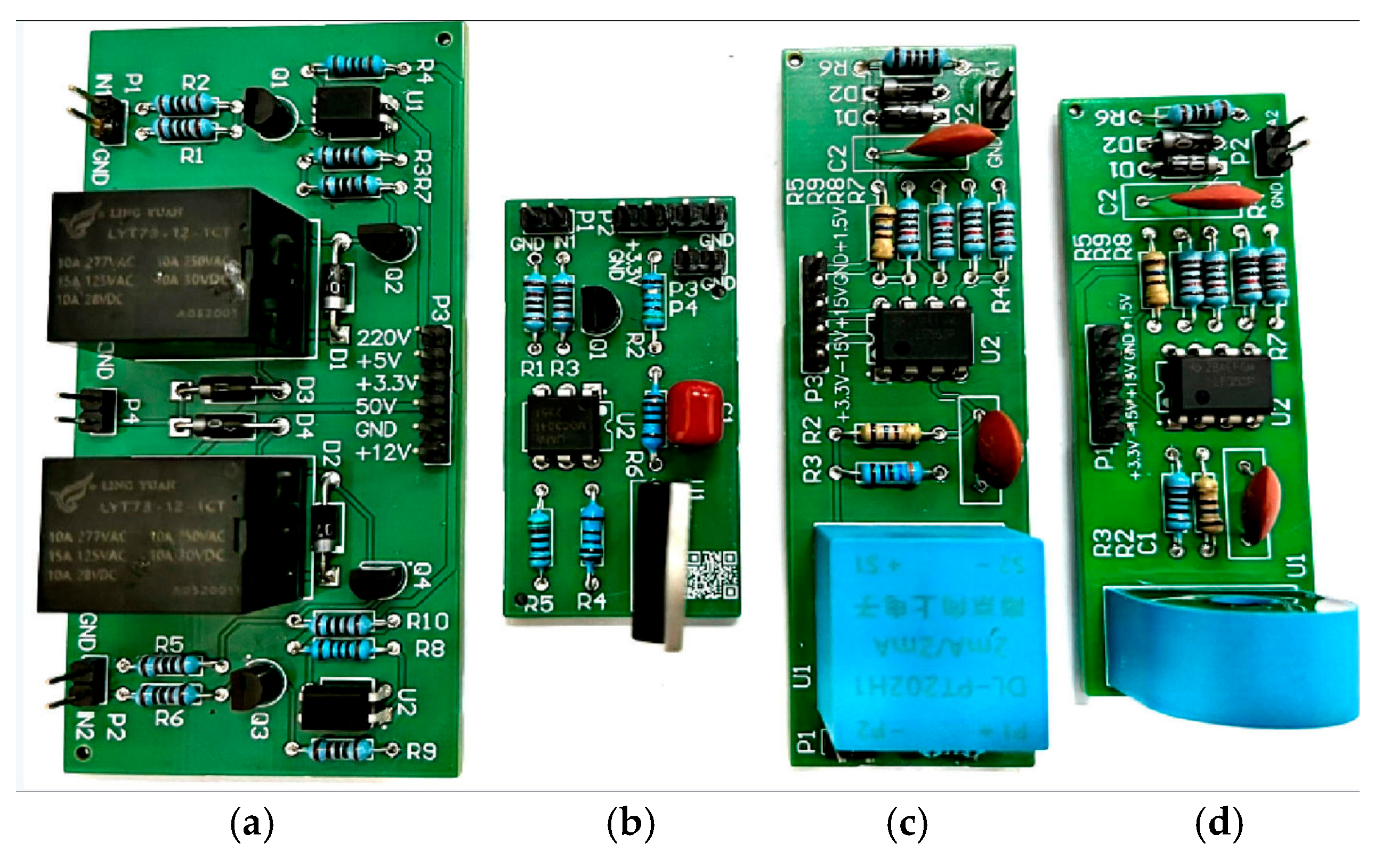
According to the above simulation testing analysis, the hardware circuit is designed, and it is shown in
Figure 13.
Figure 13a shows the driving circuit during the switch-on and holding process.
Figure 13b shows the silicon-controlled rectifier driving circuit during the switch-off process.
Figure 13c,d show the three-phase voltage acquisition circuit and three-phase current acquisition circuit, respectively.
In addition, in order to verify the correctness of the designed hardware circuit, the Delixi CJX2H-120 AC contactor was used for relevant experiments, and the expected designed circuit can be applied to industrial and residential distribution.
Table 3 shows the main technical parameters of the Delixi CJX2H-120 AC contactor.
In fact, different loads will change the phase relationship between voltage and current, power consumption, and the patterns of energy flow, thereby affecting the overall performance of the designed circuit. The loads mainly include resistive loads, inductive loads, and capacitive loads. Resistive loads have no impact on the stability of the designed circuit. Inductive loads can store the energy of magnetic field, which causes the current phase to lag behind the voltage phase and reduces the power factor. Meanwhile, it may cause voltage fluctuations and generate electric arcs. For the inductive loads, it is necessary to add a freewheel diode to the designed circuit to ensure a stable current path when the AC contactor is turned off. Capacitive loads can store the energy of the electric field and impede the voltage changes, thereby causing the current phase to lead the voltage phase. In addition, surge currents may occur under heavy loading. For the capacitive loads, it is necessary to adopt soft-starting technology to limit the inrush current at the moment of power-on by the cooperation of the current limiting resistor and NTC thermistor, thereby protecting the designed circuit from damage. During the experiment, a resistive load was used; therefore, the influence of the load on the designed circuit is not described in our paper.
5.1. Experimental Testing of the Driving Circuit During the Switch-On and Holding Process
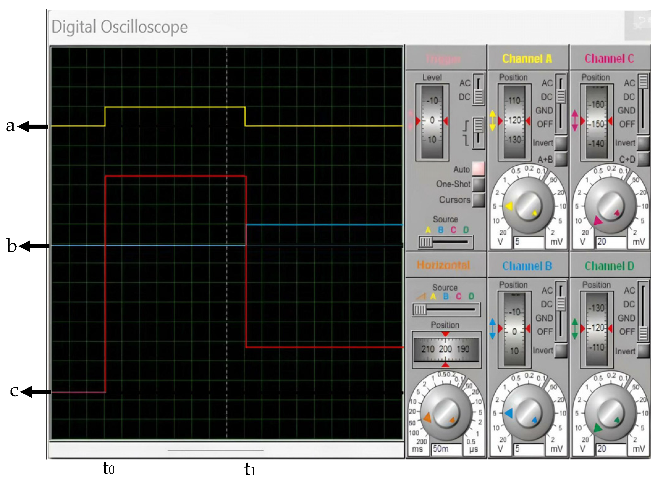
The digital oscilloscope SDS804X HD produced by Dingyang company was used for experimental testing. This oscilloscope has four channels and can simultaneously collect image data. In terms of the driving circuit during the switch-on and holding process, it is necessary to utilize two GPIO ports of the STM32 development board to output high and low levels to control the opening and closing of the micro relays RL1 and RL2.
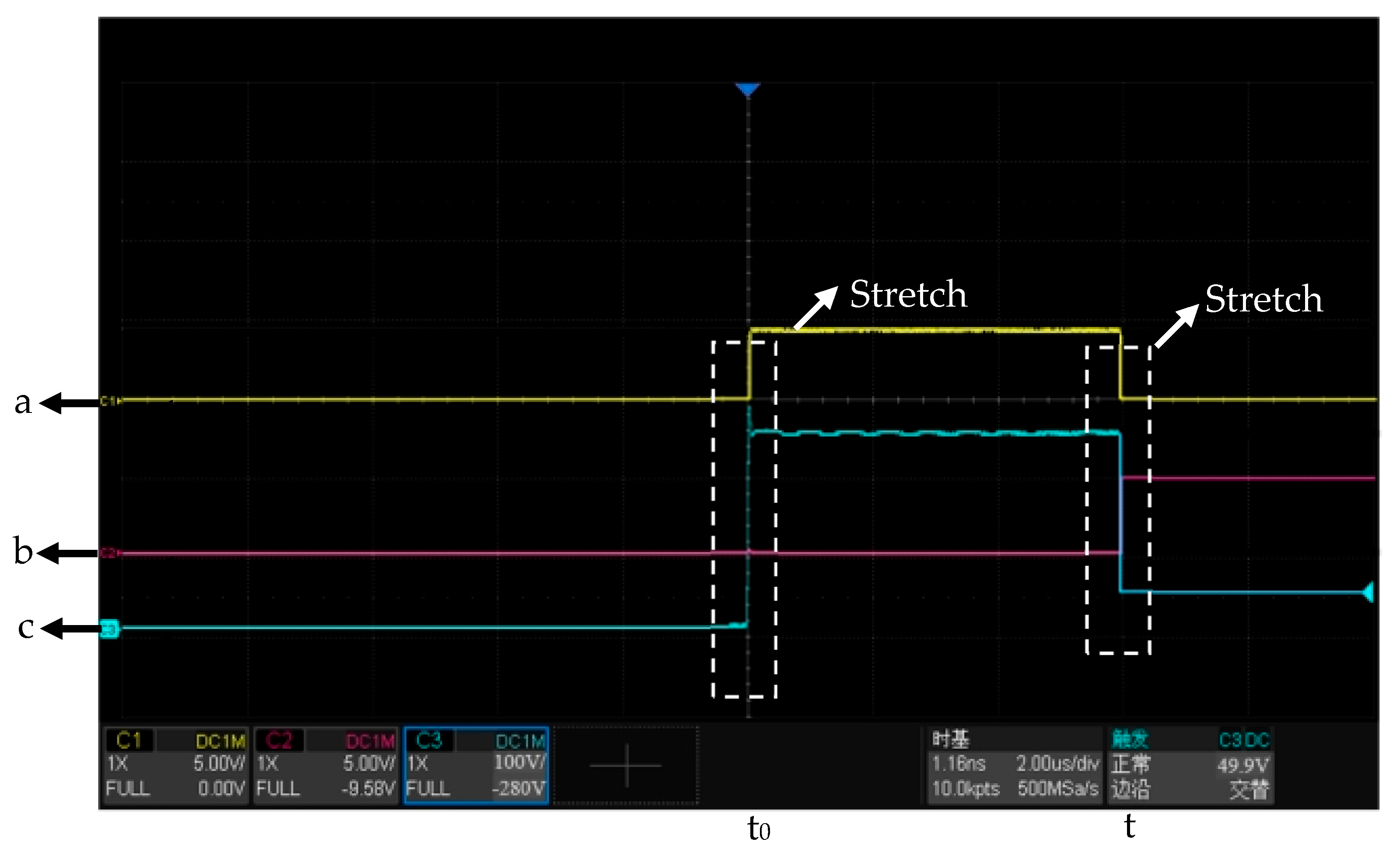
Figure 14 shows the oscillogram of the experimental testing for the 220 V–50 V high–low-voltage switching. As can be seen from
Figure 14, channels 1 and 2 measure the trigger signals of pins IN1 and pin IN2, respectively, and the voltage setting is at 5 V per division. Channel 3 measures the voltage signal at both ends of the coil, and the voltage setting is at 100 V per division. Furthermore, the time setting is at 2 μs per division.
In
Figure 14, the voltage at both ends of the coil increases from 0 V to 220 V when the trigger signal of pin IN1 rises from a low level to a high level at time t0. The trigger signal of pin IN1 decreases from a high level to a low level when the trigger signal of pin IN2 rises from a low level to a high level at time t1, then the voltage at both ends of the coil decreases from 220 V to 50 V.
The oscillogram at time t0 in
Figure 14 is stretched to obtain
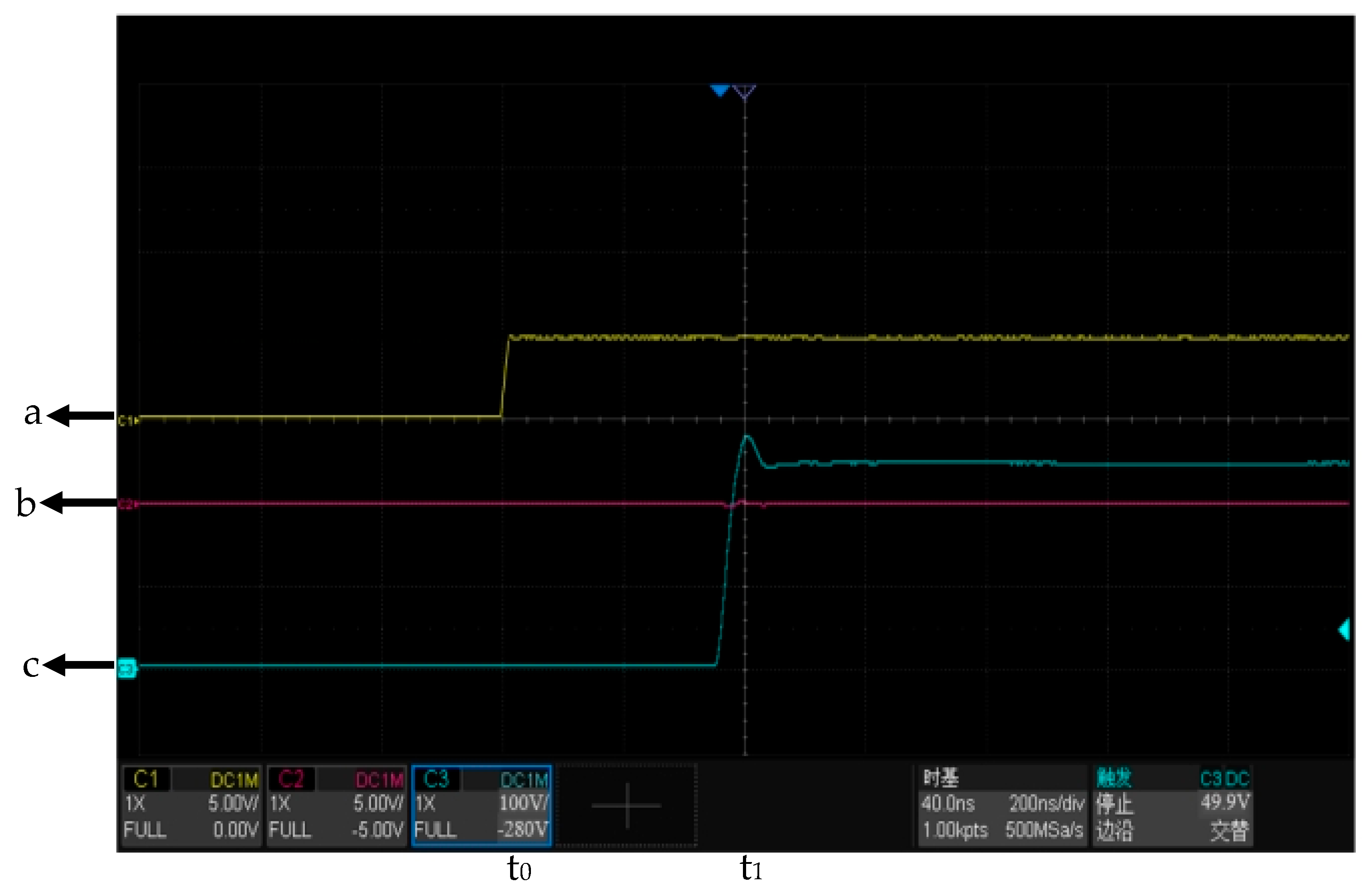
Figure 15.
Figure 15 shows the time delay of input and output signals for the driving circuit. In
Figure 15, t0 represents the time when the trigger signal is applied to pin IN1, and t1 represents the time when the 220 V output voltage is obtained at both ends of the coil. The time interval from t0 to t1 is the time delay of signal. In
Figure 15, the voltage per division of each channel remains unchanged, and the time setting is at 200 ns per division. As can be seen from
Figure 15, the time delay of input and output signals is approximately 400 ns. The experimental result proves that the response speed of the driving circuit is very fast.
The oscillogram at time t1 in
Figure 14 is stretched to obtain
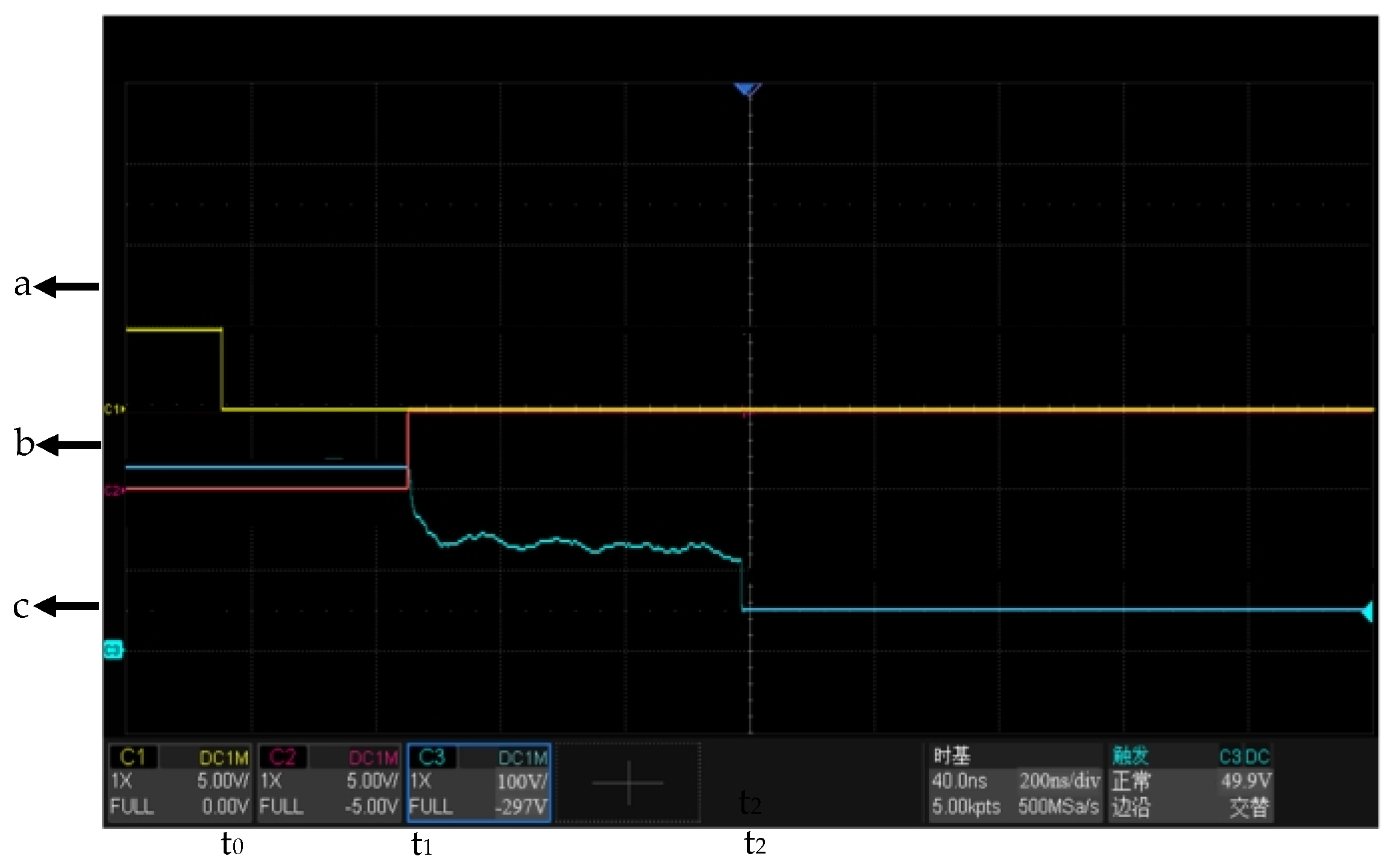
Figure 16.
Figure 16 shows the oscillogram of the high–low-voltage trigger signal switching time delay, and the voltage per division of each channel remains unchanged while the time setting is at 200 ns per division. In
Figure 16, t0 represents the time when the trigger signal of pin IN1 drops from a high level to a low level, and t1 represents the time when the trigger signal of pin IN2 rises from a low level to a high level. Furthermore, t2 represents the time when the 50 V output voltage is obtained at both ends of the coil. As can be seen from
Figure 16, the switching time delay of the trigger signals between pins IN1 and IN2 is approximately 500 ns, and the switching time delay of the voltage signal at both ends of the coil drops from 220 V at time t1 to 50 V at time t2 is about 600 ns. The waveform of the switching process fluctuates slightly, and it is mainly caused by the contact bouncing when the micro relay switches from RL1 to RL2.
5.2. Experimental Testing of the Silicon Controlled Rectifier Driving Circuit During the Switch-Off Process
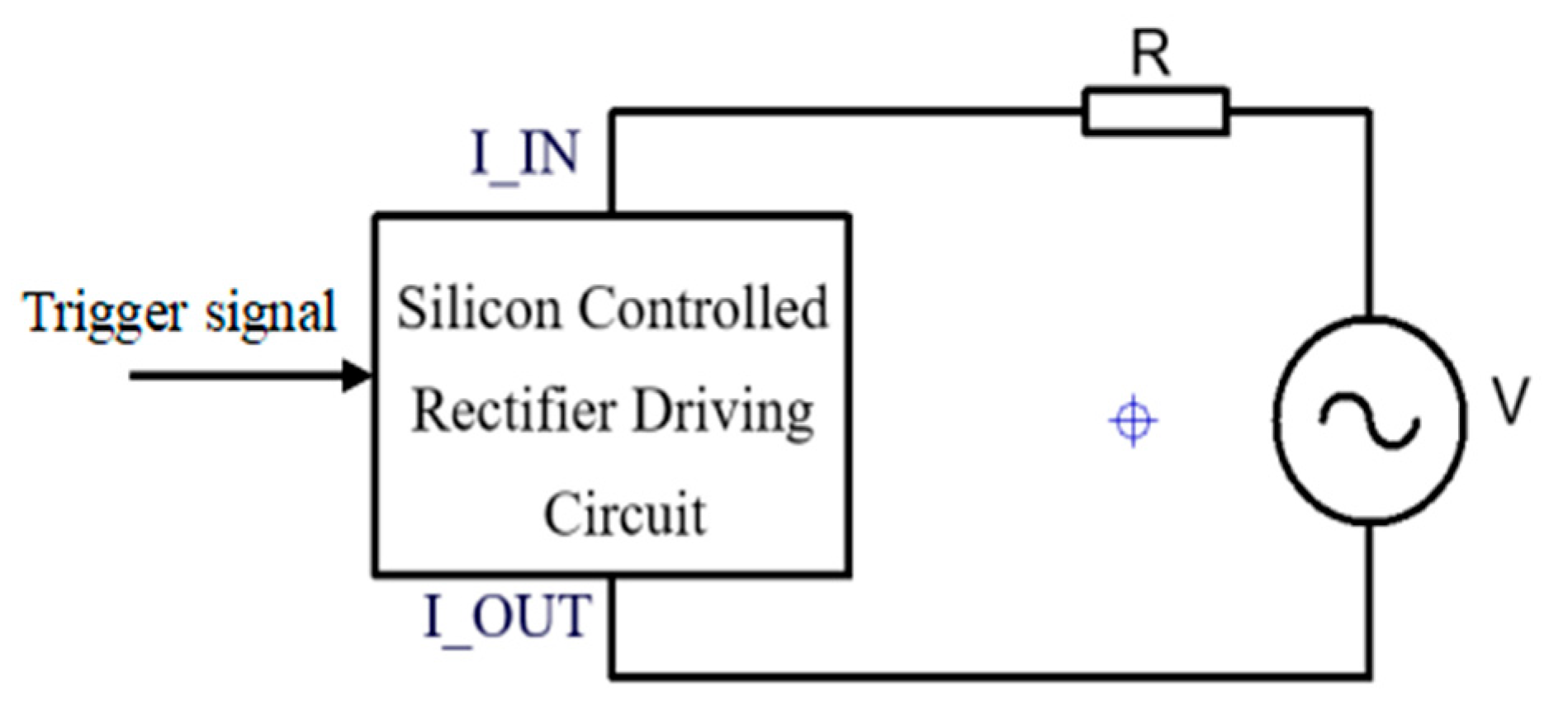
The resistor R and an AC power supply are connected in series between I_IN and I_OUT of the silicon-controlled rectifier driving circuit in
Figure 4. The testing scheme is shown in
Figure 8.
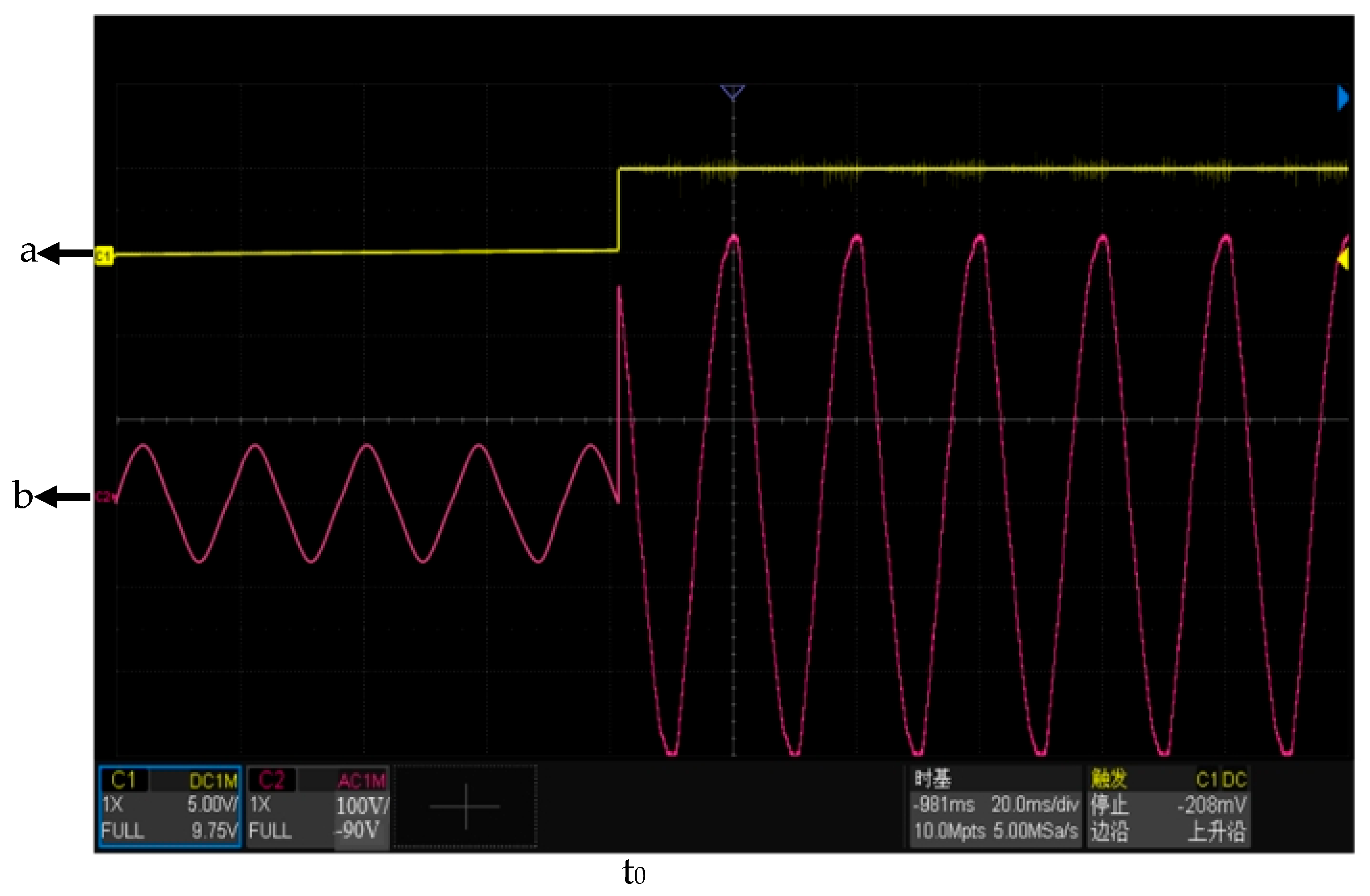
Figure 17 shows the oscillogram of the experimental testing for the silicon-controlled rectifier after receiving the gate trigger signal.
In
Figure 17, channel 1 of the oscilloscope measures the trigger signal of pin IN1, and the voltage setting is at 5 V per division. Meanwhile, channel 2 of the oscilloscope measures the voltage signal across the resistor R, which is connected in series with the silicon-controlled rectifier driving circuit, and the voltage setting is at 100 V per division. Furthermore, the time setting is at 20 ms per division. As can be seen from
Figure 17, the trigger signal of pin IN1 rises from a low level to a high level at time t0, and the silicon-controlled rectifier can immediately conduct. The AC voltage across the resistor R changes from a minor amplitude to a higher amplitude. Because the gate trigger signal remains constant, the silicon-controlled rectifier can still continue to conduct after the AC voltage changes from the positive half cycle to the negative half cycle.
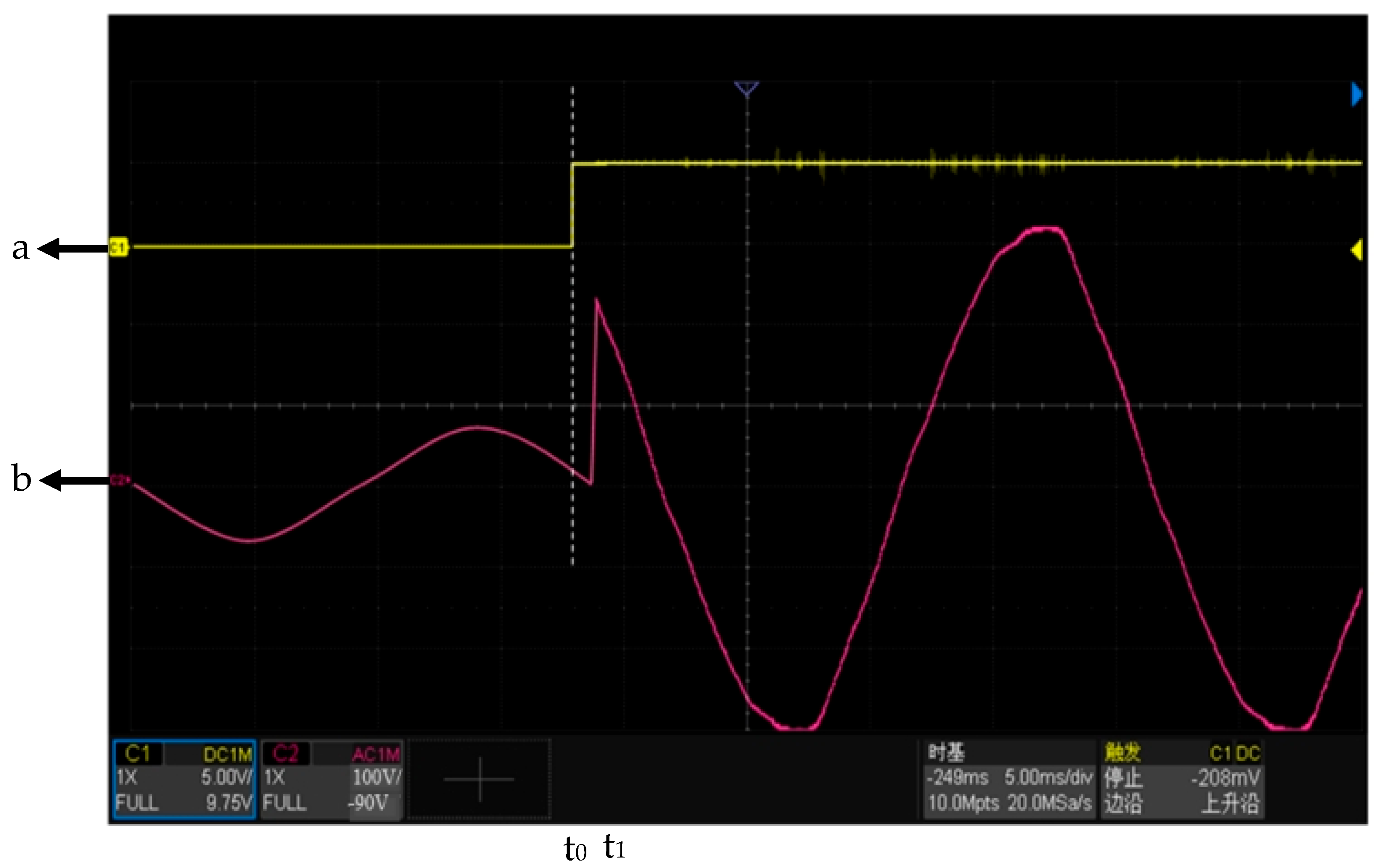
The oscillogram at time t0 in
Figure 17 is stretched to obtain
Figure 18, and the voltage per division of each channel remains unchanged while the time setting is at 5 ms per division. As can be seen from
Figure 18, the voltage across the resistor R changes at time t1 after pin IN1 receives the trigger signal at time t0, and the conduction time delay between the anode and cathode is less than 1 ms. The result of the experimental testing shows that the response speed of this driving circuit is very fast and meets the design requirement.
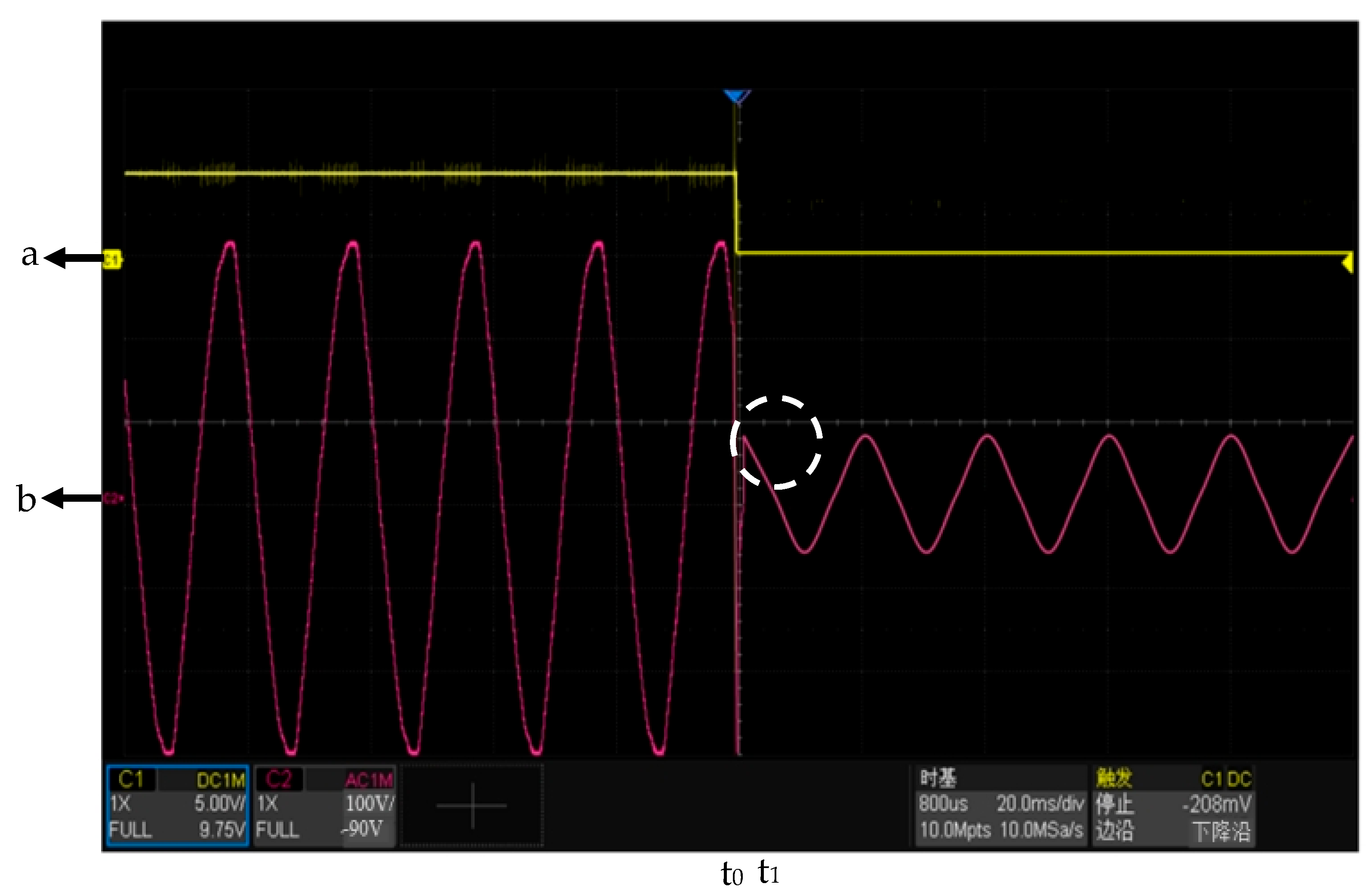
Figure 19 shows the oscillogram of the experimental testing for the silicon-controlled rectifier after losing the gate trigger signal, and the parameters measured by each channel of the oscilloscope remain unchanged. As can be seen from
Figure 19, the trigger signal of pin IN1 reduces from a high level to a low level at time t0. Meanwhile, the current flowing between the anode and cathode of the silicon-controlled rectifier approaches the zero-crossing point at time t1 (it is indicated by the dotted circle). Therefore, the current flowing between the anode and cathode of the silicon-controlled rectifier is less than the holding current; then, the silicon-controlled rectifier is turned off. Hence, the AC voltage across the resistor R changes from a higher amplitude to a minor amplitude. The experimental testing result shows that the driving circuit designed above can undertake the shunting effect and verify the correctness of the driving circuit of an AC contactor during the switch-off process.
5.3. Experimental Testing of the Three-Phase Signal Acquisition Circuit
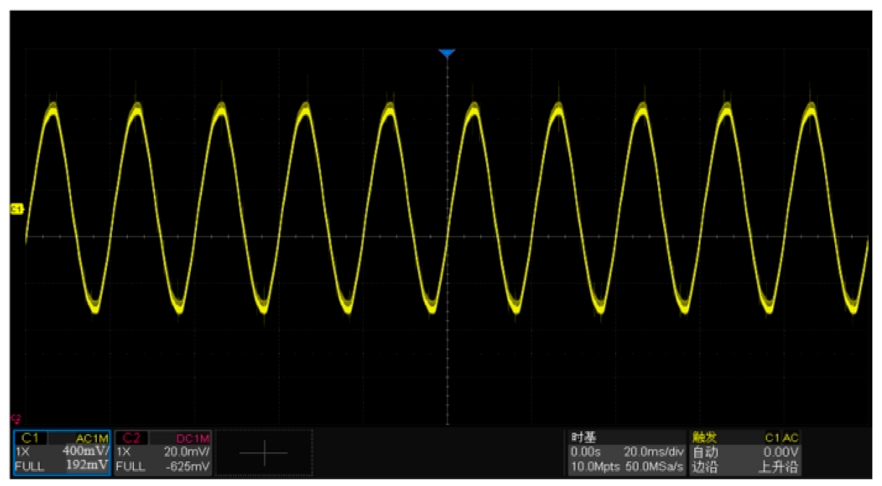
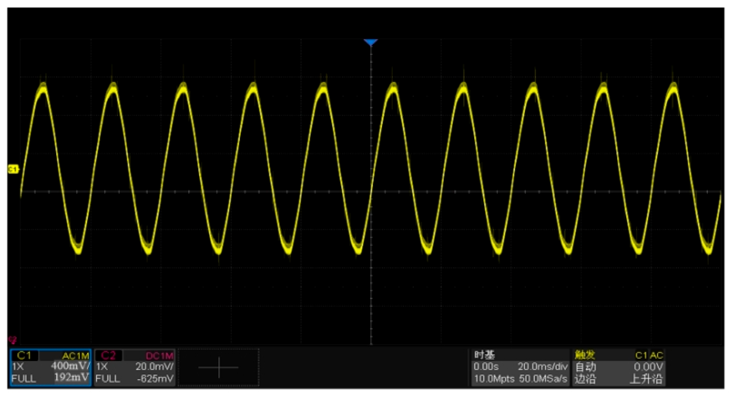
Figure 20 and
Figure 21 show the output waveforms of the experimental testing for the three-phase voltage acquisition circuit under 220 V AC voltage and the three-phase current acquisition circuit under 5 A AC current, respectively. The testing results are both represented by the voltage waveform across the resistance R6. In addition, the voltage setting is at 400 mV per division, and the time setting is at 20 ms per division. As can be seen from
Figure 20 and
Figure 21, the output voltage amplitudes of the three-phase voltage acquisition circuit and three-phase current acquisition circuit are both approximately 0.8 V, which meet the design requirements.
