1. Introduction
Electric-double-layer-gated transistors (EDLTs) have gained attention for their ability to induce high capacitance densities (~µF cm
−2) and large sheet carrier densities (~10
14 cm
−2) [
1,
2,
3] while also exhibiting dynamic synaptic properties that mimic biological learning processes [
4,
5,
6,
7], making them a promising candidate for next-generation energy-efficient computing applications including neuromorphic computing [
8,
9,
10]. In an EDLT, ions migrate under an applied electric field through an ionically conductive but electrically insulating electrolyte, accumulating at the interface of a channel material, typically a semiconductor. This forms an electric double layer (EDL) comprising a closely packed ionic layer in the electrolyte and an induced charge layer in the semiconductor, effectively creating a sub-nanometer-gap capacitor. Such an arrangement allows charge accumulation of ~10
13–10
14 cm
−2 in graphene [
11,
12] and transition metal dichalcogenides (TMDs) [
13,
14,
15], as measured by the Hall effect. These charge densities correspond to capacitance values ranging from a few µF cm
−2 [
12,
15] to tens of µF cm
−2 [
12,
15], surpassing conventional oxide dielectrics and enabling access to transport regimes otherwise difficult to achieve, including gate-induced superconductivity [
14,
16], metal-insulator transitions [
17], and unconventional charge transport phenomena [
18].
Two-dimensional (2D) crystals are ideal channel materials for EDLTs due to their atomically thin nature, which ensures that all charge carriers reside near the interface, maximizing their sensitivity to ionic accumulation at the surface. Small variations in ion density can induce orders-of-magnitude changes in the electrical resistance of 2D materials [
19,
20,
21]. Additionally, 2D crystals exhibit high mobility, tunable band structures, and strong electrostatic responsiveness, making the combination of 2D crystals and ions promising for neuromorphic computing, low-power electronics, and reconfigurable optoelectronic devices [
9,
18,
22]. Therefore, understanding ion–electron interactions and optimizing capacitance at the electrolyte/2D crystal interface are essential for advancing EDLT-based applications.
The total capacitance in 2D-crystal-based EDLTs is typically modeled as a system of capacitors in series, comprising geometric capacitance (C
G) and quantum capacitance (C
Q), the latter arising from the finite density of states (DOS) in 2D crystals. However, experimental studies have revealed deviations from this conventional sum, suggesting an additional contribution termed cross-quantum capacitance (CQC) [
15,
23]. CQC originates from charge screening interactions between the accumulated charge in the semiconductor and counterions in the electrolyte. Given that these charge layers are separated by ~1 nm or less, mutual screening effects can significantly influence the total capacitance. Because the performance of EDLTs relies critically on interfacial capacitance, accurately capturing these mutual screening effects through CQC is essential for understanding fundamental ion–electron interactions and optimizing device design and performance. For example, Zhang et al. observed a non-monotonic dependence of total capacitance on charge separation distance [
15]. This suggests that introducing a dielectric spacer within the EDL and thereby increasing the distance between ions and electrons could, counterintuitively, increase rather than decrease the total capacitance [
15,
24,
25].
This study examines the theoretical framework of CQC and its impact on EDLT performance. We first review CQC fundamental principles and theoretical models, then compare experimental observations with analytical frameworks incorporating cross-layer charge screening to determine conditions under which CQC modifies capacitance behavior. Furthermore, we explore scenarios where CQC may lead to unexpected capacitance increases, offering insight into the fundamental electrostatic properties of EDLTs. By elucidating the mechanisms governing CQC, this work aims to advance the understanding of charge screening in ion-gated transistors and provide guidelines for optimizing their capacitive performance in emerging electronic applications.
2. Background and Theory
The theoretical framework for CQC was originally developed by Berthod et al. [
23]. In this section, we summarize the key elements of their model to provide conceptual clarity and highlight specific features that are essential for the analyses and discussions that follow.
Traditional quantum capacitance (TQC) arises from the finite density of states (DOS) in a material. To illustrate this, we consider a two-dimensional electron gas (2DEG), where the wave function is free in
or
but confined in
. Through the geometric superposition of one-dimensional wave functions, we can determine the overall wave function in Equation (1), with energy eigenvalues given in Equation (2):
In the equations above,
(where
i =
x,
y,
z) represents the length of the system in the corresponding spatial direction, and
is the principal quantum number associated with confinement in the
direction. Through the wave function, the development of a two-dimensional reciprocal space is apparent. Assuming periodic boundary conditions in an infinite well, we know the quantized value of
and its change between
values, as given in Equations (3) and (4):
The size of the overall
-state in reciprocal space is then
. Because the energy of the system is ambivalent to the sign of either
component, the area of
-space considered when determining the DOS is therefore the area of an infinitesimal ring, given by
. It is necessary to note that the energy in Equation (2) can be put into two terms: a
-dependent term and the
-dependent term
. By subtracting
, we can create a relationship between
and the other energy terms, given in Equation (5):
The invocation of
implies that the density of states will be split into
subbands. Dividing the area by the size of
-state and putting
in terms of energy
via Equation (2) yields the DOS for a 2D electron gas:
In this case,
is the Heaviside step function, and summing over
yields the value of
for multiple subbands. Using this result, with units of
, one can surmise the amount of energy added to a system through the addition of
charge carriers to a given subband in a given area. This energy, the change in the chemical potential
, is found in Equation (7).
This relation can be used in conjunction with the definition of total capacitance
per unit area, as given in Equation (8), which is derived from the curvature of the energy–charge relationship, to determine the TQC [
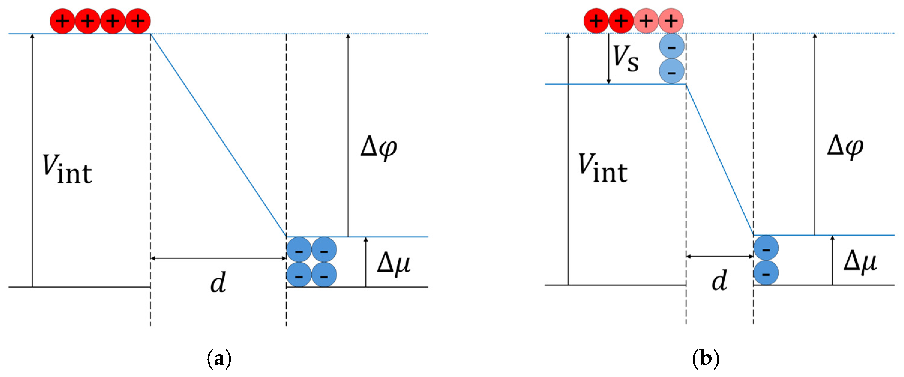
23]. This contribution to the total capacitance, alongside the equation for geometric capacitance in Equation (10), is depicted in
Figure 1a. It is important to note that the geometric capacitance depends solely on electrostatic potential
and charge density
.
However, the conventional treatment of quantum capacitance represents only one part of the complex interplay of effects occurring at the nanoscale. In addition to TQC, electron correlation and exchange energies contribute to the overall energy
described in Equation (8), complicating the determination of total capacitance. These complexities create conditions under which CQC can emerge, particularly at small inter-plate distances
, where geometric capacitance becomes exceptionally large (
Figure 1b). Such conditions are predicted to occur in EDLTs, where the ions and their induced image changes in the EDL are typically separated by less than 1 nm [
1,
2]. Experimental reports of CQC have been observed under conditions where the geometric capacitance is large, thereby reducing its relative influence in the total series capacitance. In such cases, the contributions from TQC and CQC become more prominent in determining the overall capacitance behavior [
15,
24,
25].
To analyze the regime in which CQC emerges, it is useful to treat the system’s capacitance as a linear response to a small perturbative energy
, rather than attempting to explicitly account for all microscopic energy contributions. This motivates the application of linear response theory. For symmetry, the energy perturbation is applied as
to opposite sides of the capacitor, which throughout this work we refer to as Plate 1 and Plate 2. We retain the two-dimensional wave vector from the traditional analysis and assume the charge sheets are separated along the real-space
dimension. The Kubo formula, given in Equations (11a) and (11b), is then used to evaluate changes in the number density operator
(as opposed to charge density) [
26].
Here, denotes the retarded correlation function, defined in terms of the Heaviside step function and the time-dependent commutator between an arbitrary operator and the perturbed Hamiltonian . The brackets indicate an equilibrium average with respect to the unperturbed Hamiltonian at equilibrium. That is, via this relation, , a non-equilibrium quantity after , has been expressed in terms of the retarded correlation function of the system in equilibrium.
These equations describe how the expectation value of an operator
evolves following the application of a perturbation at time
, exhibiting linear behavior to first order. Equation (12) defines the perturbation Hamiltonian
for our system [
5].
Evaluating the retarded correlation function in Equation (11b) reveals that the resulting commutator term is proportional to the commutator of number density operators. This retarded correlation function defines the system’s susceptibility, directly analogous to the susceptibility
in classical electromagnetism, which quantifies linear polarization in response to an applied electric field. This analogy is intuitive: the excess charge determined by linear response theory corresponds to the system’s induced charge [
26]. With this in mind, we can write the change in a number density operator through Equation (11a) in terms of
[
23]:
Converting the excess induced charge into a capacitance is straightforward using the relation
[
23]. Because the induced charge must be the same regardless of whether it is computed from Plate 1 or Plate 2, we can relate the susceptibilities as follows:
To proceed, we treat
as a single-particle Green’s function [
26] and apply the Dyson equation, where the perturbation is the Coulomb potential
, and the bare Green’s function is the irreducible polarizability
:
Unlike susceptibility, the irreducible polarizability
does not have a classical analog, as it remains finite even in the absence of an external perturbation [
15]. Solving Equation (15) is nontrivial, as
,
and V are all matrices. Diagonal elements of
describe intra-plate screening, while off-diagonal terms capture inter-plate—or cross-capacitive—effects. These off-diagonal terms are key to the emergence of CQC.
To arrive at an expression for the total capacitance that includes these effects, it is necessary to introduce a screened interaction potential. This potential can be interpreted as a Green’s function where the perturbation is the polarizability
and the bare interaction is the unscreened Coulomb potential [
23]. The full expression for the capacitance, incorporating both geometric and quantum contributions, is then:
This expression makes explicit the role of cross-plate interactions. When the off-diagonal terms are small (or neglected in the case of the random phase approximation), the remaining terms reduce to the standard density-of-states-derived expression for TQC [
23]. Determining the polarizabilities for a given system is challenging, but Berthod et al. developed a set of approximations that are potentially applicable to systems with dissimilar charge carriers, such as EDLTs (e.g., ions and electrons in EDLs). These approximations are discussed and analyzed in detail in the remainder of this work. It should be noted, however, that while these approximations have been adopted as theoretical support in several experimental works [
15,
24,
25], Berthod et al. noted in their original work that their model was not explicitly developed for EDLTs [
23].
Equations (17a–d) define the polarizabilities used in the model [
23] and in this study. It is important to point out that Equations (17c) and (17d) are coupled and should be solved self-consistently. The Equations are functions of nine parameters, defined in
Table 1. All parameters are unitless except for
, which has units of length. Also of note, the Bohr radius
presented in
Table 1 is the two-dimensional Bohr radius, which is widely used in modeling the excitonic and electrostatic properties of 2D materials [
23,
27,
28,
29]. It arises from the analytic solution of a hydrogen-like system confined to two dimensions, resulting in a modified Coulomb potential and a distinct prefactor compared to the three-dimensional case.
3. Results and Discussion
A key experimental implication of CQC proposed in prior studies is the substantial reduction in total capacitance at the EDL interface due to interlayer charge screening effects [
15]. Follow-up experimental efforts have explored the insertion of a spacer layer between the EDLs as a means to mitigate this reduction and enhance the total capacitance [
24,
25]. Theoretically, such enhancement is possible if the total capacitance exhibits a non-monotonic dependence on the inter-plate distance, a behavior predicted in the model proposed by Berthod et al. [
23]. To better understand the conditions under which this non-monotonic behavior can arise, we evaluated the influence of the model parameters,
and
.
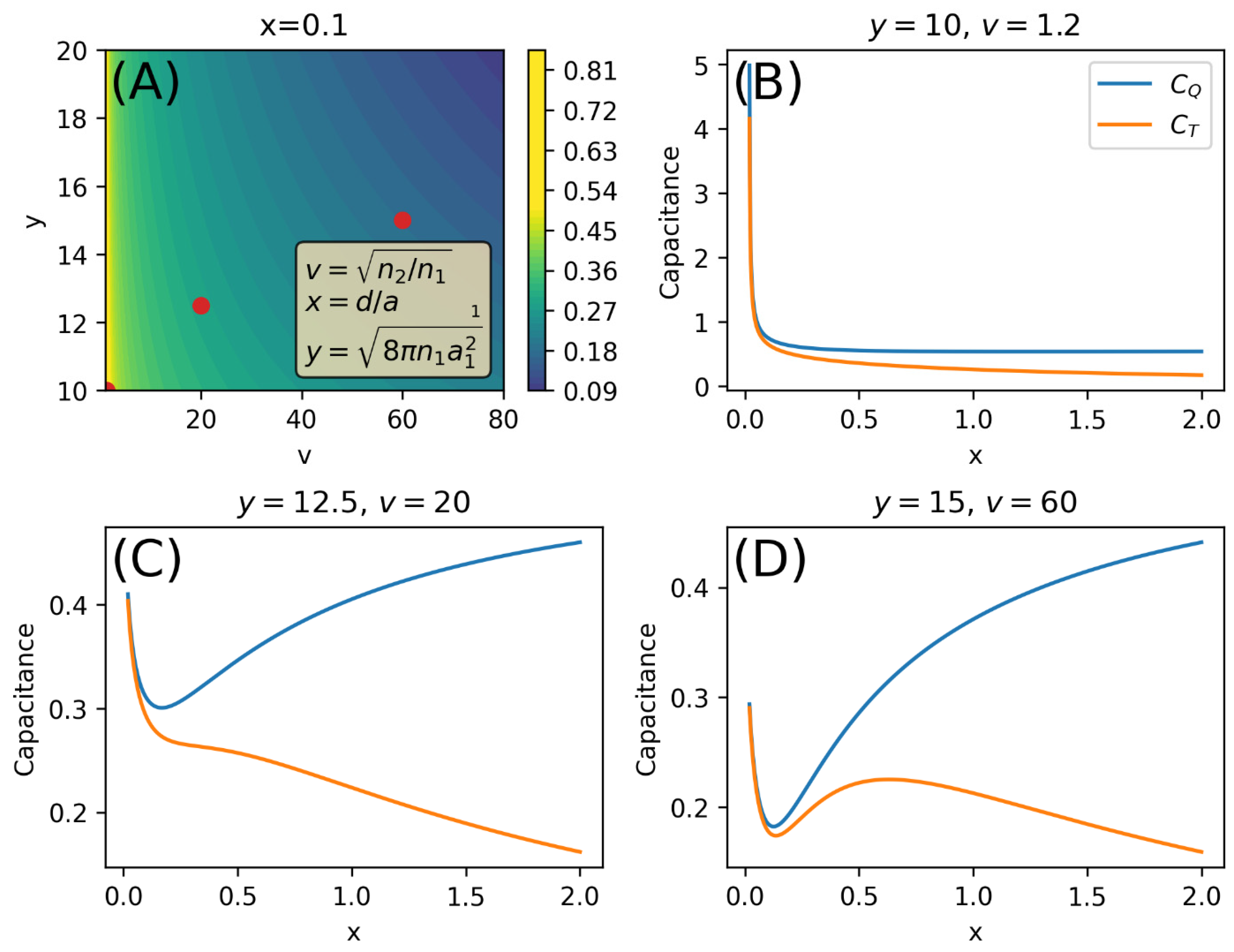
We first fix
to be 1 (
and set
to 0.1 to represent a near-zero inter-plate distance. Capacitance values were then computed across various combinations of
and
, with results shown in
Figure 2. In these evaluations, regions exhibiting low capacitance at small
were considered most likely to support non-monotonic behavior with respect to increasing distance—a hypothesis that is later validated. For this initial analysis, we focused on the
parameter space while holding
constant.
Figure 2B–D show the
-dependence of capacitance for the three
combinations indicated by the red dots in
Figure 2A. These projections confirm the trend observed in the contour map: higher values of
and
increase the likelihood of observing non-monotonic behavior. Experimentally, this suggests that such effects are more likely to appear in systems with (1) high charge dissimilarity between the plates and (2) high carrier concentration on Plate 1. While EDLTs are capable of supporting high carrier densities, achieving a large inter-plate charge ratio (i.e., high
) may be difficult because the induced charge in the channel generally mirrors the ionic charge in the electrolyte. This poses the first challenge for experimentally realizing the non-monotonic regime predicted by the model.
In
Figure 2D, a clear capacitance peak appears at
. The corresponding physical separation depends on the Bohr radius
, as defined in
Table 1. For example, if
, this distance is approximately 17 pm, whereas for
, it extends to 170 nm. This highlights the wide range of spatial scales that can result from different effective masses in experimentally chosen material systems. Importantly, separations on the order of tens of picometers may be difficult to achieve or reliably control in experiments. This underscores the importance of careful material selection and the precise tuning of system parameters when attempting to probe CQC in the narrow window where non-monotonic behavior is predicted to occur. While the non-monotonic
behavior shown in
Figure 2D is consistent with the prediction in previous experimental EDLT studies [
15], our results suggest that realizing such effects may be experimentally challenging and limited to highly constrained regimes.
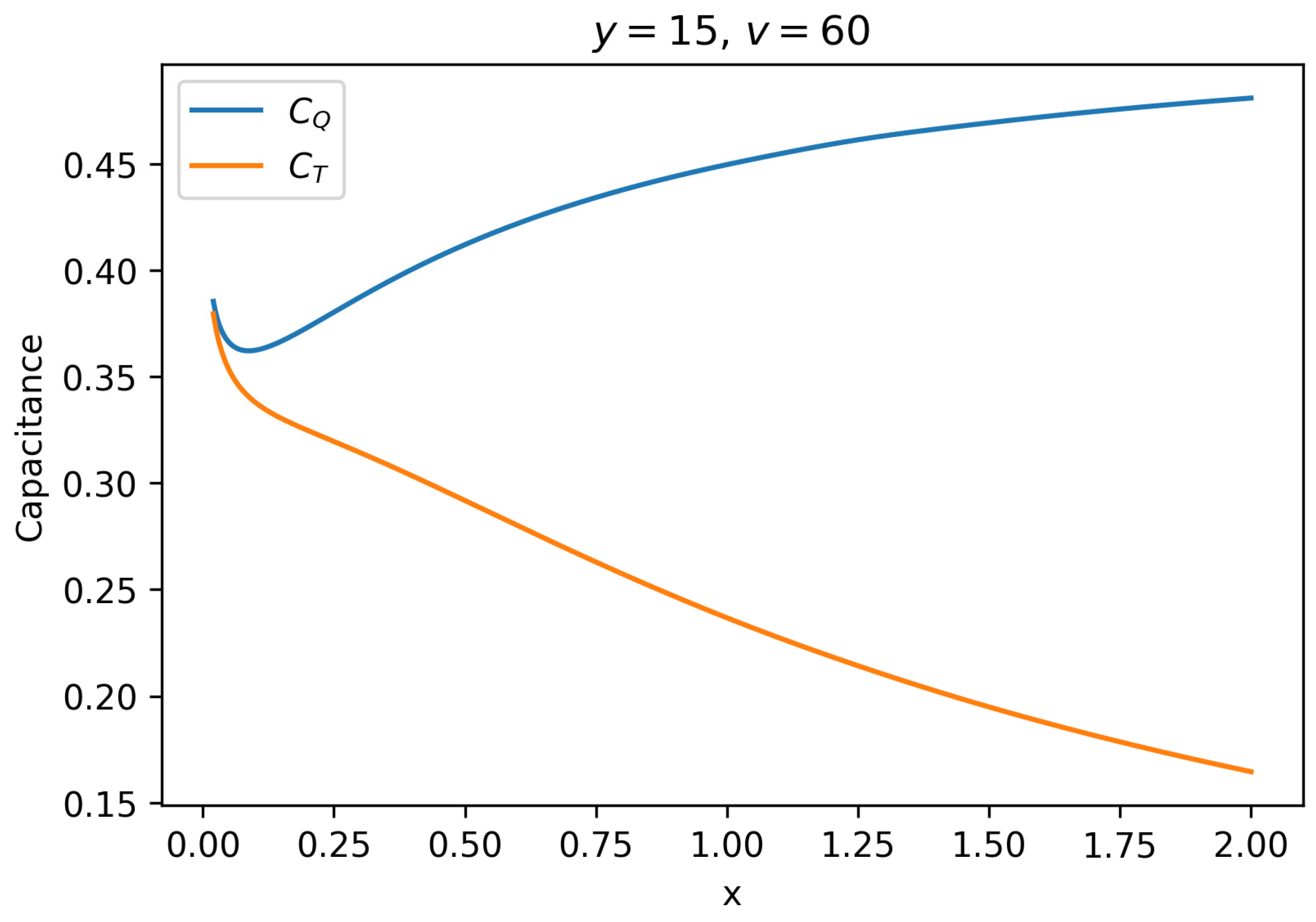
Additionally, as noted in
Section 2, Equations (17c) and (17d) are coupled and should be solved self-consistently. When the system is treated self-consistently by iterating Equations (17c) and (17d), the non-monotonic signature largely disappears. The resulting
-profile, shown in
Figure 3, exhibits a more monotonic behavior. Equations (17c) and (17d) were iterated 1000 times for each parameter set. We observed that the capacitance values stabilized well before this point, and additional iterations produced negligible change, indicating effective convergence.
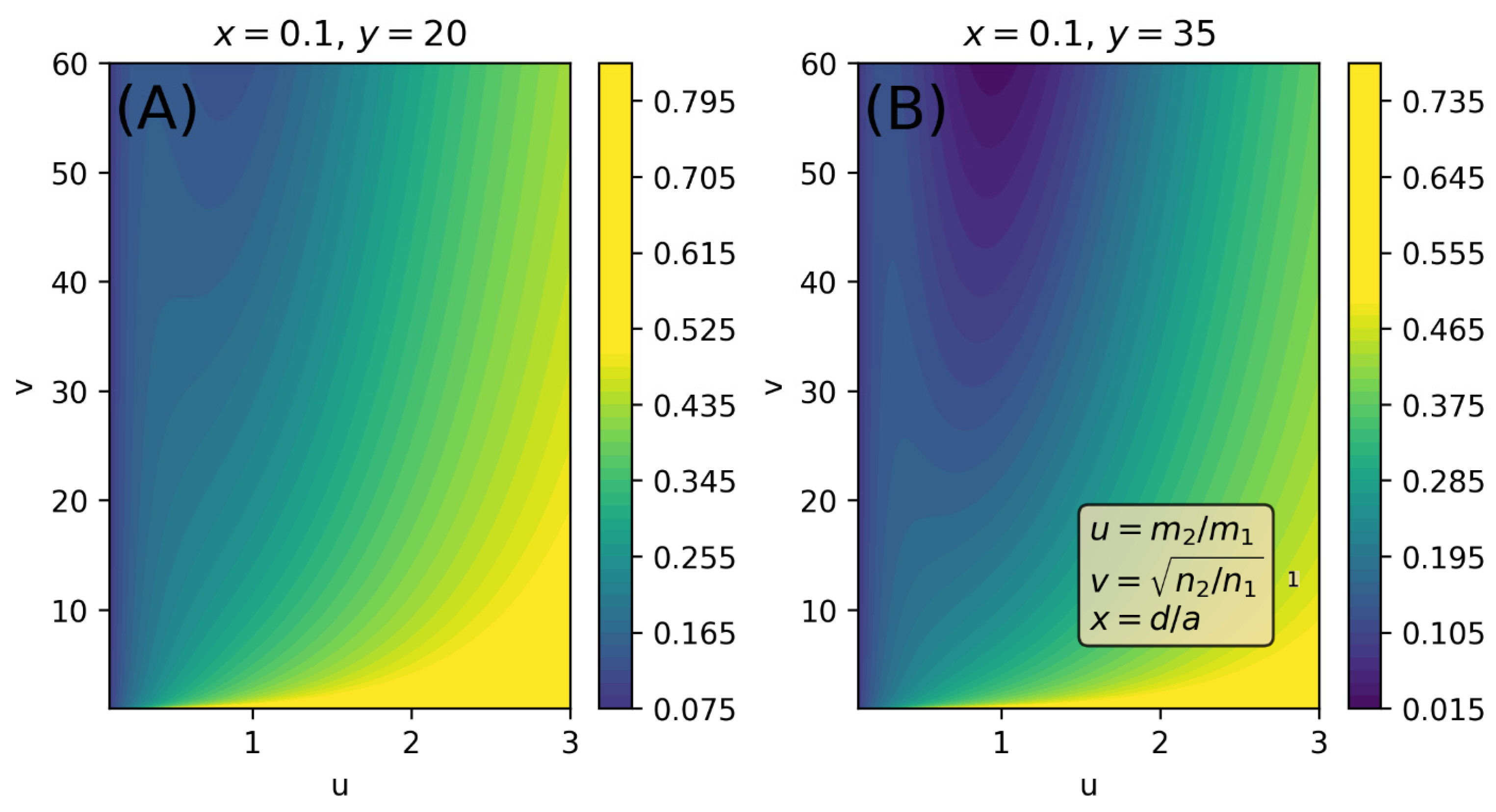
This trend holds across other parameter spaces as well. For instance, the
parameter space, shown in
Figure 4A,B for different fixed values of
, indicates that increasing
expands the range of
over which capacitance is suppressed—consistent with the behavior observed in the
parameter space.
The overall trends in
Figure 4A and
Figure 4B are qualitatively similar, with the region of lowest capacitance consistently centered around
. This implies that non-monotonic behavior is most likely when the effective masses of carriers on both plates are identical. This observation is further supported by the
projections in
Figure 5, which show that the non-monotonicity gradually diminishes as
increases from 1 to 3. The limited parameter space for observing non-monotonic capacitance behavior results directly from the restrictive assumptions and parameter definitions embedded within the original theoretical model. In practice, however, achieving similar effective masses between ions and their induced image charges may be difficult, particularly in typical EDLTs where the ions and induced charge carriers (i.e., electrons or holes) have fundamentally different physical properties.
In presenting the model, Berthod et al. state clearly that the model is only valid for metallic systems with ideal 2D electron gases [
23]. However, they mentioned that the qualitative insights it offers may still be relevant to understanding CQC in EDLT systems, and several follow-up experimental studies have adopted their model for theoretical interpretation [
24,
25]. To examine this applicability, we evaluated the model under conditions representative of experimental EDL interfaces. As a pedagogical case, we considered lithium ions (Li
+) inducing a charge on a graphene channel. We chose this material system for three reasons. First, graphene is a well-established 2D material for EDL gating with Li
+, as demonstrated in multiple experimental studies [
30,
31,
32,
33,
34]. Second, our analysis shows that a high carrier concentration on the channel side enhances the impact of CQC, and prior experimental studies have demonstrated that EDL gating on graphene can induce carrier densities on the order of
cm
−2 [
11]. Third, the characteristic separation for observing CQC depends on the effective mass of the channel material. For
, this distance is on the order of tens of picometers—experimentally difficult to access. Graphene’s much smaller effective mass shifts this scale to hundreds of nanometers (e.g., 170 nm if assuming
), making it a more favorable platform for probing CQC. Because the EDL interface typically involves each ion inducing an equal and opposite image charge in the channel (e.g., one cation induces one electron in the channel), we assume a near-unity charge ratio between the two plates.
Estimating the effective mass in EDL systems is challenging. While effective mass is routinely used to describe the band dynamics of electrons and holes in crystalline solids, it is rarely applied to ions like Li
+, whose transport is dominated by thermally activated hopping or diffusion rather than coherent, band-like motion. Nevertheless, a rough estimate can be made by considering the rest mass of a lithium ion (
1.163 × 10
−26 kg, [
35]) and expressing it in units of the electron rest mass,
. Although this estimation does not reflect the underlying transport physics of Li
+, it provides a pragmatic way to approximate the large mass asymmetry typical of EDL systems and evaluate its effect on CQC.
The effective mass of charge carriers in graphene is also difficult to define due to its linear energy–momentum dispersion and massless Dirac fermion behavior. Reported values vary from approximately 0.01 to 0.07
, depending on the number of layers (i.e., single layer vs bilayer graphene) and influenced by factors such as electron–electron interactions, carrier density, and disorder not captured by the ideal Dirac model [
36,
37,
38]. In the first pedagogical case, we assumed an effective mass of
, which corresponds to a phenomenological value often used to represent high carrier mobility and a low density of states near the Dirac point in gated graphene.
Notably, the parameter values chosen to reflect experimental EDL systems do not satisfy the criteria previously identified in this study for producing non-monotonic capacitance behavior (i.e., the effective masses of carriers on both plates must be identical). As shown in
Figure 6, no non-monotonicity is observed—consistent with expectations. However, contrary to the predictions of Zhang et al. [
15], in this case, the total capacitance obtained when accounting for both TQC and CQC (
is not lower than that predicted by TQC alone (
. In fact, with the effective masses assumed for graphene and Li
+,
exceeds
. In the limiting case of
, the two results converge, as expected.
It is worth noting that the parameter values chosen in
Figure 6 fall outside the screening condition outlined by Berthod et al., which demands that
[
23]. Nonetheless, similar trends can be observed in other pedagogical cases. From Equations (16) and (17), we can argue that in physically realistic systems where
(i.e., each ion inducing an equal and opposite image charge in the channel), the inter-plate polarizabilities
and
can be minimized while simultaneously maximizing the intra-plate terms
. As
, accounting for CQC leads to a substantial increase in the total quantum capacitance (both CQC and TQC), allowing the total capacitance
to approach the geometric limit
.
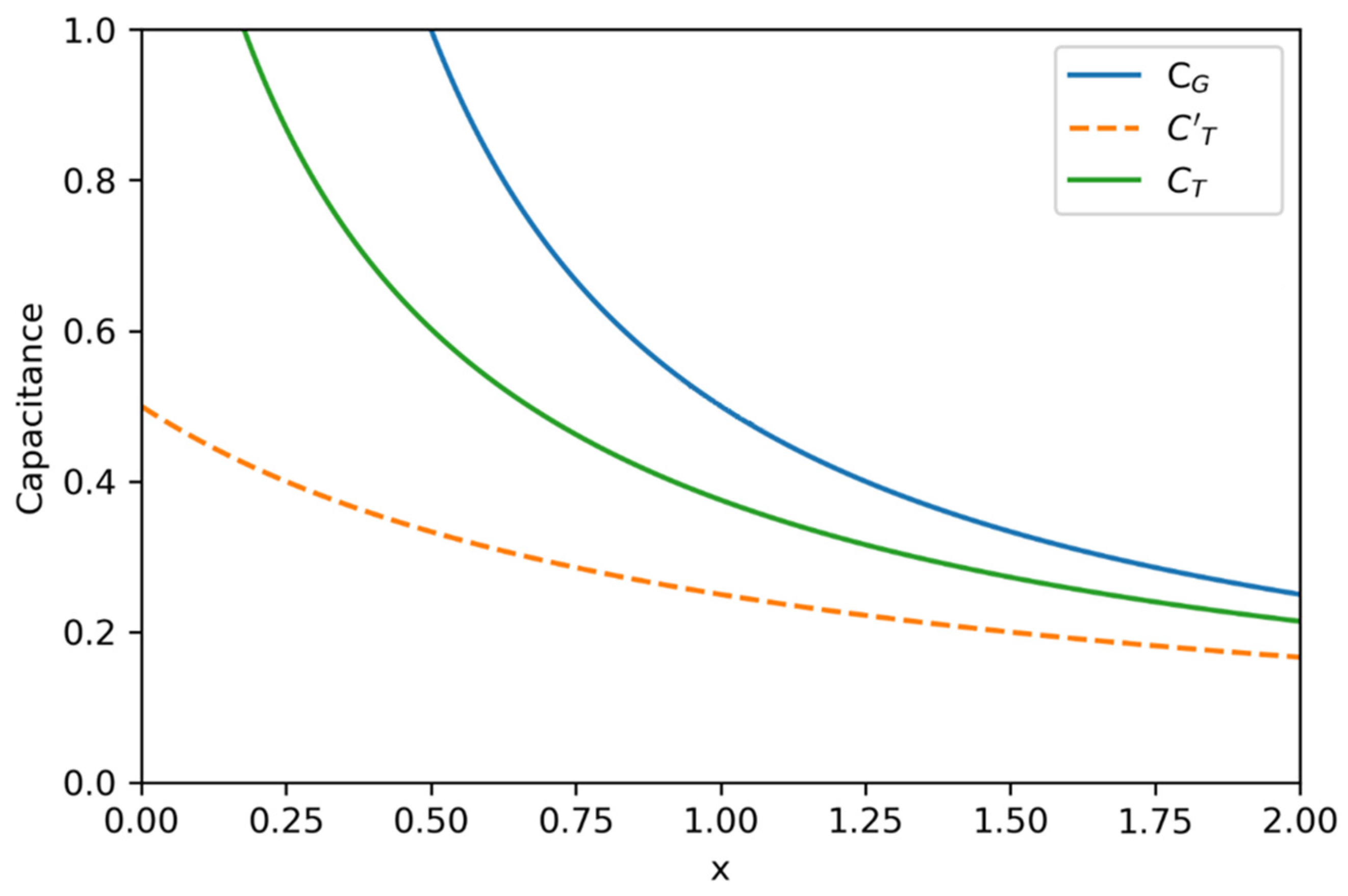
Figure 7 illustrates one such case, with
and
, where
is significantly enhanced over the TQC-only result
.
The required physical separation for observing this enhancement is also experimentally accessible. For instance, if assuming
, consistent with prior experimental estimates for single-layer graphene [
36], the
normalized distance corresponds to a real-space separation of
nm. This scale is within the range of current fabrication techniques, such as dielectric deposition or 2D heterostructure assembly [
39,
40]. This result demonstrates that CQC can still enhance total capacitance under conditions that are more experimentally attainable than those required to produce non-monotonic behavior. It highlights a promising pathway for probing and leveraging CQC without the need for exotic material parameters or extreme device geometries.
It should also be emphasized that non-monotonic effects are largely suppressed in self-consistent solutions. This suggests that any observable non-monotonicity is likely to be subtle and easily masked by experimental noise or interface imperfections. As a result, the proposed increase in capacitance via the introduction of spacer layers—suggested in prior studies [
24,
25]—may be difficult to observe experimentally. Moreover, systems such as EDLTs, which involve dissimilar charge carriers (e.g., ions and electrons), operate under strong coupling and non-equilibrium conditions and thus lie outside the original assumptions of the CQC model. The model was developed for ideal, metallic 2D electron gases in equilibrium, and as illustrated in this study, the predicted non-monotonic behavior occurs primarily when the effective masses of carriers on both plates are identical—conditions that do not fully reflect the distinct transport properties and ion–electron interactions typical of EDL interfaces. Nonetheless, when applied as a qualitative test case, our results reveal that the total capacitance—including CQC—under conditions resembling experimental EDLTs either matches or exceeds predictions based solely on TQC. These findings highlight the need for new theoretical frameworks that explicitly and rigorously integrate ionic and electronic conduction, enabling a more complete description of quantum effects and electrostatic phenomena at the nanoscale.


