Article

Multibattery Charger System Based on a Multilevel Dual-Active-Bridge Power Converter

by
José M. Campos-Salazar
1,*,
Sergio Busquets-Monge
1,
Alber Filba-Martinez
1 and
Salvador Alepuz
2
1
Electronic Engineering Department, Universitat Politècnica de Catalunya, 08028 Barcelona, Spain
2
Tecnocampus, Universitat Pompeu Fabra, 08302 Mataró, Spain
*
Author to whom correspondence should be addressed.
Electronics 2025, 14(8), 1659; https://doi.org/10.3390/electronics14081659
Submission received: 10 March 2025 / Revised: 12 April 2025 / Accepted: 14 April 2025 / Published: 19 April 2025

Abstract

:
This work introduces a novel battery charger implemented with a four-level three-phase neutral-point-clamped converter and a four-level single-phase dual-active-bridge converter, which offers the intrinsic advantages of multilevel conversion, provides galvanic isolation and allows bidirectional power flow. A detailed and extensive modeling of the system is developed, together with the design of appropriate closed-loop control and modulation. The proposed system allows individual charging of each battery pack, ensuring that the full capacity of the battery bank is utilized, even when the battery packs have different state-of-charge levels, differ in nominal capacities, or use different chemistries. Furthermore, the proposed control system manages the overall DC-link voltage and ensures voltage balance across both DC-links in the system. The effectiveness of the proposed system configuration and control has been validated through simulations. The simulation results show good dynamic response in different operating scenarios, confirming the suitability, feasibility, and benefits of the proposed implementation and control approach.

1. Introduction

The role of batteries is becoming more and more important, given the technological evolution in recent years. With regard to the electric vehicle (EV), its rapid expansion [1,2] has intensified the demand for fast, efficient, and smart battery chargers, since the battery is the heart of the EV. Moreover, the use of smart bidirectional battery chargers enables the use of the energy stored in the batteries of the EV as a flexible energy storage unit in diverse applications, a system collectively known as vehicle-to-X [2,3,4,5,6,7,8], employed, for instance, to feed loads (vehicle-to-load, V2L) or to exchange energy with other vehicles (vehicle-to-vehicle, V2V), houses (vehicle-to-home, V2H), or the electric grid (vehicle-to grid, V2G).
Batteries can also be applied to enhance the integration of renewable energy sources into the power network. Since the energy production of renewable energy sources obviously depends on the weather, a battery energy storage system (BESS) [9,10,11] can be used to store the energy surplus when more energy is produced than necessary, to be used at a later time when there is energy consumption but no energy production. To do it, the BESS requires a smart bidirectional battery charger.
In the context described above, battery chargers must deal with increasingly complex requirements, including the management of diverse battery chemistries [9], voltages, and capacities, ensuring optimal performance in terms of efficiency, reliability, and adaptability [12,13], and meeting the corresponding standards [3,14].
Battery chargers have been extensively reported in the literature [2,3,15,16,17,18,19], where the most common approach is based on conventional two-level converters. Isolation is an usual requirement for battery chargers, which can be fulfilled by means of a bulky grid frequency transformer or preferably with a dual-active-bridge (DAB) converter [20], given its advantages of bidirectional power flow capability, soft-switching commutations, low cost, operational flexibility, and high efficiency [21]. DAB converters are particularly well suited for interfacing with EV charging stations and renewable energy storage systems, where operational flexibility and efficiency are critical [20].
Recent works [22,23,24] have demonstrated the feasibility and suitability of three-level DAB converters for battery charger applications. This topology offers the intrinsic advantages of a multilevel structure [25,26], voltage stress reduction on power semiconductors, harmonic distortion improvement, and converter efficiency increase together with improved voltage regulation and enhanced power quality, in comparison to the conventional two-level converters. These features are pivotal as EVs and renewable energy systems demand higher power densities, broader voltage ranges, and stricter efficiency targets.
The present work goes one step further and introduces a four-level battery charger (4L-BC) based on an extended DAB converter topology, which apparently has not been previously described in the literature. This manuscript presents a complete model of the system (switching model, large-signal averaged model, and small-signal linear model), together with the design of the proper modulation and closed-loop control. The proposed approach presents some significant characteristics, which are described below.
The four-level structure provides reduced voltage stress on semiconductor devices, leading to better reliability and longer component lifespans, and smaller harmonic distortion, resulting in improved power quality and reduced electromagnetic interference [26,27].
The closed-loop control and modulation algorithms play a key role in the proposed system. For the grid-side converter, power factor control, a low harmonic distortion of the grid current, and DC-link capacitor voltage balance [28] are achieved. For the DAB converter, the charge/discharge current across each battery pack can be precisely controlled [27].
This last feature is particularly relevant. Since the charge/discharge current can be particularized for each battery pack, this can be extremely useful in the case of heterogeneous batteries with different state-of-charge (SoC), chemistries, or capacities [29,30,31]. The proposed system allows for the efficient and independent regulation for each battery, optimizing the overall charging and discharging process and ensuring a proper SoC balance across the battery packs [27]. The ability to handle batteries with different SoCs is essential for achieving optimal energy utilization and prolonging battery lifespans.
In summary, this work contributes to the ongoing development of multibattery charging systems by offering a comprehensive analysis of the four-level DAB converter capabilities. Through detailed analysis and simulation, this study validates the 4L-BC as a possible solution for next-generation battery charging applications.
This manuscript is structured as follows: Section 2 introduces the proposed charger topology, highlighting its design features. Section 3, Section 4 and Section 5 develop the switching model, large-signal averaging model, and small-signal linear model, respectively. Section 6 describes the control system design and the modulation algorithms and provides the system transfer functions. Section 7 presents the system stability analysis and the time-domain simulation results, offering insights into system behavior under various operating conditions. Finally, Section 8 concludes the manuscript by summarizing the key findings and contributions.

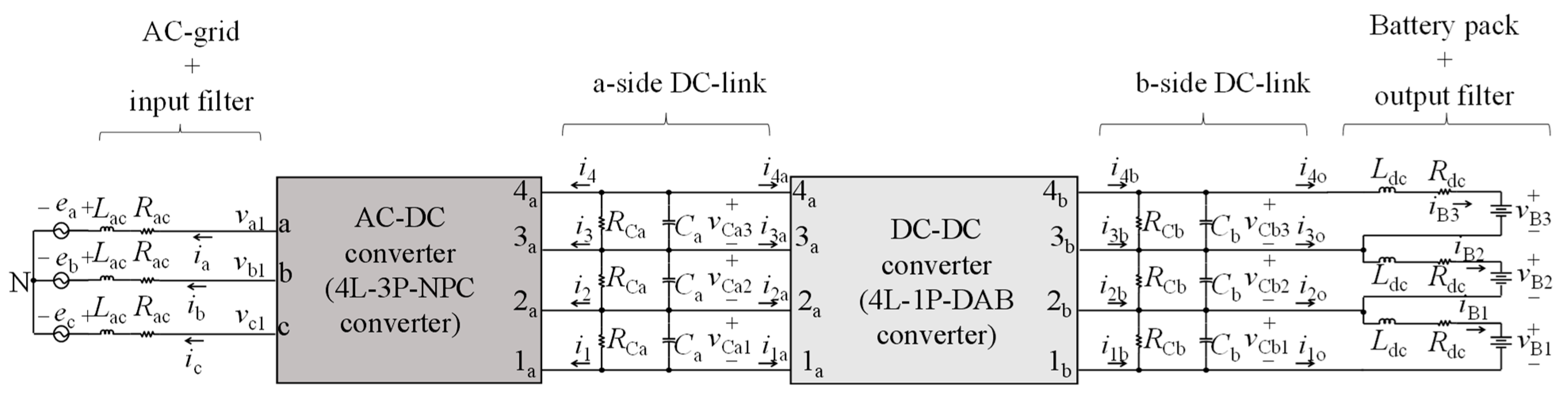
2. Battery Charger Topology

Figure 1 illustrates the topology and circuit model of the proposed 4L-BC in detail. It is worth mentioning that the system described in Figure 1 is bidirectional, that is, power can flow from the grid to the batteries and vice versa. The system is connected to the three-phase AC grid through an inductive filter and an AC-DC conversion stage. This stage employs a four-level neutral-point-clamped (NPC) converter [26], identified as 4L-3P-NPC converter in Figure 1, which performs the AC-DC conversion between the AC grid and the a-side DC-link.
The DC-DC conversion stage between the a-side DC-link and the b-side DC-link is implemented by using a four-level single-phase dual-active-bridge (4L-1P-DAB) converter [25] integrated with a high-frequency transformer (HFT). This converter guarantees efficient power conversion and galvanic isolation between both DC-link sides. Capacitors Ca and Cb on the a-side and b-side, respectively, with parallel resistors RCa and RCb, ensure voltage stability and dissipate excess energy to prevent overvoltage [23].
The battery bank consists of three battery packs, which are connected between the voltage levels 1b–2b, 2b–3b, and 3b–4b of the b-side DC-link, respectively, as depicted in Figure 1.

3. Battery Charger Switching Model

The development of the switching model for the 4L-BC involves the modeling of the 4L-3P-NPC converter, the 4L-1P-DAB converter, and the battery bank. Each component is analyzed individually to describe their switching dynamics across varying operational states.
The 4L-3P-NPC converter model describes the interaction among the voltages and currents of the AC grid and the a-side DC-link through the switching states of the converter. For the 4L-1P-DAB converter, the model includes the dynamics of the HFT and the b-side DC-link, with an emphasis on switching event timing to regulate power flow between the b-side DC-link and the battery bank [32,33]. The battery bank model reflects the electrical characteristics of each individual battery pack and their combined response to charging currents determined by converter operation.
This component-wise modeling provides a comprehensive switching model for the entire 4L-BC system, facilitating the understanding of component interactions and enabling control strategy optimization for enhanced performance and efficiency.

3.1. 4L-3P-NPC Converter Switching Model

Figure 2 illustrates the switching model of the 4L-3P-NPC converter. AC grid voltages (with respect to N) are denoted as ea, eb, and ec, AC grid currents as ia, ib, and ic, and the voltages at the AC port of the converter (with respect to DC-rail 1a) as va1, vb1, and vc1. The capacitor voltages Ca are represented by vCa1, vCa2, and vCa3, with corresponding a-side DC-link currents i1, i2, i3, and i4. Additionally, i1a, i2a, i3a, and i4a denote the currents flowing from the 4L-3P-NPC converter into the 4L-1P-DAB converter, as shown in Figure 2. The parameters Rac and Lac represent the AC grid filter resistor and inductor values, while RCa and Ca indicate the bleeding resistors and capacitors of the a-side DC-link.
The developed model for the 4L-3P-NPC converter provides the equations for the AC grid and the a-side DC-link. These equations, obtained from Figure 2, are presented as follows:
d x 1 d t = A 1 t · x 1 + B 1 · u 1
where x1 = [ia, ib, ic, vCa1, vCa2, vCa3]T and u1 = [ea, eb, ec, i2a, i3a, i4a]T. Symbolically,{x1, u1} ∈ {ℝ6}. The switching functions in (1) are defined by:
s i j = 1 ,     i   c o n n e c t e d   to   j 0 ,     e l s e
si1a + si2a + si3a + si4a = 1
for i ∈ {a, b, c} and j ∈ {1a, 2a, 3a, 4a}. The model in (1) is discrete and nonlinear, due to the inclusion of the switching functions within the state matrix A1(t), as developed in [20]. The state matrix A1(t) and the input matrix B1 are defined in Appendix A.

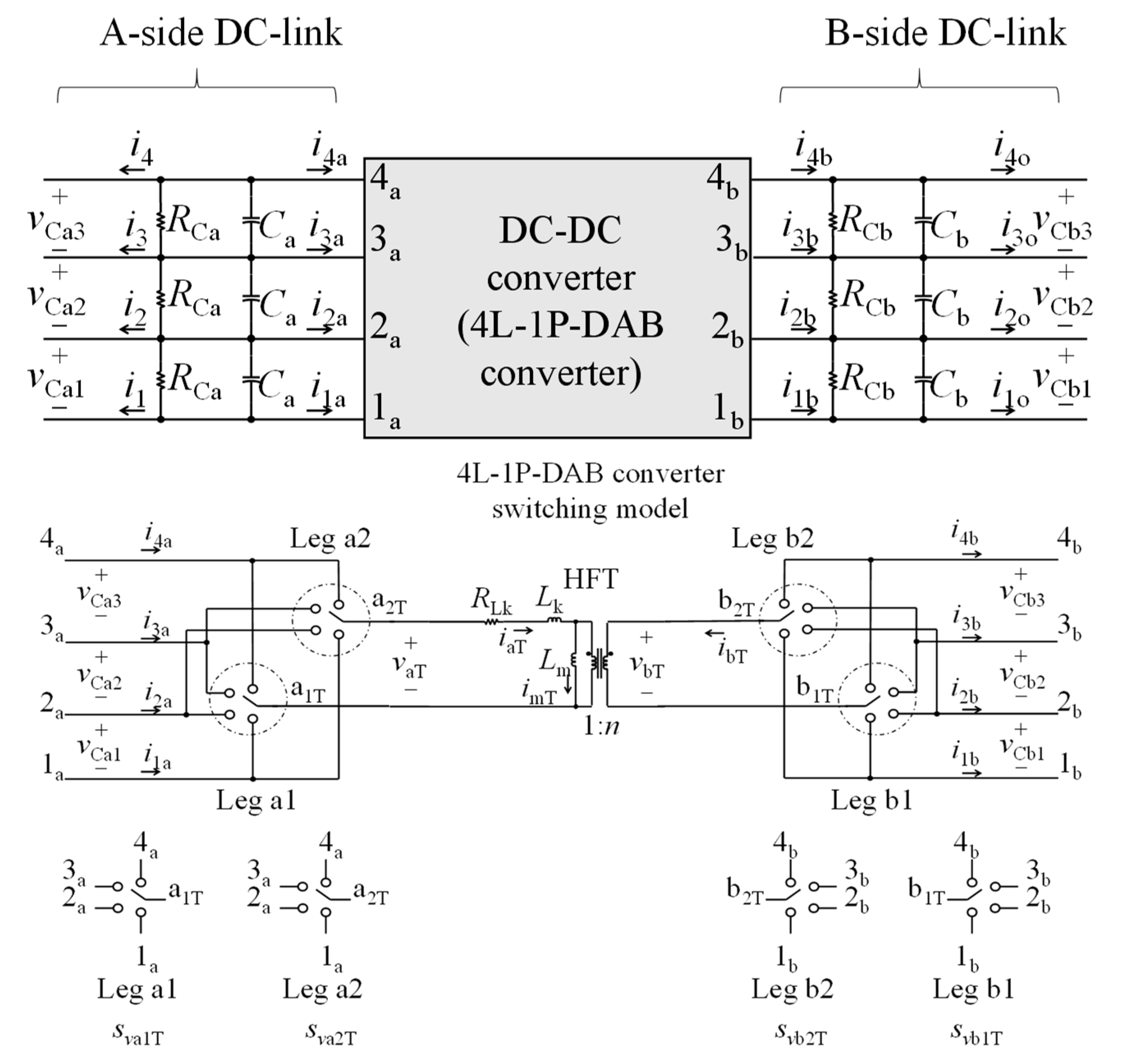
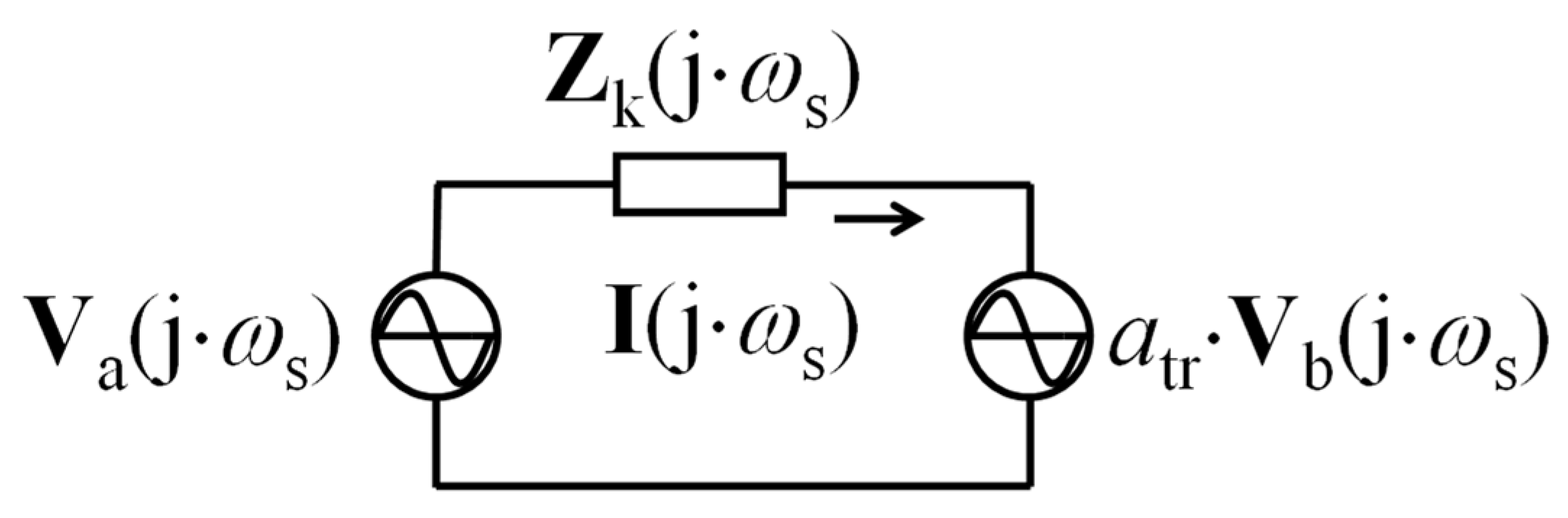
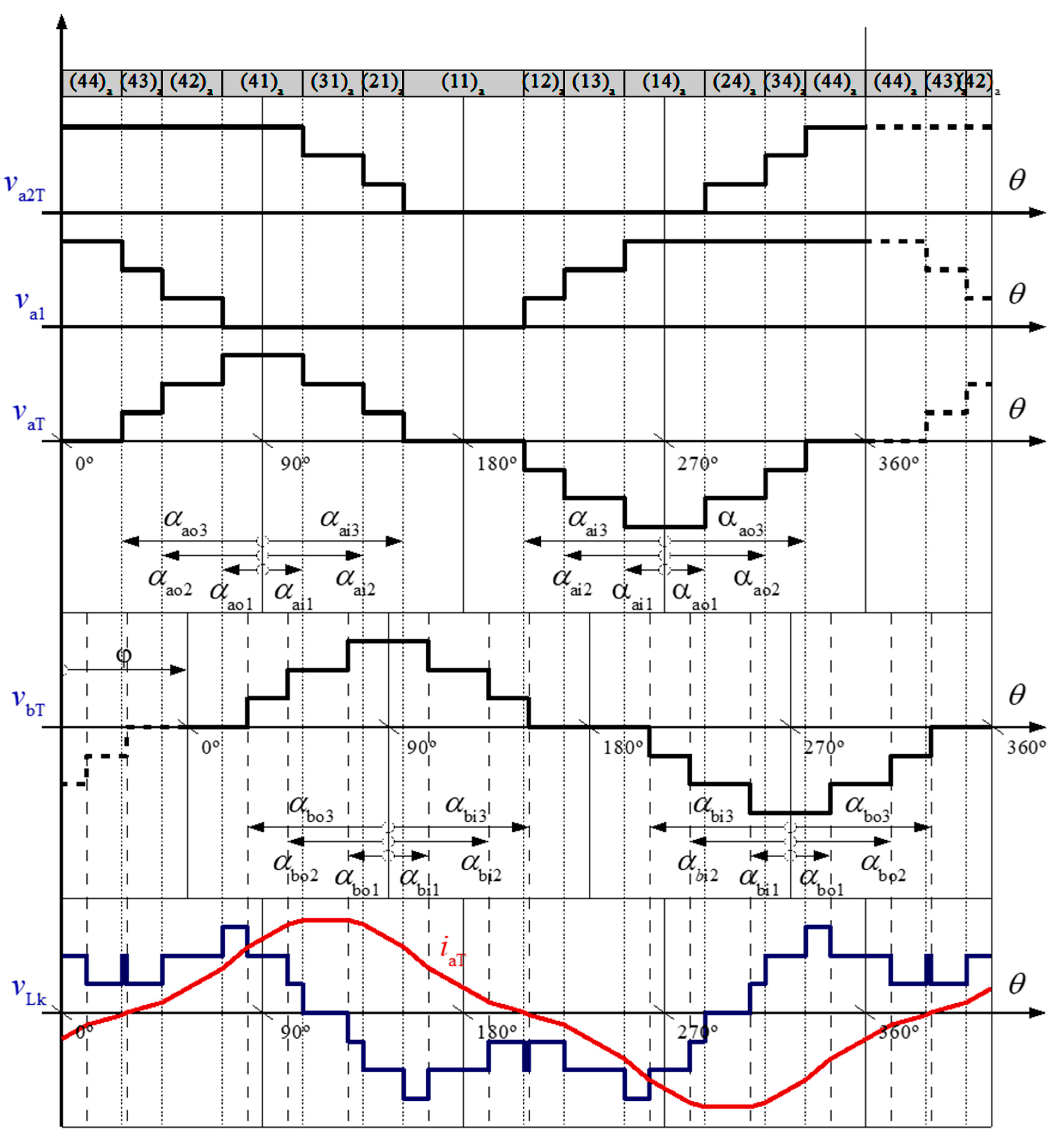
3.2. 4L-1P-DAB Converter Switching Model

Figure 3 provides a comprehensive switching model of the 4L-1P-DAB converter. In this model, the primary and secondary side input currents of the HFT are denoted as iaT and ibT, respectively, and the magnetizing current is represented by imT. The input terminal voltages on the HFT’s primary and secondary sides are labeled as vaT and vbT, respectively. Parameters RLk, Lk, Lm, and atr correspond to the resistance and leakage inductance of the HFT windings, the magnetizing inductance, and the turn ratio (atr = 1/n) of the HFT, respectively. The relationship between leakage and magnetizing inductance is expressed as Lk||Lm = LmLk/Lk + Lm, reflecting the parallel combination in the equivalent circuit.
The b-side DC-link voltages across capacitors are denoted by vCb1, vCb2, and vCb3. The currents through the b-side DC-link, i1b, i2b, i3b, and i4b, correspond to the currents entering the battery bank, while i1o, i2o, i3o, and i4o are the currents directly flowing through the battery bank.
The model also incorporates the capacitors Cb and the bleeding resistors RCb of the b-side DC-link. This switching model describes the dynamic behavior of the 4L-1P-DAB converter, emphasizing its interaction with the battery bank and detailing the complex interplay between converter components and the battery storage system.
Based on the configuration in Figure 3, the switching model of the 4L-1P-DAB converter is presented in the following:
d x 2 d t = A 2 t · x 2 + B 2 · u 2
where x2 = [vCa1, vCa2, vCa3, iaT, imT, ibT, vCa1, vCa2, vCa3]T and u2 = [i2, i3, i4, i20, i30, i40]T. Symbolically, x2 ∈ {ℝ9} and u2 ∈ {ℝ6}. Matrices A2(t) and B2 are defined in Appendix A, as in the case of the 4L-3P-NPC converter. In this converter, the state matrix A2(t) is also time-varying, mainly due to the presence of the switching functions. The corresponding switching functions of the converter are defined as follows:
s v w = 1 ,     v   c o n n e c t e d   to   w 0 ,     else , where v { 1 a ,   2 a ,   3 a ,   4 a ,   1 b ,   2 b 2 ,   3 b ,   4 b ,   } ,   w { a 1 T ,   a 2 T ,   b 1 T ,   b 2 T }
s1aw + s2aw + s3aw + s4aw = 1
s1bw + s2bw + s3bw + s4bw = 1

3.3. Battery Bank Model

The configuration of the battery bank within the 4L-BC system is detailed in Figure 4. The battery bank consists of three battery packs connected to the b-side DC-link, with its mathematical model given by:
d i B d t = R d c L d c · I 3 · i B + 1 L d c · B 3 · v
where iB = [iB1, iB2, iB3]T and v = [vCb1, vCb2, vCb3, vB1, vB2, vB3]T. Symbolically, iB ∈ {ℝ3} and v ∈ {ℝ6}. In addition, I3 is the 3 × 3 identity matrix and B3 is defined in Appendix A. Also, iB1, iB2, and iB3 denote the charging currents, while vB1, vB2, and vB3 represent the terminal voltages of the respective battery packs.
The inductance Ldc and resistance Rdc of the wires affect the transient and steady-state behavior of the system during the charging process. Each battery pack in the bank is modeled using a Thévenin equivalent circuit [29,30], which incorporates a voltage source representing the open-circuit voltage of the battery, indicative of its state of charge.

4. Large-Signal Averaged Model

The large-signal averaged models of the three main components of the 4L-BC system are presented in this section: the 4L-3P-NPC converter, the 4L-1P-DAB converter, and the battery bank. These models help to analyze the dynamic behavior of the 4L-BC system under different operating conditions, providing a macroscopic view by smoothing out high-frequency switching effects and aiding in control algorithm design [32,33].
The 4L-3P-NPC converter model describes the interactions between the AC grid and DC-link, while the 4L-1P-DAB converter model details the HFT operation. The battery bank model accounts for electrochemical characteristics and charge/discharge cycles [27]. These averaged models support developing control strategies to improve efficiency, stability, and energy management.
Classical control theory uses continuous-time representations, requiring an averaging operator to convert discrete switching signals into continuous duty ratios. The averaging operator is defined as follows:
x T s = 1 T s · t T s t x τ d τ
To ensure accurate correlation between actual and averaged values, the switching frequency fs must be significantly higher than the AC grid fundamental frequency fo. In this work, a 10 kHz frequency is used for both converters, which is higher than the 50 Hz grid frequency.
Applying this averaging process enables developing continuous-time models for effective control system design, bridging the gap between the discrete nature of power electronics and the classical control methodologies.

4.1. 4L-3P-NPC Converter Large-Signal Averaged Model

The averaging operator defined in (9) is applied to the switching model of the converter, as detailed in (1). The Park transformation then provides the large-signal averaged model in the D-Q reference frame. The resulting compact differential equation is given by:
d v C a i T s d t = 1 C a · v C a i T s R C a + j i v C a i T s · i 2 T s k = 1 3 v C a k T s + v C a m T s · i 3 T s k = 1 3 v C a k T s + n = 2 4 i n a T s + + v d T s · i d T s + v q T s · i q T s k = 1 3 v C a k T s ,   h e r e i ,   j ,   k 1 , 2 , 3 ,   j i ,   m i j
The resulting model consists of five state variables, ⟨idTs, ⟨iqTs, ⟨vCa1Ts, ⟨vCa2Ts, and ⟨vCa3Ts, and six input variables, ⟨i2Ts, ⟨i3Ts, ⟨i2aTs, ⟨i3aTs, and ⟨i4aTs, plus control variables ⟨vdTs and ⟨vqTs.
Although the model is nonlinear, its variables reach constant values in steady state, making it valuable to analyze the behavior of the 4L-3P-NPC converter and to design proper control strategies.

4.2. 4L-3P-DAB Converter Large-Signal Averaged Model

The derivation of the large-signal averaged model for the 4L-1P-DAB converter begins with establishing a phasor representation as the converter’s fundamental model, based on [20]. Figure 5 presents the sinusoidal steady-state model, focusing solely on the fundamental frequency, equated to the switching frequency fs for simplicity [20,25]. This model considers two phase-shifted sinusoidal AC voltages with amplitudes determined by modulation angles αx1, αx2, and αx3, where x ∈ {a, b}, as detailed below in Section 6.4.
The key circuit parameters are defined as follows:
X L k j · ω s = ω s · L k Z k j · ω s = R L k + j · X L k j · ω s K x = 2 3 · π · cos π 2 α x 1 + cos π 2 α x 2 + cos π 2 α x 3 ,   x a , b V a j · ω s = K a · v d c a θ a V b j · ω s = a t r · K b · v d c b θ a ϕ
The AC voltage amplitudes are expressed as Va(j⋅ωs) = Kavdcaθa and Vb(j⋅ωs) = atrKbvdcb ∠ (θaϕ).
Power transfer at the HFT input PaHFT and output PbHFT is obtained and shown as follows:
P a H F T = R e V a j · ω s · I * j · ω s I * j · ω s = 1 Z k j · ω s · K a · v d c a · sin θ a + σ a t r · K b · v d c b · sin θ a ϕ + σ j · 1 Z k j · ω s · K a · v d c a · sin θ a υ a t r · K b · v d c b · sin θ a ϕ υ σ = tan 1 R L k X L k j · ω s ,       υ = tan 1 X L k j · ω s R L k P a H F T = K a · v d c a Z k j · ω s · K a · v d c a · sin θ a + σ · cos θ a + sin θ a υ · sin θ a a t r · K b · v d c b · sin θ a ϕ + σ · cos θ a + sin θ a ϕ υ · sin θ a
P b H F T = P a H F T + P R L k P R L k = R L k · I j · ω s 2
Considering θa = 0, the maximum input power PaHFTmax can be defined as follows:
P a H F T = K a · V d c a Z k j · ω s 2 · K a · R L k · V d c a a t r · K b · V d c b · Z k j · ω s · sin φ σ
and the achieved phase shift ϕ = π/2 is aligned with the steady-state operation values in [20,25], confirming the validity of the model.
The dynamic large-signal model is obtained by developing the following:
d v C a k T s d t = 1 C a · v C a k T s R C a + j k v C a j T s · i j T s + i j a T s m = 1 3 v C a m T s + p d q + p a H F T m = 1 3 v C a m T s for   j , k { 1,2 , 3 }
d v C b k T s d t = 1 C b · v C b k T s R C b + j k v C b j T s · i j b T s m = 1 3 v C b m T s + p a H F T + p R L k m = 1 3 v C b m T s i B k T s for   j , k { 1,2 , 3 }
These equations relate the AC grid in the D-Q frame with the a-side DC-link and also relate the HFT power terms paHFT and pbHFT to the battery charging currents iB1, iB2, and iB3. This development provides an accurate representation of the large-signal behavior of the converter in steady-state and dynamic operation.

5. Small-Signal Model

The large-signal averaged models for the 4L-BC are established for the 4L-3P-NPC converter in (10) and for the 4L-1P-DAB converter in (15) and (16). Both models are continuous but nonlinear. However, linear control techniques are preferred for simplicity and extensive experience.
To utilize linear control techniques, it is essential to linearize the large-signal averaged models by applying the perturbation technique and Taylor series development around the operating point of the system, as described in [32,34]. The operating points are calculated by setting the time derivatives to zero in (10), (15), and (16), and then substituting all variables with their steady-state expressions (denoted in capital letters). The resulting steady-state model of the 4L-BC is given by:
R a c · I d + ω · L a c · I q E l t l + V d = 0 ω · L a c · I d R a c · I q + V q = 0 1 R C a · V d c a + 2 · V C a 1 + V C a 2 + V C a 3 V d c a · I 2 + I 2 a + V C a 1 V C a 2 + 2 · V C a 3 V d c a · I 3 + I 3 a + 3 · P d q + P a H F T V d c a = 0 1 R C b · V d c b + 2 · V C b 1 + V C b 2 + V C b 3 V d c b · I 2 b + V C b 1 V C b 2 + 2 · V C b 3 V d c b · I 3 b + 3 · P a H F T + P R L k V d c b I B 1 I B 2 I B 3 = 0 R d c · I B 1 + I B 2 + I B 3 + V d c b V B 1 + V B 2 + V B 3 = 0 P a H F T = K a · V d c a Z k j · ω s 2 · K a · R L k · V d c a a t r · K b · V d c b · Z k j · ω s · sin φ σ P d q = I d · V d + I q · V q
The model captures the dynamics of the voltage differences across capacitors Ca and Cb (denoted as vCxy, where x ∈ {a, b} and y ∈ {1, 2, 3}), emphasizing the impact of the currents flowing through the midpoints (neutral points) on the capacitor voltage balance, which will be explored in a later subsection.
To simplify (17), known steady-state variables—including currents Iq, I2, I2a, I3, I3a, I2b, I3b, IB1, IB2, and IB3 and voltages Eltl, VCa1, VCa2, VCa3, VCb1, VCb2, VCb3, VB1, VB2, and VB3—are considered. Additionally, currents Iq and those flowing through the neutral points (I2, I2a, I3, I3a, I2b, and I3b) are assumed to be zero. This leads to obtaining the unknown variables Id, Vd, Vq, and ϕ defined by:
I d = E l t l 2 · R a c 2 P a H F T R a c 1 3 · V d c a 2 R a c · R C a E l t l 2 · R a c V d = E l t l + R a c · I d V q = ω · L a c · I d φ = sin 1 Z k j · ω s · P a H F T a t r · K a · K b · V d c a · V d c b · X L k j · ω s K a · R L k · V d c a a t r · K b · V d c b · X L k j · ω s
From the steady-state variables defined in (18), the linearization process can be applied to obtain the small-signal model of the 4L-BC. The variables denoted with the symbol “^”, and the capital letters represent disturbances and steady-state operating points, respectively.
As a multivariable system, the linear model of the 4L-BC can be represented in state space form as follows:
x ˙ = A · x + B · u y = C · x + D · u
where x is the state vector, u is the input vector, and y is the output vector, defined as:
x = i ^ d , i ^ q , v ^ C a 1 , v ^ C a 2 , v ^ C a 3 , v ^ C b 1 , v ^ C b 2 , v ^ C b 3 , i ^ B 1 , i ^ B 2 , i ^ B 3 T u = E ^ l t l , v ^ d , v ^ q , v ^ B 1 , v ^ B 2 , v ^ B 3 , i ^ 2 , i ^ 2 a , i ^ 3 , i ^ 3 a , i ^ 2 b , i ^ 3 b , ϕ ^ T x = y   where   { x ,   y } { R 11 }   and u { R 13 }
Regarding the assumption x = y, it should be noted that in a state space such (19), x and y are related but not necessarily equivalent. In fact, x represents the state variables of the system, which describe the current state of the system. Instead, the output vector y represents the measurable or observable variables of the system [34,35,36].
The state (A), input (B), output (C), and direct transmission (D) matrices are defined as follows: A = A 11 A 12 A 21 A 22 , B = B 11 B 12 A 21 A 22 , C = I, and D = 0. Also, the submatrices Ajk and Bjk, where {j, k} ∈ {1, 2}, are defined in Appendix A. Symbolically, {A, C} ∈ 11×11 and {B, D} ∈ 11×13. Moreover, the submatrices of A can be defined as A116×6, A126×5, A216×6, and A216×6. The submatrices of B can also be defined as {B11, B21} ∈ 6×6, B126×7, and B225×7 (Appendix A). Finally, I and 0 are the identity and zero matrix, respectively.
Since the model presented in (19) is linear, and considering the aim of designing a control system for the 4L-BC using linear design techniques, the Laplace domain representation of the system model is obtained and shown as follows:
I d s = 1 s + K 1 · K 2 · I q s K 3 · E l t l s V d s I q s = 1 s + K 1 · K 2 · I d s + K 3 · V q s V C a i s = 1 s + K 6 · K 4 · I d s K 5 · I q s + K 7 · j i V C a j s + K 8 · V d C b s K 9 · V d s + + 1 i · K 10 · I 2 s + I 2 a s + 1 i + 1 · K 11 · I 3 s + I 3 a s K 12 · ϕ s for   i , j { 1,2 , 3 } V C b i s = 1 s + K 16 · K 15 · V d C a s K 17 · j i V C b j s K 18 · I B i s + 1 i · K 19 · I 2 b s + 1 i + 1 · K 20 · I 3 b s + K 21 · ϕ s for   i , j { 1,2 , 3 } I B i s = K 24 s + K 25 · V C b i s V B i s for   i { 1,2 , 3 }
assuming zero initial conditions, as outlined in [34,37]. This representation in the Laplace domain facilitates the analysis and design of the control system in the frequency domain. The K-constants in (21) are defined in Appendix A.

6. Control System and Modulation Algorithms

The complete control system for the 4L-BC is illustrated in Figure 6, with key control objectives including battery charging current regulation, a-side DC-link voltage regulation (total and individual capacitor balance), and grid power factor control [23,24,38]. The 4L-3P-NPC converter controller is responsible for managing the total a-side DC-link voltage (vdca), controlling reactive power exchange with the grid (ensuring power factor correction), and balancing the a-side DC-link capacitor voltages (vCa1, vCa2, and vCa3) [27,28]. Meanwhile, the 4L-1P-DAB converter controller regulates the battery charging currents (iB1, iB2, and iB3) and can also contribute to a-side DC-link capacitor voltage balancing [25,27]. This dual capability allows a-side DC-link voltage balancing to be achieved using the 4L-3P-NPC converter, the 4L-1P-DAB converter, or both simultaneously, as demonstrated in the three-level battery charger (3L-BC) [23,24]. This flexibility enables user customization based on specific performance and operational requirements.
The mathematical models describing the dynamic open-loop plants of the system are not covered exhaustively in this article. However, a detailed description of these models can be found in [38].
Modulation algorithms play a pivotal role in the operation of the proposed 4L-BC. For the 4L-3P-NPC converter, a virtual-vector pulsewidth modulation (VVPWM) strategy is employed, which enhances voltage balancing, reduces total harmonic distortion, and optimizes switching losses [28]. For the 4L-1P-DAB converter, a four-level extension of the modulation approach defined in [24] is utilized. This strategy involves dynamically adjusting the switching angles to create an optimized voltage waveform for both the primary and secondary sides of the HFT [25]. This modulation not only improves energy transfer efficiency but also ensures precise control over the charging currents of batteries with varying SoC.
By integrating these advanced modulation algorithms into the control architecture, the 4L-BC achieves superior performance in terms of efficiency, flexibility, and reliability.

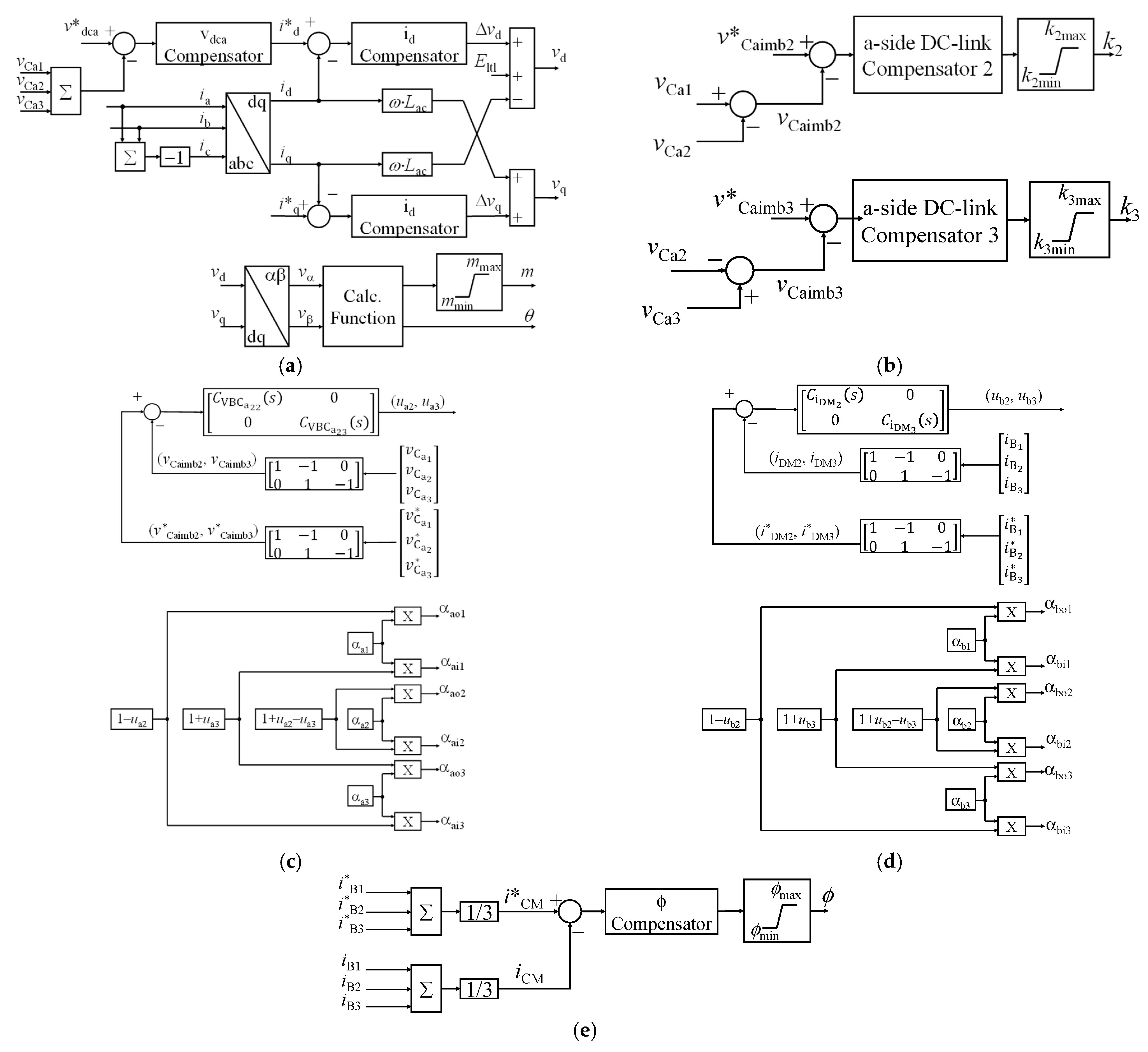
6.1. 4L-3P-NPC Converter Control Description

In this 4L-BC, the voltage-oriented control system is similar to the 3L-BC [23,24,38], but with an additional voltage level. The control system scheme is shown in Figure 7a.
The total a-side DC-link voltage (vdca) is regulated by a PI controller (vdca-compensator), which provides the reference for the D-component of the grid current (id) regulated by another PI controller (id-compensator). The Q-component of the grid current (iq) is regulated by a PI controller (iq-compensator) to control the reactive power flow and maintain a unity power factor. The current controllers generate the vd and vq signals, which are then transformed into α-β variables to obtain the modulation index m = sqrt(vα + vβ) and the reference angle θ = atan(vβ/vα) through a calculation function block (calc. function).
For a-side DC-link voltage balancing, the a-side DC-link compensator (VBCa1) is implemented (Figure 7b). Since the DC-link has three capacitors, there are two voltage unbalances to regulate, vCaimb2 = vCa1vCa2 and vCaimb3 = vCa2vCa3. The implementation includes two compensators, a-side DC-link compensators 2 and 3, which generate control signals (k2 and k3) to reduce the unbalances to zero.
The control system consists of five compensators, namely the two current compensators (id, iq), the a-side DC-link total voltage compensator (vdca), and the two voltage unbalance compensators (vCaimb2 and vCaimb3).

6.2. 4L-3P-NPC Converter Modulation

VVPWM is based on a set of space vectors in the space-vector diagram, called virtual vectors, which are defined as a linear combination of certain switching states [39]. Each virtual vector involves an average zero neutral-point current in every switching cycle. In this way, if the reference voltage vector is synthesized with these virtual vectors, the balance of the voltages of the DC-link capacitors will be guaranteed in each switching cycle [26,40]. This modulation is suitable for this four-level converter and can be implemented as follows:
m o d a θ = 2 3 · m · c o s θ m o d b ( θ ) = 2 3 · m · c o s θ 2 · π 3 m o d c θ = 2 3 · m · c o s θ + 2 · π 3
m o d m a x   θ = max m o d a , m o d b , m o d c m o d m i n   θ = min   m o d a , m o d b , m o d c
d x 1 θ = 1 2 · m o d m a x m o d x d x 2 θ = d x 3 θ d x 3 θ = 1 2 · 1 d x 1 θ d x 4 θ d x 4 θ =   1 2 · d x 1 θ m o d m i n
m = m 1 + k 2 · v C a 3 + v C a 2 v C a 1 v d c a + k 3 · v C a 3 v C a 2 v C a 1 v d c a r = m m = 1 1 + k 2 · v C a 3 + v C a 2 v C a 1 v d c a + k 3 · v C a 3 v C a 2 v C a 1 v d c a
d x 1 θ = d x 1 · 1 k 2 k 3 · r d x 2 θ = d x 2 · + k 2 · d x 1 d x 4 d x 3 θ = d x 3 · + k 3 · d x 1 d x 4 d x 4 θ = d x 4 · 1 + k 2 + k 3 · r
where x ∈ {a, b, c} [28].
In (24), the basic form of the leg duty ratios is calculated, without considering the control action determined by the closed-loop capacitor voltage balancing control. While the modulation strategy aims to achieve capacitor voltage balance in all operating conditions, non-idealities in the converter can still cause slight capacitor voltage unbalance.
Therefore, the closed-loop capacitor voltage balance control shown in Figure 7b becomes necessary. The closed-loop control in Figure 7b generates control parameters k2 and k3, which modify the values of the open-loop leg duty cycles given in (26). This modification is required to ensure proper capacitor voltage balancing in the presence of converter non-idealities.
The correction factor r defined in (25) is necessary to prevent the capacitor voltage balancing action from perturbing the intended m value when the DC-link capacitor voltages are different. It ensures that the voltage balancing control does not affect the desired m, maintaining converter performance and stability.

6.3. 4L-1P-DAB Converter Control Description

The control schemes for the 4L-1P-DAB are shown in Figure 7c–e [25,27]. The 4L-1P-DAB converter has the capability to regulate the imbalance of the voltages vCa1, vCa2, and vCa3 (VBCa2) similar to the 3L-3P-NPC converter (VBCa1) [23,24,38]. The control efforts ua2 and ua3 are produced to achieve a zero imbalance, i.e., vCaimb2 = vCa1vCa2 and vCaimb3 = vCa2vCa3, controlling the necessary switching angles αaxy where x ∈ {o, i} and y ∈ {1, 2, 3} [25].
In addition, the 4L-1P-DAB converter regulates the battery pack charging currents iB1, iB2, and iB3 by controlling the differential-mode (DM) and common-mode (CM) components, i.e., iDM2 = iB1iB2, iDM3 = iB2iB3, and iCM = (iB1 + iB2 + iB3)/3 [27]. The control efforts ub2 and ub3 produce the necessary switching angles αbxy, where x ∈ {o, i} and y ∈ {1, 2, 3}, for the proper operation of the modulator of the 4L-1P-DAB converter (Figure 7d).
Figure 7e shows the control diagram for iCM control, where the power transfer of the 4L-1P-DAB converter is regulated by controlling the phase angle ϕ [27].
The control system associated with the 4L-1P-DAB converter is constituted by five PI compensators, the detailed development of which can be found in [38].

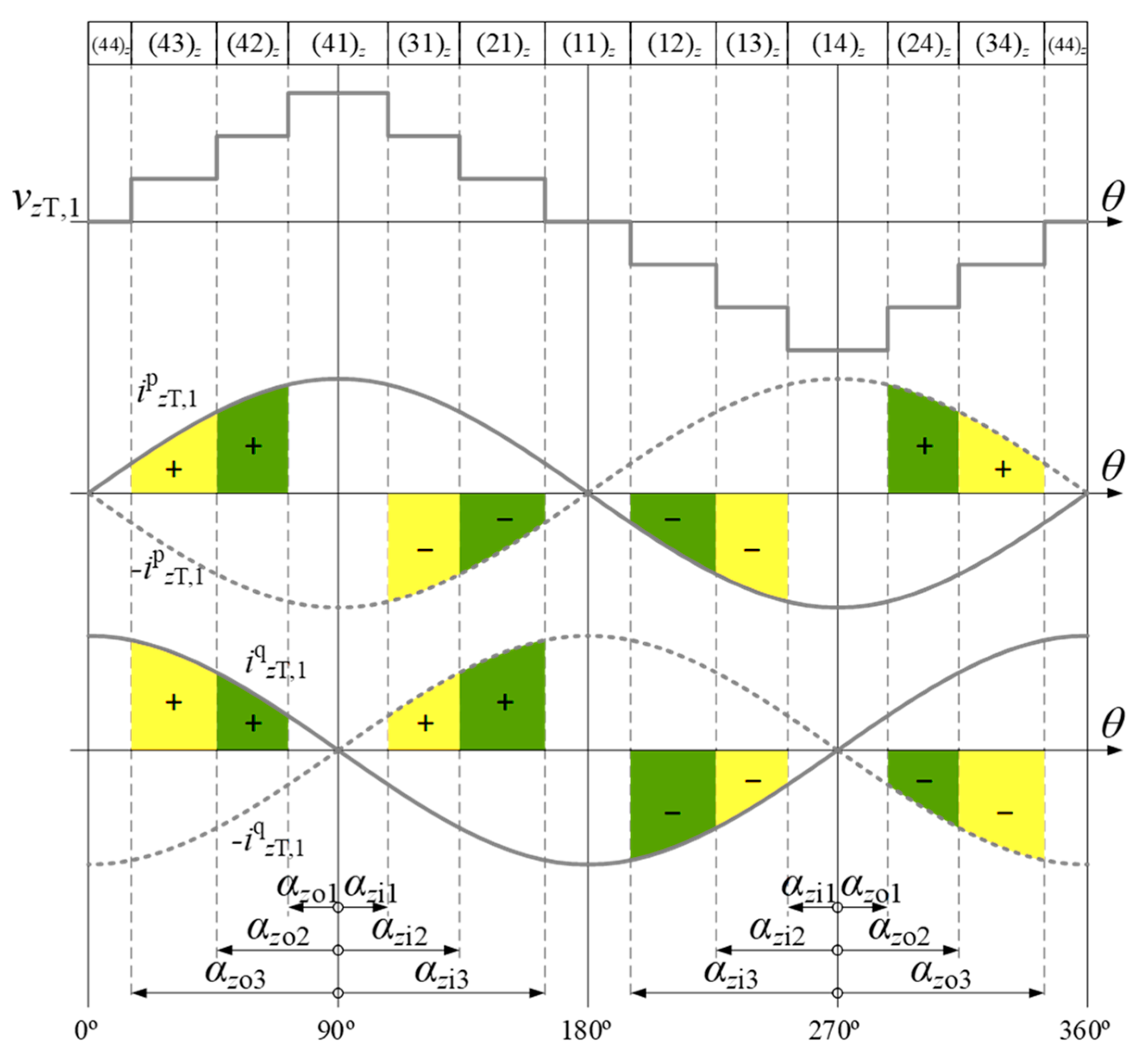
6.4. 4L-1P-DAB Converter Modulation

The switching strategy for this four-level converter, as shown in Figure 8, is based on modifying the switching angles to achieve a specific shape of the voltages on the primary and secondary sides of the HFT [25]. Figure 8 illustrates the waveforms of the voltages on the primary (vaT) and secondary (vbT) sides of the HFT, the voltage across inductance Lk (vLk), and the current flowing through the a-side of the HFT (iaT). Moreover, this modulation strategy aims to build seven levels in the voltages vaT and vbT. The power transfer between the a- and b-side of the converter is regulated through the phase-shift angle ϕ and the switching angles αzjk, where z ∈ {a, b}, j ∈ {i, o}, and k ∈ {1, 2, 3}.
It is worth mentioning that for z ∈ {a, b}, vzT exhibits a predetermined switching state sequence as depicted in the top Figure 8.
The six switching angles per side (αzi1, αzi2, αzi3, αzo1, αzo2, and αzo3) plus the ϕ sum up 13 degrees-of-freedom available to control capacitor voltage balancing, converter performance, and power flow. If αz1 = αzo1 = αzi1z, αz2 = αzo2 = αzi2z, and αz3 = αzo3 = αzi3z, and the DC-link capacitor voltages are balanced, then quarter-wave symmetry is guaranteed and even order harmonics are eliminated in vaT, vbT, vLk, and iaT waveforms [25].
The operating principle of this modulation involves drawing or injecting current from the two neutral points of the a- and b-side DC-link (i2z and i3z, where z ∈ {a, b}) to balance the voltages vCax and vCbx, where x ∈ {1, 2, 3}. That is, vCa1 = vCa2 = vCa3 and vCb1 = vCb2 = vCb3 [25]. The currents i2z and i3z are defined as follows:
i 2 z = s 2 z z 1 T s 2 z z 2 T · i z T i 3 z = s 3 z z 1 T s 3 z z 2 T · i z T
based on the switching model of the 4L-1P-DAB converter, i.e., Equation (4).
To maintain the balance of the a- and b-side DC-link voltages, the total charge injected into the neutral points in a switching cycle must be zero [25]. To simplify the analysis, it is convenient to consider only the fundamental component of izT, i.e., izT,1, as its amplitude is larger than the harmonic amplitudes and is the main contributor to i2z and i3z. Moreover, as shown in Figure 9, izT,1 can be decomposed into the in-phase and in-quadrature components with respect to vzT,1 (the fundamental component of vzT, where z ∈ {a, b}).
To study the dynamics of the charge injection at the neutral points, the effects of the fundamental component of izT, denoted as izT,1, are explored. As its amplitude is larger than the harmonic amplitudes, the effect of the harmonics on the capacitor voltages can be neglected. According to [22,25] and Figure 6 and Figure 7, izT,1 can be decoupled into a component in phase and a component in quadrature with vzT,1 (fundamental component of vzT), as mentioned before, denoted as ipzT,1 and iqzT,1, respectively. The voltage and current vzT,1 and izT,1 are defined by [22,25]:
v z T , 1 = V z T , 1 · sin θ i z T , 1 = i z T , 1 p + i z T , 1 q = I z T , 1 p · sin θ + I z T , 1 q · cos θ
Also, Figure 9 plots the voltage vzT and the currents ipzT,1 and iqzT,1 as a function of θz (the phase angle of vzT,1). The green- and yellow-shaded areas represent the electric charges injected toward (positive sign) and drawn from (negative sign) the DC-link neutral points 2z and 3z, respectively. These charges are provided by the currents ipzT,1 and iqzT,1. To keep a preexisting capacitor voltage balance, the sum of the yellow areas must be zero and the sum of the green areas must also be zero. This is accomplished if the following is satisfied:
sin(αz1) + sin(αz3) − 2·sin(αz2) = 0
However, even when (29) is satisfied, converter non-idealities may lead to non-zero average neutral-point currents causing capacitor voltage unbalances. Any voltage imbalance in vCax and vCbx, where x ∈ {1, 2, 3}, can be corrected by modifying switching angles αzjk (where z ∈ {a, b}, j ∈ {i, o}, and k ∈ {1, 2, 3}) in order to inject or draw charge within a switching period. Note that this electric charge is only supplied by ipz_HFT,1, since the total charge injected by iqz_HFT,1 is zero due to the odd symmetry of vzT [25,40].

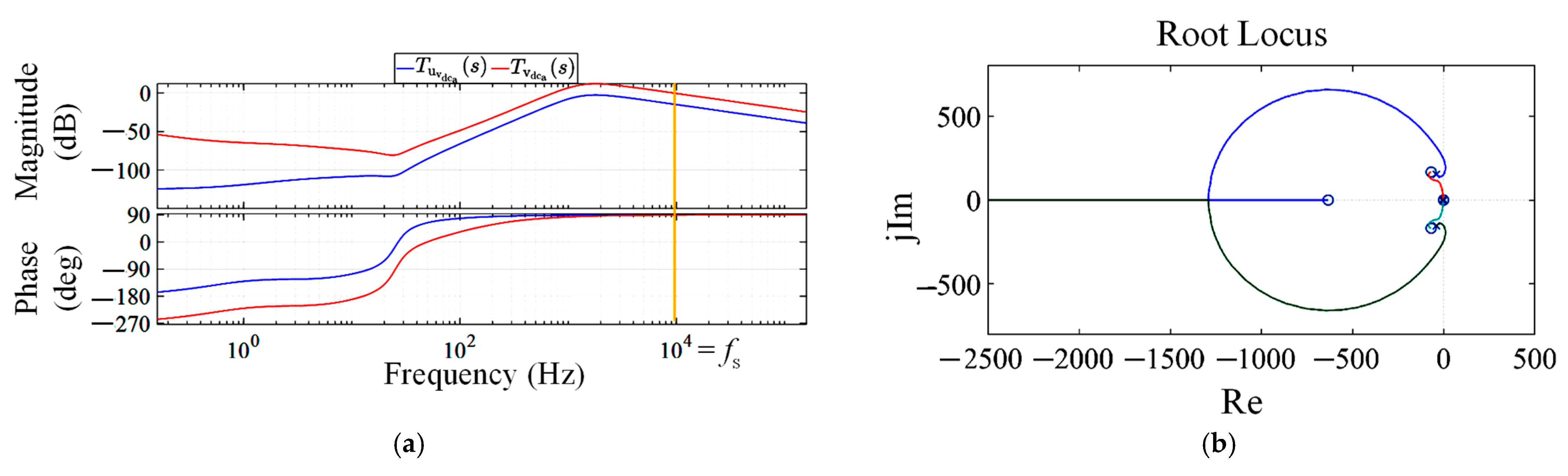
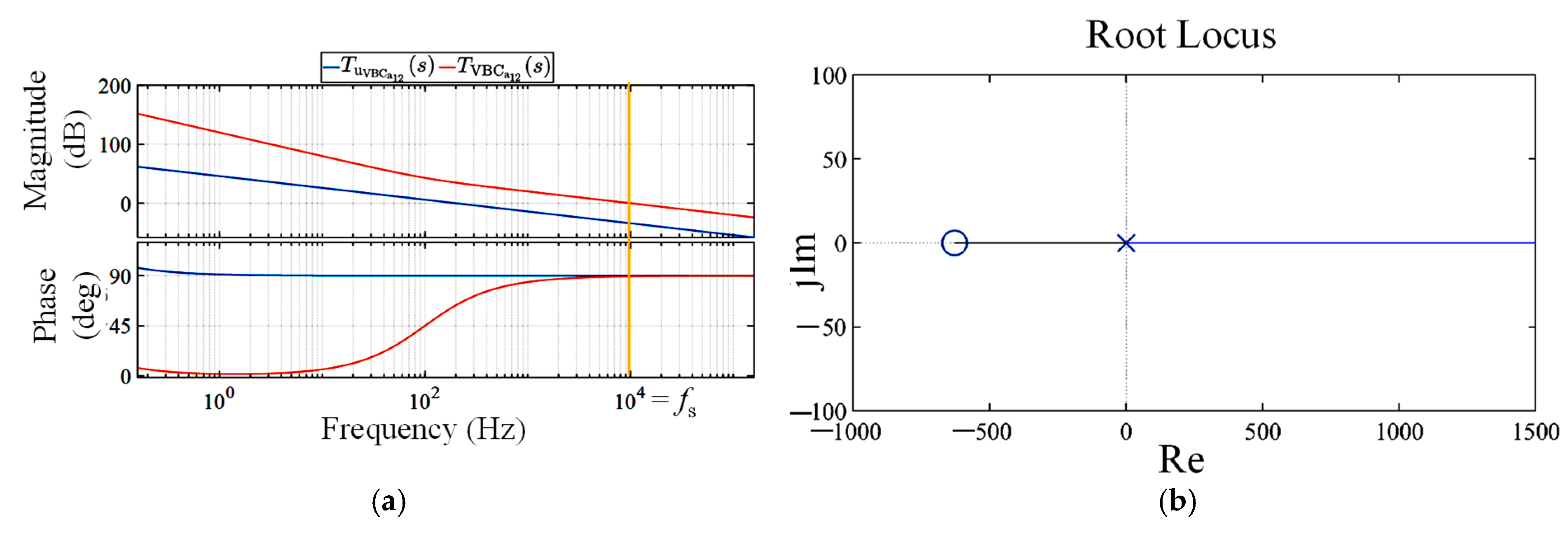
6.5. Control System Transfer Function

The system modeling is described in Section 3, Section 4 and Section 5. This modeling procedure resulted in the linear Equation (21) that describes the behavior of the system. Considering model (21) and the control system schemes described in the previous subsections, the control system transfer functions (TFs) that characterize the dynamics of the closed-loop system can be obtained. This section provides a theoretical analysis of these TFs.
As previously introduced, the 4L-BC is composed of a cascaded configuration integrating a 4L-3P-NPC and a 4L-1P-DAB. Each converter operates under a dedicated multiloop control framework designed to meet specific objectives such as DC-link voltage regulation, grid current tracking, voltage balancing, and controlled power flow. It is worth noting that the averaged and linearized models of the system obtained from the modeling procedure were used to tune the controllers. The explicit mathematical expressions of the TFs are detailed in Appendix A, and the controller design methodology used in this work is described in [38].

6.5.1. Voltage Regulation Loop—4L-3P-NPC

The outer voltage regulation loop of the 4L-3P-NPC converter governs the total a-side DC-link voltage, denoted as vdca. The associated transfer function, representing the plant to be controlled, is given by:
G v d c a s = V d C a s I d s Y s = 0
This TF (see Appendix A) describes the interactions between the AC-side grid current Id, the DC-link capacitors Ca, resistive losses RCa, and the interconnection impedance ∣Zk(jωs)∣ influenced by the DAB stage. It results in a high-order coupled system that includes both fast-switching and low-frequency dynamics. The pole-zero distribution of this TF is nontrivial, featuring multiple dominant poles associated with energy storage elements and parasitic resistances. This complexity requires careful controller design to achieve stability and bandwidth objectives.

6.5.2. DQ-Frame Current Regulation Loops

The inner loops of the 4L-3P-NPC converter regulate the d- and q-axis components of the grid current. These currents are crucial for enforcing grid-side power factor correction and establishing reference-tracking behavior. Both axes are governed by a shared second-order plant model, expressed as:
G d s = G q s = G d q s = I d s V d s = I q s V q s
(refer to Appendix A). This TF encapsulates the behavior of the LC filter and its interaction with the grid impedance. The zero at s = −ξωn enhances phase response, allowing for higher control bandwidth while maintaining a sufficiently large phase margin. The pole placement is linked to the natural frequency ωn and damping ratio ξ, both of which are functions of Rac and Lac. These loops serve as the backbone for the voltage control loop, providing a fast dynamic response necessary to maintain tight regulation under transient disturbances.

6.5.3. A-Side DC-Link Voltage Balancing

The three a-side DC-link capacitors may exhibit voltage imbalances due to asymmetries in load or converter operation. Two dedicated loops are implemented to actively balance the voltages by controlling the imbalance terms:
v C a i m b 2 = v C a 1 0.5 · v C a 2 + v C a 3 v C a i m b 3 = 0.5 · v C a 1 + v C a 2 v C a 3
The corresponding plant dynamics are governed by first-order TFs:
G C a i m b k s = V C a i m b k s I k s
where k ∈ {2, 3} (see Appendix A). These functions reflect the RC-like dynamics of charge balancing among the capacitor banks. Dominant poles are determined by the product RCaCa, and the system is inherently stable. However, due to their low-pass nature, these loops must be carefully compensated to prevent slow behavior or excessive control action during large transients [41].

6.5.4. Differential-Mode Current Control—4L-1P-DAB

The DM current control loops are designed to regulate the charging current imbalance across the individual battery packs. These loops act on the differential currents:
i D M 2 = i B 1 i B 2 i D M 3 = i B 2 i B 3
The associated plant TFs are modeled as second-order systems:
G C i m b k s = I D M k s I k b s
where k ∈ {2, 3} (see Appendix A). These TFs include poles determined by the coupled dynamics of the DAB converter modulation index, interlink inductance Lk, and battery pack voltages. Resonant behavior may arise depending on pole locations, and loop gain compensation must account for potential peaking in frequency response.

6.5.5. Common-Mode Current Control and Power Transfer

The net power transfer from the AC-side grid to the battery bank is controlled through the regulation of the common-mode current component defined by:
i C M = 1 3 · j = 1 3 i B j
The plant TF associated with this loop is modeled as shown as follows:
G ϕ s = I C M s ϕ s
which is defined in Appendix A.
The presence of a right-half-plane zero at s = −ωz introduces a non-minimum phase characteristic, imposing a theoretical upper limit on control bandwidth. The cubic denominator includes dominant low-frequency poles resulting from interactions between converter inductance, DC-link dynamics, and modulation phase angle ϕ. The sensitivity of this loop to parameter variations and input disturbances requires conservative tuning strategies, especially in systems where rapid power fluctuations may occur.

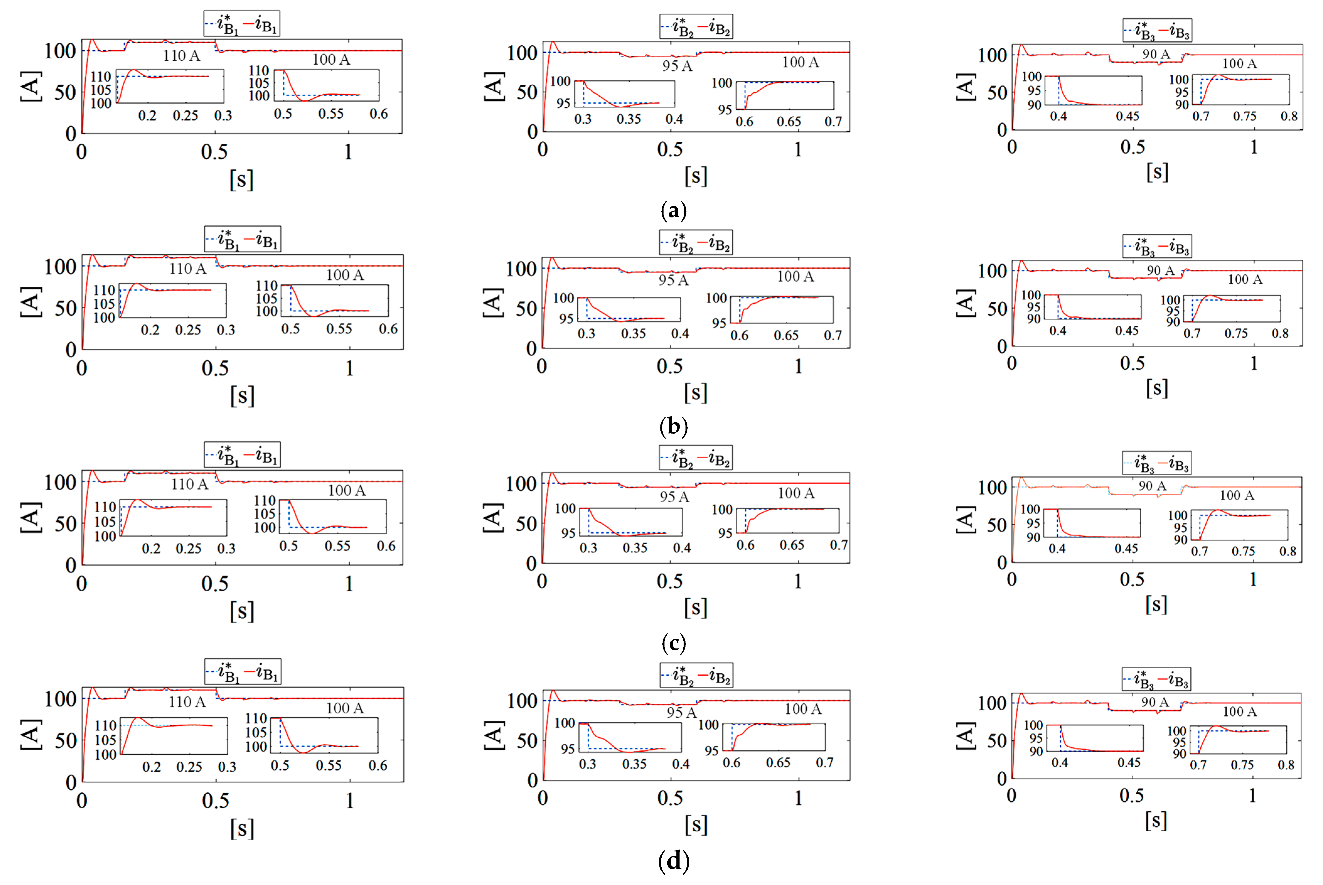
7. Simulation Results

7.1. Specifications, Scenarios, and Cases Definition

Simulations were carried out with the model shown in Figure 1, using MATLAB/Simulink, version R2019b. The 4L-BC was connected to a three-phase AC grid with Eltl_ss = 400 Vrms line-to-line and f = 50 Hz. Both converters in the 4L-BC operated with a switching frequency fs = 10 kHz.
The converter parameter values are listed in Table 1. The initial a-side DC-link capacitor voltages are vCa10 = 280 V, vCa20 = 420 V, and vCa30 = 700 V; i.e., the system starts with the a-side DC-link with its voltages imbalanced. The a-side DC-link voltage reference is set at v*dca = 1.4 kV. The initial voltages of the b-side DC-link capacitors vCb10, vCb20, and vCb30 are imposed by the voltages of each battery pack vB1, vB2, and vB3. Charging current references i*B1, i*B2, and i*B3 are set to 100 A. The switching angles are initially defined as follows: αz1 = 10°, αz2 = 35.4°, and αz3 = 80°, where z ∈ {a, b}, which are consistent with (29) and thus force ipzT,1 to deliver a zero charge to the inner DC-link points [22,25].
Four different scenarios are generated for this 4L-BC according to four different capacitance ratings of the a-side DC-link capacitors, as shown in Table 2.
Similarly to the analysis for the 3L-BC case performed in [24], the characteristics and performance under each scenario are studied in the same three cases that were defined in the 3L-BC. As shown in Table 3, these cases are defined depending on the converters in charge of balancing the a-side DC-link, that is, to keep vCa1, vCa2, and vCa3 balanced.

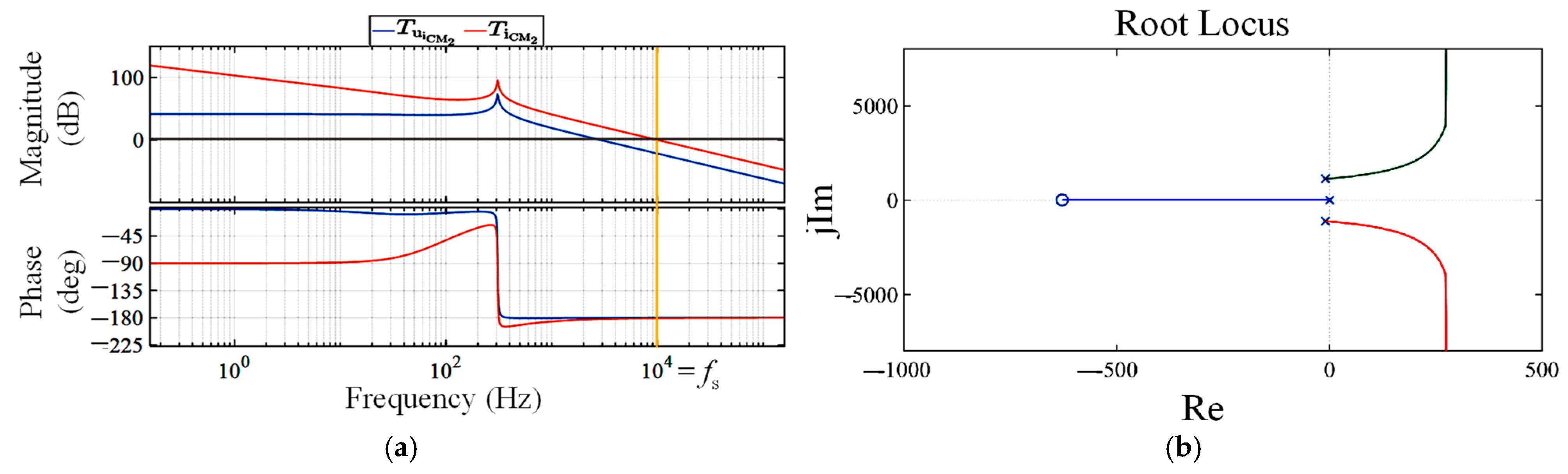
7.2. System Stability Analysis

As detailed in previous sections, the linear model of the system was used to tune the controllers described in Section 6, as documented in [38]. A detailed frequency-domain stability analysis was carried out for all closed-loop systems in the 4L-BC architecture. Each control loop—covering DC-link voltage, DQ-frame current, voltage balancing, DM, and CM components—was subjected to classical loop-gain analysis using Bode plot evaluation and root locus inspection. As described in [38], the crossover frequency of each compensated open-loop transfer function was tuned to match the converter switching frequency fs = 10 kHz, ensuring minimal phase lag, high disturbance rejection, and fast transient response.
Figure 10a shows that the uncompensated open-loop gain Tvdcau(s) of the 4L-3P-NPC converter outer voltage loop lacks a crossover near fs. However, after compensator insertion, the resulting loop gain Tvdca(s) exhibits a crossover precisely at fs with a substantial phase margin of 270°, confirming stability and responsiveness. The corresponding root locus diagram in Figure 10b reveals all poles confined to the left-half complex plane, further validating system stability.
Similarly, the DQ-frame current controllers—governing Gdq(s)—show uncompensated crossover points at 30 Hz and 102 Hz (Figure 11a, blue). After compensation, the gain crossover shifts toward fs, with a phase margin of 86° (Figure 11a, red). The root locus plot in Figure 11b confirms left-half-plane pole placement, affirming robust current control.
The voltage balancing loops CVBCa12(s) and CVBCa13(s), governing imbalances vCaimb2 and vCaimb3, also exhibit crossover frequencies at fs with phase margins exceeding 270°, as seen in Figure 12a,b. This implies the excellent dynamic suppression of capacitor voltage
On the 4L-1P-DAB side, Figure 13 and Figure 14 reveal that the DM current controllers, TiDM2(s) and TiDM3(s), are very stable, exceeding 360° of phase margin. This high phase margin is attributed to the inherent second-order plant dynamics and well-tuned compensators.
Finally, the most demanding control loop—the common-mode current controller regulating iCM through phase angle ϕ—is analyzed in Figure 15. Despite the non-minimum phase behavior of Gϕ(s), the compensated loop Tϕ(s) achieves a robust phase margin of 258°, with root locus analysis verifying strict left-half-plane pole locations.
In conclusion, all control loops within the 4L-BC system—whether linear or nonlinear, single-input or multiple-input multiple-output—are well compensated, phase-stable, and dynamically resilient. These results validate the theoretical modeling presented in Section 6.5 and demonstrate the practical effectiveness of the control architecture under both steady-state and dynamic operating conditions.

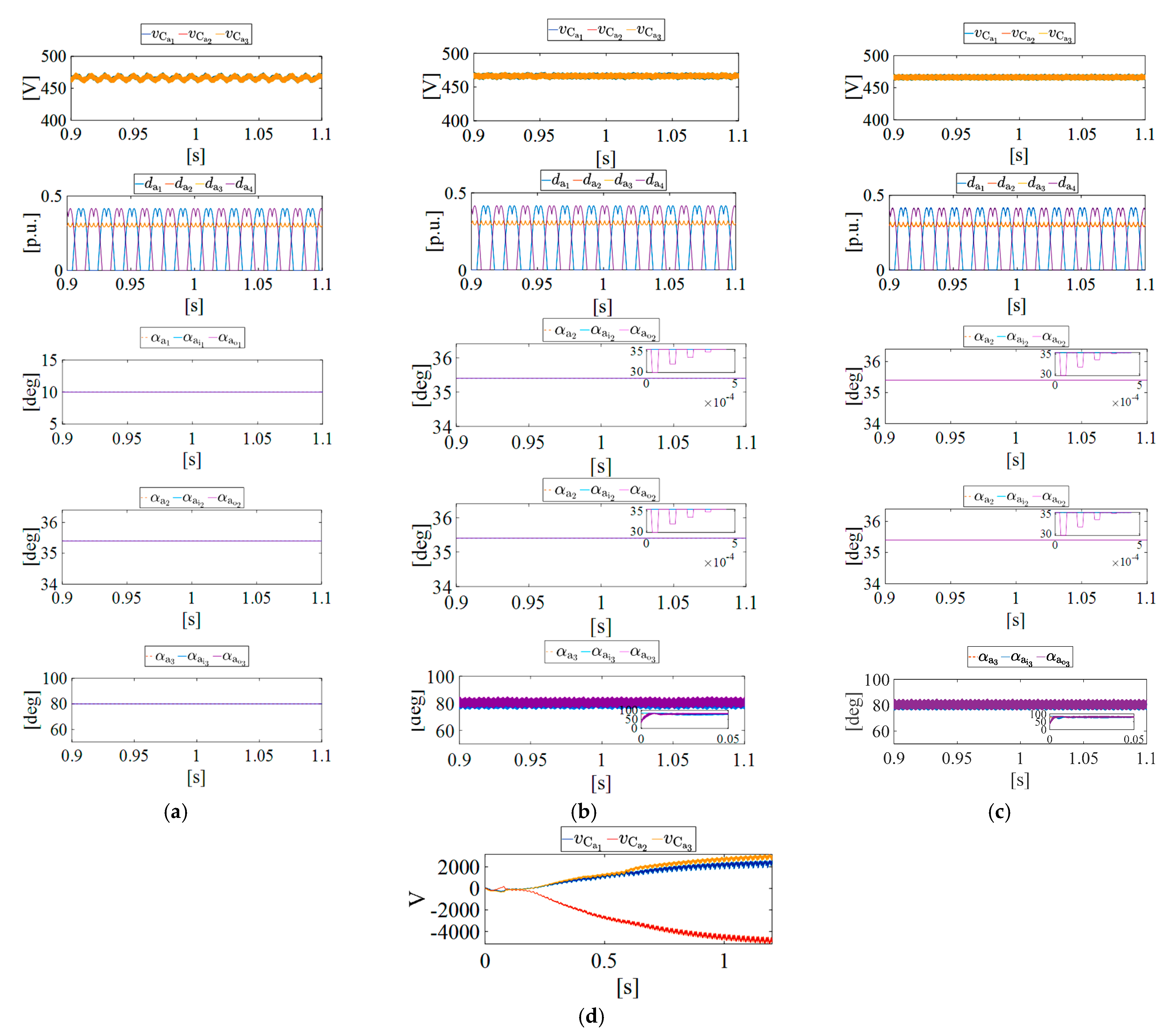
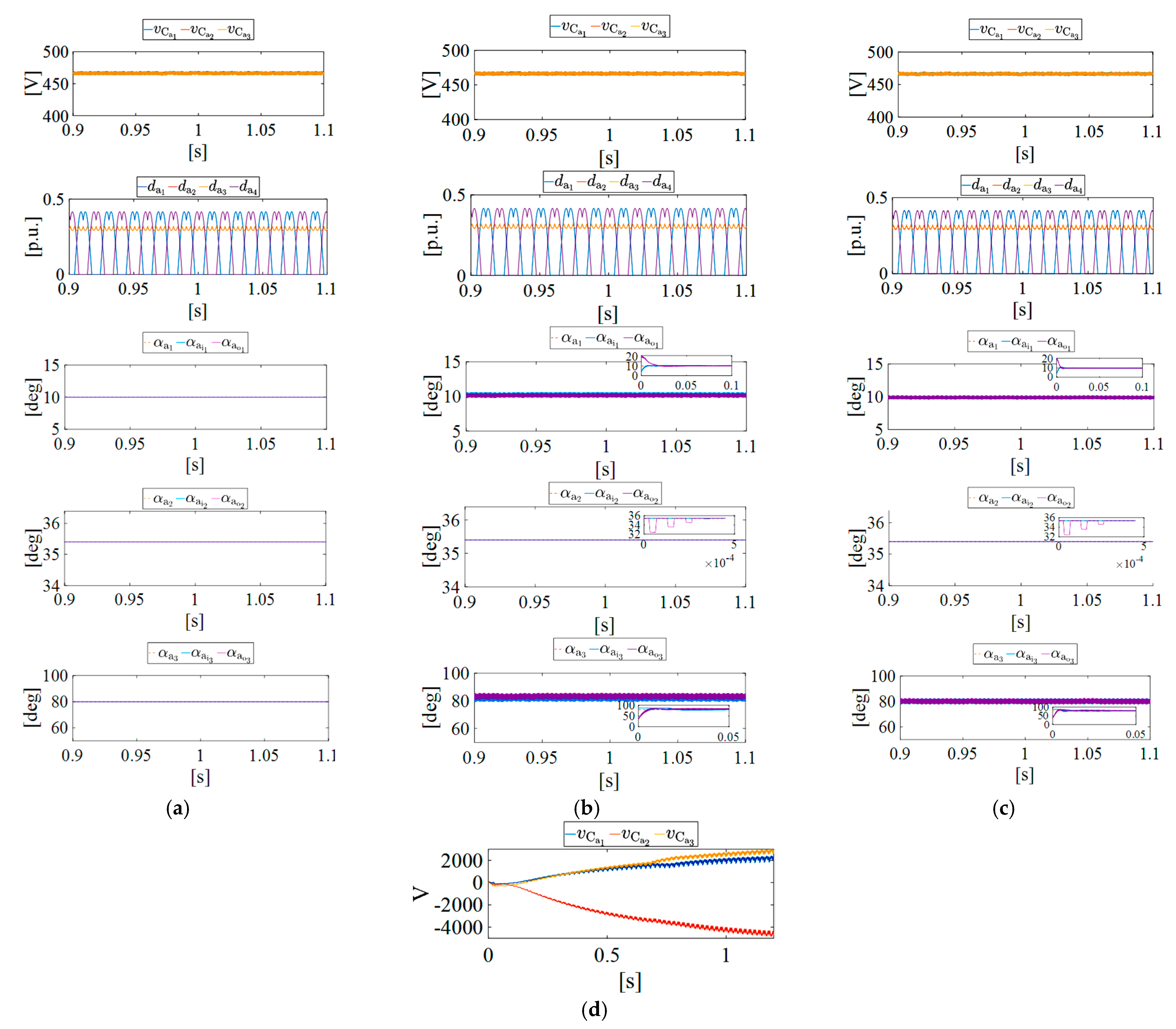
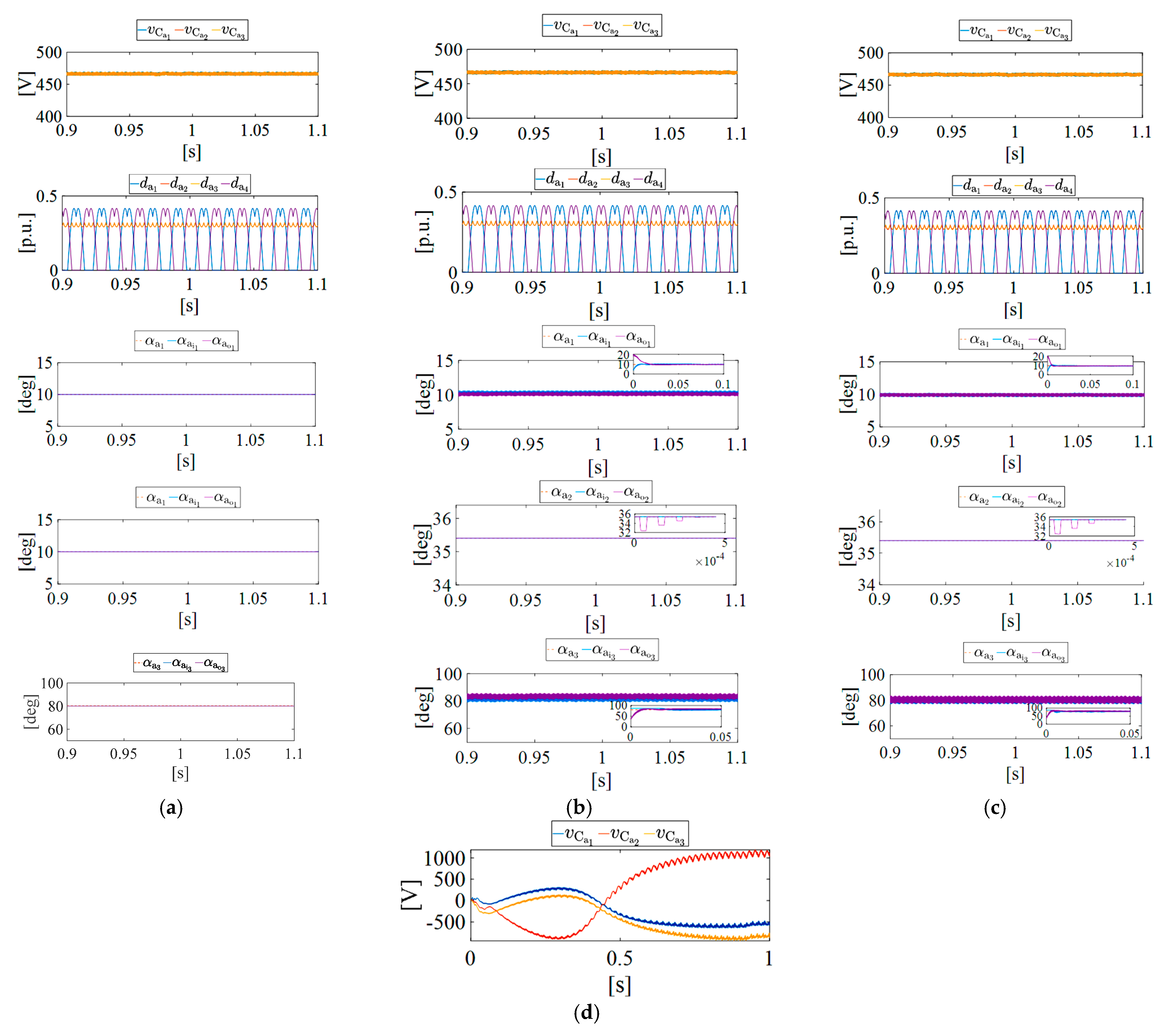
7.3. Time-Domain Simulation Results

In this subsection, the time-domain simulation results are presented for the proposed simulation scenarios and cases.
Figure 16, Figure 17, Figure 18 and Figure 19 depict the value of voltages vCa1, vCa2, and vCa3, leg “a” duty ratios da1, da2, da3, and da4, and switching angles corresponding to side a, i.e., αajk where j ∈ {i, o} and k ∈ {1, 2, 3}, with the system in steady-state operation, for scenarios 1 to 4, respectively. Figure 16a–c, Figure 17a–c, Figure 18a–c, 19a–c correspond to cases 1 to 3, respectively. Additionally, Figure 16d, Figure 17d, Figure 18d, Figure 19d shows the dynamics of the voltages vCa1, vCa2, and vCa3 in the absence of balance control of these voltages.
It is worth highlighting that the a-side DC-link voltage balance is essential for proper system operation. The first row in Figure 16, Figure 17, Figure 18 and Figure 19 shows balanced a-side DC-link voltages in all conditions. To demonstrate the effectiveness of the balance control loop, the simulations in Figure 16d, Figure 17d, Figure 18d, Figure 19d were carried out with this control deactivated. Without balance control, the a-side DC-link voltages become unbalanced and reach unsafe values, which necessarily leads to a system shutdown to avoid system damage. It should be noted that the negative DC-link voltages shown in the simulation results would not be possible in a real system, since they will be clamped at zero by the converter diodes. Overall, it is obvious that the voltage balancing control loop is essential.
Under proper balanced operation, the high-frequency ripple observed in vCa1, vCa2, and vCa3 (first row in Figure 16, Figure 17, Figure 18 and Figure 19) decreases with increasing capacitance from scenario 1 to 4, reflecting the filtering characteristics of the DC-link. In high-performance charging systems, a ripple threshold of 1.5% is typically enforced, guiding the DC-link capacitor design for both energy storage and dynamic filtering.
A figure of merit (FoM) related to the values of the percentage of ripple in the DC-link voltages (rrvca1, rrvca2, and rrvca3) are calculated and summarized in Table 4. Figure 16, Figure 17, Figure 18 and Figure 19 confirm that this requirement is not satisfied in scenario 1 except for vCa2 in case 2, as detailed in Table 4. The ripple performance improves substantially in scenarios 3 and 4, meeting specifications across all cases. The peak ripple is observed in rrvCa1 for scenario 1, case 3, whereas the lowest ripple appears in rrvCa2 for scenario 4.
The duty ratios of the AC-DC converter legs do not reach saturation under any scenario or case, preserving control margin and suggesting that DC-link capacitance could potentially be reduced without compromising dynamic controllability.
From Figure 16a, Figure 17a, Figure 18a, Figure 19a (case 1 in all scenarios), it is observed that the switching angles are kept constant around their reference values, i.e., αa1 = 10°, αa2 = 35.4°, and αa3 = 80°, which is consistent, since in this case, the 4L-1P-DAB controllers are not responsible for regulating the balance of the a-side DC-link voltages, and therefore, these controllers are not generating any control effort. Additionally, it should be noted that the angles values were calculated in accordance with [25] to guarantee that the currents flowing through the internal points of the a-side DC-link as seen from the 4L-1P-DAB converter, i.e., i2a and i3a, provide a null electrical charge. However, in cases 2 and 3 of all scenarios (see Figure 16b,c, Figure 17b,c, Figure 18b,c, Figure 19b,c), one can see the control efforts produced by the controllers, which is convincing since, in these cases, the 4L-1P-DAB converter is in charge of regulating the balance of the a-side DC-link voltages. It is evident from Figure 16b, Figure 17b, Figure 18b, Figure 19b that the angles αamn, where m ∈ {i, o} and n ∈ {1, 2, 3}, approach their αan reference values. Thus, the 4L-1P-DAB converter can operate with the balanced voltages of the a-side DC-link capacitors. Moreover, it can be seen that the αamn dynamics present variations with respect to their reference values, with the largest one seen in αam1 and αam3. Also, the angle αa3 saturates at 90°. The 4L-1P-DAB converter has the same control margin and can eventually enable a reduction in the capacity of the a-side DC-link. Finally, the control efforts generated by the 4L-1P-DAB converter when the system operates in cases 2 and 3 are greater as the capacity of the a-side DC-link decreases.
It should be noted that during the execution of the 4L-BC case studies, the tuning parameters of the compensators related to the balancing of the a-side DC-link voltages, as well as those related to the regulation of the CM and DM components, were not modified, which means that the developed tuning process was performed satisfactorily.
Figure 20 shows the dynamics under step changes in the charging currents (iBx, x ∈ {1, 2, 3}) in case 3, for all scenarios. Figure 20a–d relate to scenarios 1–4, respectively.
At start-up, the reference currents (i*B1, i*B2, and i*B3) are set to 100 A. At 160 ms, i*B1 takes the value of 110 A and the other currents remain at their initial reference values. Subsequently, at 300 ms, i*B2 takes the value of 95 A whereas iB1 and iB3 are maintained at 110 A and 100 A, respectively. Then, at 400 ms, i*B3 is set to 90 A and iB1 and iB2 are maintained at 110 A and 95 A, respectively. Finally, at 500 ms, 600 ms, and 700 ms, the currents i*B1, i*B2, and i*B3 return to their initial reference values, i.e., 100 A, respectively. From Figure 20, it can be seen that the maximum start-up overshoot for each scenario is approximately equal to 7.5%, which represents a relatively low value. In addition, two other FoMs are defined, i.e., the overshoot and settling time. On the other hand, a second constraint was imposed on the system and it is related to the maximum percentage overshoot allowed, which is set to 10%, a typical value in the literature [34,35,37].
The FoMs related to iBx are summarized in Table 5 according to Figure 20. Table 5, derived from Figure 20, succinctly presents the FoMs pertaining to iBx (where x ∈ {1, 2, 3}).
A comprehensive analysis of the results in Table 5 reveals patterns in the maximum and minimum values of overshoots and settling times. With respect to the step change time and iBx reference, the maximum values are as follows: 3.46% (scenario 1), 0.79% (scenario 4), 1.28% (scenario 1), 0.77% (scenario 4), 1.75% (scenario 1), and 1.92% (scenario 4), and 97.82 ms (scenario 3), 85.32 ms (scenario 3), 81.68 ms (scenario 4), 55.66 ms (scenario 3), 60.83 ms (scenario 2), and 72.27 ms (scenario 4) for step change times of 160 ms, 300 ms, 400 ms, 400 ms, 500 ms, 600 ms, and 700 ms, respectively.
Conversely, the minimum values for overshoots and settling times, also in relation to the step change time and iBx reference, are 2.84% (scenario 4), 0.76% (scenario 2), 0.94% (scenario 4), 0.69% (scenario 1), 1.01% (scenario 4), and 1.17% (scenario 3), and 91.50 ms (scenario 1), 85.12 ms (scenario 1), 81.32 ms (scenario 2), 52.63 ms (scenario 2), 60.58 ms (scenario 4), and 72.13 ms (scenario 1) for step change times of 160 ms, 300 ms, 400 ms, 400 ms, 500 ms, 600 ms, and 700 ms, respectively.
Upon careful examination of the maximum and minimum results, organized by step change time and iBx, it is evident that the highest values for overshoots and settling times across all scenarios are 3.46% (scenario 1, step change @ 160 ms) and 97.82 ms (scenario 3, step change @ 160 ms), respectively. Conversely, the lowest values are 0.69% (scenario 1, step change @ 500 ms) and 52.63 ms (scenario 2, step change @ 500 ms). In summary, the 4L-BC demonstrates effective controllability of iBx in all scenarios, characterized by favorable FoMs and negligible steady-state errors.

8. Conclusions

This work constitutes proof-of-concept of a novel four-level battery charger based on an extended dual-active-bridge converter topology, which has not been previously studied in the literature. This multibattery charging system is based on a hybrid multilevel topology by combining a four-level three-phase neutral-point-clamped (4L-3P-NPC) AC-DC converter and a four-level single-phase dual-active-bridge (4L-1P-DAB) DC-DC converter.
A comprehensive analytical model was developed, including the switching-level representation, large-signal averaged models in time and D–Q domains, and a small-signal linear state-space model. These models accurately describe the system dynamics—including DC-link voltage regulation, multibattery current control, power transfer, and capacitor voltage balancing—and enable classical control design and frequency-domain stability analysis using gain/phase margin criteria.
The proposed multiloop control system fulfills three primary objectives: (i) the regulation of the total a-side DC-link voltage and reactive power control via the 4L-3P-NPC stage, (ii) the precise control of individual battery pack charging/discharging currents via the 4L-1P-DAB stage, and (iii) active voltage balancing across the a-side and b-side DC-link capacitors. Modulation strategies include virtual-vector PWM (VVPWM) for the NPC stage and a multilevel angle-based strategy for the DAB stage, both contributing to enhanced harmonic performance and DC-link capacitor voltage balancing.
The proposed system was successfully validated by simulation with MATLAB/Simulink. The stability analysis of the compensated control loops confirms gain and phase margins well above design thresholds across all control domains. Time-domain simulations validate the proposed system under a wide range of capacitance scenarios and dynamic loading conditions. The results confirm fast transient response (settling times < 100 ms), low overshoot (<3.5%), high disturbance rejection, negligible steady-state error, and efficient ripple suppression, with ripple percentages below 1.5% in most cases. Furthermore, tuning parameters remained fixed across all tested conditions, evidencing the robustness and generalizability of the control strategy.
A key advantage of the proposed architecture lies in its modularity and scalability. The system is naturally extendable to more battery packs or higher DC-link voltage levels configurations without requiring significant structural changes.
The advantages of multilevel converters in comparison to conventional two-level converters are well known and will not be detailed here. However, they require DC-link capacitor voltage balance to guarantee correct operation. In the proposed system, DC-link capacitor voltage balance is achieved by means of a dual control strategy, in which both the 4L-3P-NPC and 4L-1P-DAB converters are responsible for balancing the a-side DC-link.
From the point of view of the battery, the four-level converter enables the use of a battery bank consisting of three battery packs connected in series. The simulation results show that the proposed control approach allows the current of each battery pack to be controlled. This feature is very interesting, as it allows the state-of-charge of the battery packs to be balanced and enables the use of battery packs with different charge levels. Moreover, it is feasible to work with battery packs that have different loading or varying degrees of aging, are built with different chemistries, and even combine new and second-life battery packs, thus maximizing the available capacity of the battery bank.
Future work will focus on the experimental validation of the proposed 4L-BC system, including hardware-in-the-loop testing and full-scale prototype development. Further experimental analyses, for instance, the analysis of the power losses, system overall efficiency, power loss distribution, or power quality, among others, will be useful to quantify the benefits of the proposed battery charger compared to current chargers.
Finally, it should be noted that the proposed battery charger combines the advantages provided by multilevel converters, the flexible and compact behavior of the dual-active-bridge converter, and customized battery pack charging. These advantages make the proposed system a suitable, feasible, and promising option for implementing battery chargers, in applications such as heavy-duty electric vehicles, second-life battery repurposing, stationary storage, and vehicle-to-everything (V2X) scenarios.

Author Contributions

Conceptualization, J.M.C.-S., S.B.-M. and A.F.-M.; methodology, J.M.C.-S., S.B.-M. and A.F.-M.; validation, J.M.C.-S., S.B.-M., A.F.-M. and S.A.; formal analysis, J.M.C.-S., S.B.-M., A.F.-M. and S.A.; investigation, J.M.C.-S., S.B.-M., A.F.-M. and S.A.; writing—original draft preparation, J.M.C.-S.; writing—review and editing, S.B.-M., A.F.-M. and S.A.; supervision, S.A.; funding acquisition, S.B.-M. All authors have read and agreed to the published version of the manuscript.

Funding

This publication is part of Grant PID2022-138384NB-I00, funded by MCIN/AEI/10.13039/501100011033 and by ERDF A way of making Europe.

Data Availability Statement

The original contributions presented in this study are included in the article, and further inquiries can be directed to the corresponding author.

Conflicts of Interest

The authors declare no conflicts of interest.

Appendix A

In the following, the corresponding set of equations and transfer functions are included. The description for all these equations is given here at the beginning of this appendix. More detailed information is found in [38].
The state matrix in (1) is defined as (A1) and the matrix B1 can be defined as (A2).
The matrices associated with the 4L-1P-DAB converter model shown in (4) are defined in (A3) and (A4).
Regarding the battery bank model, the matrix B3 in (8) is defined as (A5).
The submatrices Ajk, Bjk, B12, and B22, which are associated with the linear model of the submatrices in (19), are defined in (A6) and (A7). The constants K appearing in the transfer functions in (21) are defined in (A8).
The explicit mathematical expressions of the transfer functions (TFs) referenced throughout Section 6.5 are shown as follows. These TFs are derived from the small-signal linear model of the 4L-BC system described in Section 5 and represent the core dynamics of each control loop within the system.
The plant transfer function of the outer voltage regulation loop is defined in (A9). The d- and q-axis current control loops share the same second-order transfer function defined in (A10). The two balancing loops designed to regulate the imbalance among the three capacitors of the a-side DC-link are defined in (A11). Also, the transfer functions for the differential-mode current regulation loops are modeled as (A12). Finally, the common-mode current control loop regulates the total power transfer via the modulation angle ϕ which is presented in (A13). Here, Kϕ is the gain dependent on modulation indices and the transformer turn ratio. ωpi and ωz are the dominant poles and the right-half-plane zero due to the non-minimum phase characteristic.
A 1 t = = R a c L a c 0 0 2 · s a 1 a + s b 1 a + s c 1 a 3 · L a c 0 R a c L a c 0 s a 1 a 2 · s b 1 a + s c 1 a 3 · L a c 0 0 R a c L a c s a 1 a + s b 1 a 2 · s c 1 a 3 · L a c 1 s a 1 a C a 1 s b 1 a C a 1 s c 1 a C a 1 R C a · C a s a 3 a C a s b 3 a C a s b 3 a C a 0 s a 4 a C a s b 4 a C a s c 4 a C a 0 2 · s a 3 a + s a 4 a s b 3 a + s b 4 a s c 3 a + s c 4 a 3 · L a c 2 · s a 4 a s b 4 a s c 4 a 3 · L a c s a 3 a + s a 4 a + 2 · s b 3 a + s b 4 a s c 3 a + s c 4 a 3 · L a c s a 4 a + 2 · s b 4 a s c 4 a 3 · L a c s a 3 a s b 3 a + 2 · s c 3 a 3 · L a c s a 4 a s b 4 a + 2 · s c 4 a 3 · L a c 0 0 1 R C a · C a 0 0 1 R C a · C a
B 1 = 2 3 · L a c 1 3 · L a c 1 3 · L a c 0 0 0 1 3 · L a c 2 3 · L a c 1 3 · L a c 0 0 0 1 3 · L a c 1 3 · L a c 2 3 · L a c 0 0 0 0 0 0 0 1 C a 1 C a 0 0 0 0 0 1 C a
A 2 t = = 1 R C a · C a 0 0 s a 2 T + s a 3 T + s a 4 T C a 0 1 R C a · C a 0 s a 3 T + s a 4 T C a 0 0 1 R C a · C a s a 4 T C a s a 1 T L k s a 3 T + s a 4 T L k s a 4 T L k R L k L k 0 0 0 0 a t r · s a 1 T L k a t r · s a 3 T + s a 4 T L k a t r · s a 4 T L k a t r · R L k L k 0 0 0 0 0 0 0 0 0 0 0 0 0 0 0 0 0 0 0 0 0 0 0 0 0 0 0 0 0 0 a t r · s b 3 T + s b 4 T L k a t r · s b 4 T L k 0 0 a t r · s b 1 T L m a t r · s b 3 T + s b 4 T L m a t r · s b 4 T L m 0 0 a t r 2 · s b 1 T L k | | L m a t r 2 · s b 3 T + s b 4 T L k | | L m a t r 2 · s b 4 T L k | | L m 0 s b 2 T + s b 3 T + s b 4 T C b 1 R C b · C b 0 0 0 s b 3 T + s b 4 T C b 0 1 R C b · C b 0 0 s b 4 T C b 0 0 1 R C b · C b
B 2 = 1 C a 1 C a 1 C a 0 0 0 0 1 C a 1 C a 0 0 0 0 0 1 C a 0 0 0 0 0 0 0 0 0 0 0 0 0 0 0 0 0 0 0 0 0 0 0 0 1 C b 1 C b 1 C b 0 0 0 0 1 C b 1 C b 0 0 0 0 0 1 C b
B 3 = 1 0 0 1 0 0 0 1 0 1 1 0 0 0 1 0 0 1
A 11 = = R a c L a c ω 0 0 ω R a c L a c 0 0 V d C a · V d c a V q C a · V d c a I d · V d C a · V d c a 2 1 C a · 1 R C a + K a 2 · R L k Z k j · ω s 2 V d · I d C a · V d c a 2 K a 2 · R L k C a · Z k j · ω s 2 V d C a · V d c a V q C a · V d c a V d · I d C a · V d c a 2 K a 2 · R L k C a · Z k j · ω s 2 I d · V d C a · V d c a 2 1 C a · 1 R C a + K a 2 · R L k Z k j · ω s 2 V d C a · V d c a V q C a · V d c a V d · I d C a · V d c a 2 K a 2 · R L k C a · Z k j · ω s 2 V d · I d C a · V d c a 2 K a 2 · R L k C a · Z k j · ω s 2 0 0 1 C b · Z k j · ω s 2 · 2 · K a 2 · R L k · V d c a V d c b a t r · K a · K b · Z k j · ω s · sin φ σ 1 C b · Z k j · ω s 2 · 2 · K a 2 · R L k · V d c a V d c b a t r · K a · K b · Z k j · ω s · sin φ σ
0 0 0 0 V d · I d C a · V d c a 2 K a 2 · R L k C a · Z k j · ω s 2 a t r · K a · K b · sin φ σ C a · Z k j · ω s V d · I d C a · V d c a 2 K a 2 · R L k C a · Z k j · ω s 2 a t r · K a · K b · sin φ σ C a · Z k j · ω s I d · V d C a · V d c a 2 1 C a · 1 R C a + K a 2 · R L k Z k j · ω s 2 a t r · K a · K b · sin φ σ C a · Z k j · ω s 1 C b · Z k j · ω s 2 · 2 · K a 2 · R L k · V d c a V d c b a t r · K a · K b · Z k j · ω s · sin φ σ 1 C b · 1 R C b + P R L k V d c b 2 + K a 2 · R L k · V d c a 2 V d c b 2 · Z k j · ω s 2
A 12 = 0 0 0 0 0 0 0 0 0 0 a t r · K a · K b · sin φ σ C a · Z k j · ω s a t r · K a · K b · sin φ σ C a · Z k j · ω s 0 0 0 a t r · K a · K b · sin φ σ C a · Z k j · ω s a t r · K a · K b · sin φ σ C a · Z k j · ω s 0 0 0 a t r · K a · K b · sin φ σ C a · Z k j · ω s a t r · K a · K b · sin φ σ C a · Z k j · ω s 0 0 0 1 C b · V d c b 2 · P R L k + K a 2 · R L k · V d c a 2 Z k j · ω s 2 1 C b · V d c b 2 · P R L k + K a 2 · R L k · V d c a 2 Z k j · ω s 2 1 C b 0 0
A 21 = = 0 0 1 C b · Z k j · ω s 2 · 2 · K a 2 · R L k · V d c a V d c b a t r · K a · K b · Z k j · ω s · sin φ σ 1 C b · Z k j · ω s 2 · 2 · K a 2 · R L k · V d c a V d c b a t r · K a · K b · Z k j · ω s · sin φ σ 0 0 1 C b · Z k j · ω s 2 · 2 · K a 2 · R L k · V d c a V d c b a t r · K a · K b · Z k j · ω s · sin φ σ 1 C b · Z k j · ω s 2 · 2 · K a 2 · R L k · V d c a V d c b a t r · K a · K b · Z k j · ω s · sin φ σ 0 0 0 0 0 0 0 0 0 0 0 0
1 C b · Z k j · ω s 2 · 2 · K a 2 · R L k · V d c a V d c b a t r · K a · K b · Z k j · ω s · sin φ σ 1 C b · V d c b 2 · P R L k + K a 2 · R L k · V d c a 2 Z k j · ω s 2 1 C b · Z k j · ω s 2 · 2 · K a 2 · R L k · V d c a V d c b a t r · K a · K b · Z k j · ω s · sin φ σ 1 C b · V d c b 2 · P R L k + K a 2 · R L k · V d c a 2 Z k j · ω s 2 0 1 L d c 0 0 0 0
A 22 = 1 C b · 1 R C b + P R L k V d c b 2 + K a 2 · R L k · V d c a 2 V d c b 2 · Z k j · ω s 2 1 C b · V d c b 2 · P R L k + K a 2 · R L k · V d c a 2 Z k j · ω s 2 0 1 C b 0 1 C b · V d c b 2 · P R L k + K a 2 · R L k · V d c a 2 Z k j · ω s 2 1 C b · 1 R C b + P R L k V d c b 2 + K a 2 · R L k · V d c a 2 V d c b 2 · Z k j · ω s 2 0 0 1 C b 0 0 R d c L d c 0 0 1 L d c 0 0 R d c L d c 0 0 1 L d c 0 0 R d c L d c
B 11 = 1 L a c 1 L a c 0 0 0 0 0 0 1 L a c 0 0 0 0 I d C a · V d c a 0 V C a 2 + V C a 3 C a · V d c a V C a 2 + V C a 3 C a · V d c a V C a 3 C a · V d c a 0 I d C a · V d c a 0 V C a 1 C a · V d c a V C a 1 C a · V d c a V C a 3 C a · V d c a 0 I d C a · V d c a 0 V C a 1 C a · V d c a V C a 1 C a · V d c a V C a 1 + V C a 2 C a · V d c a 0 0 0 0 0 0
B 12 = 0 0 0 0 0 0 0 0 0 0 0 0 0 0 V C a 3 C a · V d c a 0 0 0 0 0 a t r · K a · K b · V d c b · sin φ + υ C a · Z k j · ω s V C a 3 C a · V d c a 0 0 0 0 0 a t r · K a · K b · V d c b · sin φ + υ C a · Z k j · ω s V C a 1 + V C a 2 C a · V d c a 0 0 0 0 0 a t r · K a · K b · V d c b · sin φ + υ C a · Z k j · ω s 0 V C b 2 + V C b 3 C b · V d c b V C b 3 C b · V d c b 0 0 0 a t r · K a · K b · V d c a · sin φ + υ C b · Z k j · ω s
B 21 = 0 B 22 = 0 V C b 1 C b · V d c b V C b 3 C b · V d c b 0 0 0 a t r · K a · K b · V d c a · sin φ + υ C b · Z k j · ω s 0 V C b 1 C b · V d c b V C b 1 + V C b 2 C b · V d c b 0 0 0 a t r · K a · K b · V d c a · sin φ + υ C b · Z k j · ω s 0 0 0 1 L d c 0 0 0 0 0 0 0 1 L d c 0 0 0 0 0 0 0 1 L d c 0
K 1 = R a c L a c ,   K 2 = ω ,   K 3 = 1 L a c ,   K 4 = V d C a · V d C a ,   K 5 = V q C a · V d C a ,   K 6 = V d C a 2 R C a · V d · V q C a · R C a · V d C a 2 + K a 2 · R L k C a · Z k j · ω s 2 ,   K 7 = V d · V q C a · V d C a 2 K a 2 · R L k C a · Z k j · ω s 2 ,   K 8 = a t r · K a · K b C a · Z k j · ω s · sin φ σ ,   K 9 = I d C a · V d C a ,   K 9 = I d C a · V d C a ,   K 10 = V C a 2 + V C a 3 C a · V d C a ,   K 11 = V C a 3 C a · V d C a ,   K 12 = a t r · K a · K b · V d C b C a · Z k j · ω s · sin φ + υ ,   K 13 = V C a 1 C a · V d C a ,   K 14 = V C a 1 + V C a 2 C a · V d C a ,   K 15 = 2 · K a 2 · R L k · V d C a C b · V d C b · Z k j · ω s 2 a t r · K a · K b C b · Z k j · ω s · sin φ σ ,   K 16 = V d C a 2 R C a · V d · V q C a · R C a · V d C a 2 + K a 2 · R L k C a · Z k j · ω s 2 ,   K 17 = P R L k C b · V d C b 2 + K a 2 · R L k · V d C a 2 C b · V d C b 2 · Z k j · ω s 2 ,   K 18 = 1 C b ,   K 19 = V C b 2 + V C b 3 C b · V d C b ,   K 20 = V C b 3 C b · V d C b ,   K 21 = a t r · K a · K b · V d C a C b · Z k j · ω s · sin φ + υ ,   K 22 = V C b 1 C b · V d C b ,   K 23 = V C b 1 + V C b 2 C b · V d C b K 24 = 1 L d c ,   K 25 = R d c L d c
G v d c a s = V d C a s I d s Y s = 0 = = 3 · K 4 · s + K 1 K 2 · K 5 K 4 · s + K 16 · s 2 + K 16 · K 25 + 2 · K 17 · s + 2 · K 17 · K 25 + K 18 · K 24 s + K 1 · s + K 16 · s 2 + K 16 · K 25 + 2 · K 17 · s + 2 · K 17 · K 25 + K 18 · K 24 · s + K 16 2 · K 17 9 · K 8 · K 15 · s + K 25 Y ( S ) { V q ( S ) ,   V d ( S ) ,   I 2 ( S ) ,   I 2 a ( S ) ,   I 3 ( S ) ,   I 3 a ( S ) ,   φ ( S ) ,   V B 1 ( S ) ,   V B 2 ( S ) ,   V B 3 ( S ) ,   I 2 b ( S ) ,   I 3 b ( S ) ,   } C v d c a s = G c · 1 + ω L s G c = B 2 · ω s 4 ω p 1 · ω p 4 + A 2 · ω s 10 ω p 1 · ω p 3 · ω p 4 · ρ 2 + ζ 2 k u · ω s 4 ω z 1 · ω z 2 · ρ 2 + ζ 2 k u = 3 · K 4 K 8 · K 15 · ω z 1 ω p 1 · ω p 3 · ω p 4 A = 9 · K 8 · K 15 · ω p 4 1 ,   B = ω p 2 · ω p 3 · ρ 2 + ζ 2 1 ω z 1 = K 1 K 2 · K 5 K 4 ,   ω z 2 = ω p 2 = K 16 ω p 1 = K 1 ,   ω p 3 = K 16 2 · K 17 , ω p 4 = K 25 ρ = 1 2 · K 16 · K 25 + 2 · K 17 ζ = 2 · K 17 · K 25 + K 18 · K 24
G d s = G q s = G d q s = I d s V d s = I q s V q s = k d q · s + ξ · ω n s 2 + 2 · ξ · ω n + ω n 2 τ a c = L a c R a c X a c j · ω = ω · L a c Z a c j · ω = R a c + j · X a c j · ω Z a c j · ω = R a c 2 + X a c j · ω 2 k d q = 1 L a c ω n = k u · Z a c j · ω ξ = 1 τ a c · ω n G c = ω s · ξ ω s · k u ω z = ω n · ξ ω p 1,2 = ω n · ξ ± j · 1 ξ 2 k u = k d q · ω z ω p 1 · ω p 2
G C a i m b 2 s = V C a i m b 2 s I 2 s = G C a i m b 3 s = V C a i m b 3 s I 3 s = = G C a i m b s = 1 C a s + 1 R C a · C a G c = ω s · C a
G C b i m b 2 s = I D M 2 s I 2 b s = K 24 · K 19 + K 22 s + ω p 1 · s + ω p 2 G C b i m b 3 s = I D M 3 s I 3 b s = K 24 · K 23 K 20 s + ω p 1 · s + ω p 2 ω p 1,2 = K 16 K 17 + K 25 2 ± ± j · K 16 K 17 + K 25 3 4 K 25 · K 16 K 17 K 18 · K 24 G c = ω s 2 k u · 1 ω p 1 · ω p 2
G ϕ s = I C M s ϕ s = k c m · s + ω z s 3 + a 2 · s 2 + a 1 · s + a 0 ω z = K 6 2 · K 7 3 · K 12 · K 15 K 21 a 2 = K 6 + K 16 + K 25 a 1 = K 16 + 2 · K 17 · K 6 2 · K 17 9 · K 8 · K 15 + K 18 · K 24 + K 25 · K 16 + K 16 a 0 = K 25 · K 16 + 2 · K 17 · K 6 2 · K 17 9 · K 8 · K 15 + K 15 · K 24 · K 6 2 · K 17 k c m = K 21 · K 24

References

  1. Razmjoo, A.; Ghazanfari, A.; Jahangiri, M.; Franklin, E.; Denai, M.; Marzband, M.; Astiaso Garcia, D.; Maheri, A. A Comprehensive Study on the Expansion of Electric Vehicles in Europe. Appl. Sci. 2022, 12, 11656. [Google Scholar] [CrossRef]
  2. Acharige, S.S.G.; Haque, M.E.; Arif, M.T.; Hosseinzadeh, N.; Hasan, K.N.; Oo, A.M.T. Review of Electric Vehicle Charging Technologies, Standards, Architectures, and Converter Configurations. IEEE Access 2023, 11, 41218–41255. [Google Scholar] [CrossRef]
  3. Dar, A.R.; Haque, A.; Khan, M.A.; Kurukuru, V.S.B.; Mehfuz, S. On-Board Chargers for Electric Vehicles: A Comprehensive Performance and Efficiency Review. Energies 2024, 17, 4534. [Google Scholar] [CrossRef]
  4. Vadi, S.; Bayindir, R.; Colak, A.M.; Hossain, E. A Review on Communication Standards and Charging Topologies of V2G and V2H Operation Strategies. Energies 2019, 12, 3748. [Google Scholar] [CrossRef]
  5. Menyhart, J. Electric Vehicles and Energy Communities: Vehicle-to-Grid Opportunities and a Sustainable Future. Energies 2025, 18, 854. [Google Scholar] [CrossRef]
  6. Rehman, M.A.; Numan, M.; Tahir, H.; Rahman, U.; Khan, M.W.; Iftikhar, M.Z. A Comprehensive Overview of Vehicle to Everything (V2X) Technology for Sustainable EV Adoption. J. Energy Storage 2023, 74, 109304. [Google Scholar] [CrossRef]
  7. Gschwendtner, C.; Sinsel, S.R.; Stephan, A. Vehicle-to-X (V2X) Implementation: An Overview of Predominate Trial Configurations and Technical, Social and Regulatory Challenges. Renew. Sustain. Energy Rev. 2021, 145, 110977. [Google Scholar] [CrossRef]
  8. Mojumder, M.R.H.; Ahmed Antara, F.; Hasanuzzaman, M.; Alamri, B.; Alsharef, M. Electric Vehicle-to-Grid (V2G) Technologies: Impact on the Power Grid and Battery. Sustainability 2022, 14, 13856. [Google Scholar] [CrossRef]
  9. Dong, Z.; Tao, Y.; Lai, S.; Wang, T.; Zhang, Z. Powering Future Advancements and Applications of Battery Energy Storage Systems Across Different Scales. Energy Storage Appl. 2025, 2, 1. [Google Scholar] [CrossRef]
  10. Chavhan, S.; Mohale, V.; Kumbhar, M. A Review of Recent Advancements and Challenges in Battery Energy Storage System (BESS). In Proceedings of the International Conference on Innovative Sustainable Technologies for Energy, Mechatronics and Smart Systems (ISTEMS), Dehradun, India, 26–27 April 2024; Institute of Electrical and Electronics Engineers Inc.: Piscataway, NJ, USA, 2024. [Google Scholar]
  11. Wang, P.; Lu, J.; Wu, Y.; Xu, L.; Li, J.; Mao, H.; Tian, Y.; Xu, B.; Huang, J. A Novel Cooperative Control for SMES/Battery Hybrid Energy Storage in PV Grid-Connected System. IEEE Trans. Appl. Supercond. 2024, 34, 1–5. [Google Scholar] [CrossRef]
  12. Khaligh, A.; Dantonio, M. Global Trends in High-Power On-Board Chargers for Electric Vehicles. IEEE Trans. Veh. Technol. 2019, 68, 3306–3324. [Google Scholar] [CrossRef]
  13. Tu, H.; Feng, H.; Srdic, S.; Lukic, S. Extreme Fast Charging of Electric Vehicles: A Technology Overview. IEEE Trans. Transp. Electrif. 2019, 5, 861–878. [Google Scholar] [CrossRef]
  14. Rivera, S.; Kouro, S.; Vazquez, S.; Goetz, S.M.; Lizana, R.; Romero-Cadaval, E. Electric Vehicle Charging Infrastructure: From Grid to Battery. IEEE Ind. Electron. Mag. 2021, 15, 37–51. [Google Scholar] [CrossRef]
  15. Rivera, S.; Goetz, S.M.; Kouro, S.; Lehn, P.W.; Pathmanathan, M.; Bauer, P.; Mastromauro, R.A. Charging Infrastructure and Grid Integration for Electromobility. Proc. IEEE 2022, 111, 371–396. [Google Scholar] [CrossRef]
  16. Sakr, N.; Sadarnac, D.; Gascher, A. A Review of On-Board Integrated Chargers for Electric Vehicles. In Proceedings of the 2014 16th European Conference on Power Electronics and Applications, EPE-ECCE Europe, Lappeenranta, Finland, 26–28 August 2014. [Google Scholar] [CrossRef]
  17. Metwly, M.Y.; Abdel-Majeed, M.S.; Abdel-Khalik, A.S.; Hamdy, R.A.; Hamad, M.S.; Ahmed, S. A Review of Integrated On-Board EV Battery Chargers: Advanced Topologies, Recent Developments and Optimal Selection of FSCW Slot/Pole Combination. IEEE Access 2020, 8, 85216–85242. [Google Scholar] [CrossRef]
  18. Singh, A.R.; Vishnuram, P.; Alagarsamy, S.; Bajaj, M.; Blazek, V.; Damaj, I.; Rathore, R.S.; Al-Wesabi, F.N.; Othman, K.M. Electric Vehicle Charging Technologies, Infrastructure Expansion, Grid Integration Strategies, and Their Role in Promoting Sustainable e-Mobility. Alex. Eng. J. 2024, 105, 300–330. [Google Scholar] [CrossRef]
  19. Wouters, H.; Martinez, W. Bidirectional Onboard Chargers for Electric Vehicles: State-of-the-Art and Future Trends. IEEE Trans. Power Electron. 2024, 39, 693–716. [Google Scholar] [CrossRef]
  20. De Doncker, R.W.A.A.; Divan, D.M.; Kheraluwala, M.H. A Three-Phase Soft-Switched High-Power-Density DC/DC Converter for High-Power Applications. IEEE Trans. Ind. Appl. 1991, 27, 63–73. [Google Scholar] [CrossRef]
  21. Alonso, A.R.; Sebastian, J.; Lamar, D.G.; Hernando, M.M.; Vazquez, A. An Overall Study of a Dual Active Bridge for Bidirectional DC/DC Conversion. In Proceedings of the IEEE Energy Conversion Congress & Exposition (ECCE), Atlanta, GA, USA, 12–16 September 2010; pp. 1129–1135. [Google Scholar] [CrossRef]
  22. Filba-Martinez, A.; Busquets-Monge, S.; Nicolas-Apruzzese, J.; Bordonau, J. Operating Principle and Performance Optimization of a Three-Level NPC Dual-Active-Bridge DC-DC Converter. IEEE Trans. Ind. Electron. 2016, 63, 678–690. [Google Scholar] [CrossRef]
  23. Campos-Salazar, J.M.; Busquets-Monge, S.; Filba-Martinez, A.; Alepuz, S. Multibattery Charger System Based on a Three-Level Dual-Active-Bridge Power Converter. In Proceedings of the IECON 2021—47th Annual Conference of the IEEE Industrial Electronics Society, Toronto, ON, Canada, 13–16 October 2021. [Google Scholar] [CrossRef]
  24. Campos-Salazar, J.M.; Busquets-Monge, S.; Filba-Martinez, A.; Alepuz, S. Comparison of Modulations and Dc-Link Balance Control Strategies for a Multibattery Charger System Based on a Three-Level Dual-Active-Bridge Power Converter. In Proceedings of the 2022 IEEE 31st International Symposium on Industrial Electronics (ISIE), Anchorage, AK, USA, 1–3 June 2022; pp. 366–373. [Google Scholar] [CrossRef]
  25. Filbà Martínez, À. Contributions to the Modulation and Closed-Loop Control of Multilevel Dual-Active-Bridge Dc-Dc Converters. Ph.D. Thesis, Universitat Politècnica de Catalunya, Barcelona, Spain, 2017. [Google Scholar]
  26. Leon, J.I.; Vazquez, S.; Franquelo, L.G. Multilevel Converters: Control and Modulation Techniques for Their Operation and Industrial Applications. Proc. IEEE 2017, 105, 2066–2081. [Google Scholar] [CrossRef]
  27. Busquets-Monge, S.; Filba-Martinez, A.; Alepuz, S.; Nicolas-Apruzzese, J.; Luque, A.; Conesa-Roca, A.; Bordonau, J. Multibattery-Fed Neutral-Point-Clamped DC-AC Converter with SoC Balancing Control to Maximize Capacity Utilization. IEEE Trans. Ind. Electron. 2020, 67, 16–27. [Google Scholar] [CrossRef]
  28. Busquets-Monge, S.; Maheshwari, R.; Nicolas-Apruzzese, J.; Lupon, E.; Munk-Nielsen, S.; Bordonau, J. Enhanced DC-Link Capacitor Voltage Balancing Control of DC-AC Multilevel Multileg Converters. IEEE Trans. Ind. Electron. 2015, 62, 2663–2672. [Google Scholar] [CrossRef]
  29. El Ghossein, N.; Salameh, J.P.; Karami, N.; El Hassan, M.; Najjar, M.B. Survey on Electrical Modeling Methods Applied on Different Battery Types. In Proceedings of the IEEE International Conference on Technological Advances in Electrical, Electronics and Computer Engineering (TAEECE), Beirut, Lebanon, 29 April–1 May 2015; IEEE: Piscataway, NJ, USA, 2015; pp. 39–44. [Google Scholar]
  30. Chen, M.; Rincón-Mora, G.A. Accurate Electrical Battery Model Capable of Predicting Runtime and I–V Performance. IEEE Trans. Energy Convers. 2006, 21, 504–511. [Google Scholar] [CrossRef]
  31. Wenzl, H. BATTERIES|Capacity. In Encyclopedia of Electrochemical Power Sources; Elsevier: Amsterdam, The Netherlands, 2009; pp. 395–400. ISBN 978-0-444-52745-5. [Google Scholar]
  32. Bacha, S.; Munteanu, I.; Bratcu, A.I. Power Electronic Converters Modeling and Control; Advanced Textbooks in Control and Signal Processing; Springer: London, UK, 2014; ISBN 978-1-4471-5477-8. [Google Scholar]
  33. Rashid, M.H. Power Electronics Handbook; Butterworth-Heinemann: Oxford, UK, 2024; ISBN 9780323993432. [Google Scholar]
  34. Ogata, K. Modern Control Engineering; Pearson: Boston, MA, USA, 2010. [Google Scholar]
  35. Kuo, B.C. Automatic Control Systems; Prentice Hall: Englewood Cliffs, NJ, USA, 1991; ISBN 978-0-13-051046-4. [Google Scholar]
  36. Levine, W.S. The Control Handbook, 2nd ed.; CRC Press: Boca Raton, FL, USA, 2018; ISBN 9781420073676. [Google Scholar]
  37. Skogestad, S.; Postlethwaite, I. Multivariable Feedback Control: Analysis and Design, 2nd ed.; Wiley: Chichester, UK, 2005; ISBN 978-0-470-01167-6. [Google Scholar]
  38. Campos-Salazar, J.M. Design and Analysis of Battery Chargers for Electric Vehicles Based on Multilevel Neutral-Point-Clamped Technology. Ph.D. Thesis, Universitat Politècnica de Catalunya, Barcelona, Spain, 2024. [Google Scholar]
  39. Busquets-Monge, S.; Bordonau, J.; Boroyevich, D.; Somavilla, S. The Nearest Three Virtual Space Vector PWM—A Modulation for the Comprehensive Neutral-Point Balancing in the Three-Level NPC Inverter. IEEE Power Electron. Lett. 2004, 2, 11–15. [Google Scholar] [CrossRef]
  40. Hayt, W.H.; Kemmerly, J.E.; Phillips, J.D.; Durbin, S.M. Engineering Circuit Analysis, 10th ed.; McGraw Hill, LLC.: New York, NY, USA, 2024; ISBN 1264149913. [Google Scholar]
  41. Erickson, R.W.; Maksimović, D. Fundamentals of Power Electronics, 3rd ed.; Springer International Publishing: Cham, Switzerland, 2020; ISBN 978-3-030-43879-1. [Google Scholar]
Figure 1. Four-level battery charger topology.
Electronics 14 01659 g001
Figure 2. Switching model of the 4L-3P-NPC converter.
Electronics 14 01659 g002
Figure 3. Switching model of the 4L-1P-DAB converter.
Electronics 14 01659 g003
Figure 4. Four-level battery bank model.
Electronics 14 01659 g004
Figure 5. The fundamental model of the 4L-1P-DAB converter.
Electronics 14 01659 g005
Figure 6. General battery charger control diagram.
Electronics 14 01659 g006
Figure 7. Control system diagrams. (a) Voltage-oriented controller for the 4L-3P-NPC converter (VOC). (b) A-side DC-link voltage balancing control of the 4L-3P-NPC converter (VBCa1) [27,28]. (c) A-side DC-link voltage balancing control of 4L-1P-DAB converter (VBCa2) [22,25]. (d) Regulation of the DM components of the battery pack currents (iDM2- and iDM2-controller) [27]. (e) Control of the 4L-1P-DAB converter power transfer (ϕ control) by regulating the CM component of the battery pack currents (iCM).
Electronics 14 01659 g007
Figure 8. Voltage waveform vaT, vbT, vLk, and iaT for the switching strategy in [25].
Electronics 14 01659 g008
Figure 9. Voltage vzT,1 and the in-phase and in-quadrature components of izT fundamental component (ipzT,1; iqzT,1). The green and yellow areas depict the injected (+) or drawn (−) charge from the z-side DC-link neutral points 2z and 3z, respectively, by ipzT,1; and iqzT,1 [25].
Electronics 14 01659 g009
Figure 10. Bode plot and root locus diagram of the closed loop described in Figure 7a [38]. (a) Bode plot of Tvdcau(s) (blue color) and Tvdca(s) (red color). The orange line indicates the fs. (b) Root locus diagram of Tvdca(s). Green curves originate from real-axis poles, blue curves from complex poles with circular paths, and red segments highlight underdamped.
Electronics 14 01659 g010
Figure 11. Bode plot and root locus diagram of the closed loop described in Figure 7a [38]. (a) Bode plot of Tdqu(s) (blue color) and Tdq(s) (red color). The orange line indicates the fs. (b) Root locus diagram of Tdq(s). Red curves denote low-damping regions, green indicate stable movement.
Electronics 14 01659 g011
Figure 12. Bode plot and root locus diagram of the closed loop described in Figure 7b. (a) Bode plot of TVBCa12u(s) (blue color) and TVBCa12(s) (red color). The orange line indicates the fs. (b) Root locus diagram of TVBCa12(s). Blue and green curves represent stable trajectories mismatch across varying load and voltage conditions.
Electronics 14 01659 g012
Figure 13. Bode plot and root locus diagram of the closed loop described in Figure 7d. (a) Bode plot of T iDM2u(s) (blue color) and TiDM2(s) (red color) The orange line indicates the fs. (b) Root locus diagram of TiDM2(s). Blue shows real-axis path; red and green show complex conjugate branches as gain increases, illustrating dynamic response and stability trends.
Electronics 14 01659 g013
Figure 14. Bode plot and root locus diagram of the closed loop described in Figure 7d. (a) Bode plot of T iDM3u(s) (blue color) and TiDM3(s) (red color) The orange line indicates the fs. (b) Root locus diagram of TiDM3(s). The blue curve shows the real-axis pole migration, while red and green indicate divergent and stable complex branches as gain increases.
Electronics 14 01659 g014
Figure 15. Bode plot and root locus diagram of the closed loop described in Figure 7e. (a) Bode plot of Tϕu(s) (blue color) and Tϕ(s) (red color). (b) Root locus diagram of Tϕ(s). Blue lines represent real-axis root evolution, while red and green curves track complex pole migration.
Electronics 14 01659 g015
Figure 16. Simulation of the 4L-BC under scenario 1 in steady-state operation. Initial voltages at start-up: vCa10 = 280 V, vCa20 = 420 V, and vCa30 = 700 V. Reference charging current: i*B1 = i*B2 = i*B3 = 100 A. Initial switching angles: αz1 = 10°, αz2 = 35.4°, and αz3 = 80°, where z {a, b}. (a) Case 1. (b) Case 2. (c) Case 3. (d) Dynamics of vCa1, vCa2, and vCa3 in the absence of voltage balance control achieved by 4L-3P-NPC and 4L-1P-DAB.
Electronics 14 01659 g016
Figure 17. Simulation of the 4L-BC under scenario 2 in steady-state operation. Initial voltages at start-up: vCa10 = 280 V, vCa20 = 420 V, and vCa30 = 700 V. Reference charging current: i*B1 = i*B2 = i*B3 = 100 A. Initial switching angles: αz1 = 10°, αz2 = 35.4°, and αz3 = 80°, where z {a, b}. (a) Case 1. (b) Case 2. (c) Case 3. (d) Dynamics of vCa1, vCa2, and vCa3 in the absence of voltage balance control achieved by 4L-3P-NPC and 4L-1P-DAB.
Electronics 14 01659 g017
Figure 18. Simulation of the 4L-BC under scenario 3 in steady-state operation. Initial voltages at start-up: vCa10 = 280 V, vCa20 = 420 V, and vCa30 = 700 V. Reference charging current: i*B1 = i*B2 = i*B3 = 100 A. Initial switching angles: αz1 = 10°, αz2 = 35.4°, and αz3 = 80°, where z {a, b}. (a) Case 1. (b) Case 2. (c) Case 3. (d) Dynamics of vCa1, vCa2, and vCa3 in the absence of voltage balance control achieved by 4L-3P-NPC and 4L-1P-DAB.
Electronics 14 01659 g018
Figure 19. Simulation of the 4L-BC under scenario 4 in steady-state operation. Initial voltages at start-up: vCa10 = 280 V, vCa20 = 420 V, and vCa30 = 700 V. Reference charging current: i*B1 = i*B2 = i*B3 = 100 A. Initial switching angles: αz1 = 10°, αz2 = 35.4°, and αz3 = 80°, where z {a, b}. (a) Case 1. (b) Case 2. (c) Case 3. (d) Dynamics of vCa1, vCa2, and vCa3 in the absence of voltage balance control achieved by 4L-3P-NPC and 4L-1P-DAB.
Electronics 14 01659 g019
Figure 20. Simulation of battery current control transients under case 3. Initial voltages: vCa10 = 280 V, vCa20 = 420 V, and vCa30 = 700 V. Reference charging current: i*B1 = i*B2 = i*B3 = 100 A. Step change in i*B1 at 160 ms and 500 ms. Step change in i*B2 at 300 ms and 600 ms. Step change in i*B3 at 400 ms and 700 ms. (a) Scenario 1. (b) Scenario 2. (c) Scenario 3. (d) Scenario 4.
Electronics 14 01659 g020
Table 1. Converter parameters values [24].
ParametersValues
Rac10 [mΩ]
Lac1 [mH]
RCa = RCb10 [kΩ]
Cb800 [μF]
Lk25 [μH]
Lm10 [H]
RLk50 [mΩ]
atr1
Rdc20 [mΩ]
Ldc1 [mH]
f50 [Hz]
fs10 [kHz]
Table 2. Definition of studied scenarios depending on the a-side DC-link capacitor value Ca.
ParameterScenario 1Scenario 2Scenario 3Scenario 4
Ca300 [μF]600 [μF]800 [μF]1100 [μF]
Table 3. Definition of studied cases depending on the converter in charge of balancing the a-side DC-link.
CaseConverter
1only 4L-3P-NPC
2only 4L-1P-DAB
3both 4L-3P-NPC and 4L-1P-DAB
Table 4. Percentage of ripple in the a-side DC-link voltages (rrvCa1, rrvCa2, and rrvCa3).
ScenariosrrvCa1, rrvCa2, and rrvCa3 in [%]Cases
123
1rrvCa13.771.903.89
rrvCa20.750.650.83
rrvCa33.361.973.30
2rrvCa11.871.651.65
rrvCa20.470.240.30
rrvCa31.701.581.67
3rrvCa11.431.371.28
rrvCa20.260.230.26
rrvCa31.281.451.48
4rrvCa11.000.861.03
rrvCa20.210.210.21
rrvCa30.880.900.90
Table 5. Summary of overshoots and settling times in step changes in charging currents.
Step Change Time [ms]Step Change CurrentFoMScenarios
123
160i*B1Overshoot [%]3.463.333.02
Settling time [ms]91.5097.7497.82
300i*B2Overshoot [%]0.770.760.78
Settling time [ms]85.1285.2585.32
400i*B3Overshoot [%]1.281.110.95
Settling time [ms]81.3581.3281.57
500i*B1Overshoot [%]0.690.720.76
Settling time [ms]52.7152.6355.66
600i*B2Overshoot [%]1.751.651.23
Settling time [ms]60.7560.8360.81
700i*B3Overshoot [%]1.691.611.17
Disclaimer/Publisher’s Note: The statements, opinions and data contained in all publications are solely those of the individual author(s) and contributor(s) and not of MDPI and/or the editor(s). MDPI and/or the editor(s) disclaim responsibility for any injury to people or property resulting from any ideas, methods, instructions or products referred to in the content.

