Abstract
A compact ultra-wideband balun topology suitable for on-chip integration is introduced in this paper. The balun is designed using an inverting transformer for the generation of the inverted signal, and a third inductor is incorporated to support the generation of the non-inverted signal. Through examining the transfer function and bandwidth limitations of existing on-chip voltage transformer and current transformer baluns, the broadband feature of the balun is clearly demonstrated through theoretical analysis and simulation, and further validated by a practical example. Measurement results confirm that a −3 dB relative bandwidth of approximately 167% is achieved, along with excellent amplitude and phase balance. The integrated ultra-wideband balun topology is also applied in a mixer design, resulting in a product with industry-leading RF and IF operating bandwidths.
1. Introduction
Baluns play a crucial role in widespread applications such as antenna feeding networks, oscillators, mixers, amplifiers, and frequency multipliers [1,2,3]. It enables the generation of two differential output signals with equal power but opposite phases, enhancing signal quality through distortion reduction, interference minimization, and improved impedance matching. Bandwidth serves as a critical performance metric for baluns, and a broader bandwidth contributes to reduced design complexity in broadband systems, leading to cost reduction.
Implementing high-performance broadband baluns in integrated circuits is challenging. Marchand [4,5,6,7] and planar transformer [8,9] baluns are two frequently employed broadband balun structures, suitable for addressing constraints related to physical size and operational bandwidth. The performance of on-chip broadband baluns is closely linked to the back-end-of-line (BEOL) process of the foundry technology, leading to several design challenges. These challenges include insertion losses due to metal and substrate losses, self-resonant frequencies caused by parasitic capacitance, and limitations in magnetic coupling factors due to metal spacing and layout size.
Researchers have conducted extensive studies on expanding the bandwidth of integrated baluns to encompass a frequency range of 4× to 5× (maximum to minimum frequency ratio) while ensuring satisfactory performance [10,11,12]. This paper investigates the inherent bandwidth limitations of transformer-based voltage and current baluns, proposes an on-chip ultra-wideband balun topology based on the Wang balun topology [13], and further supplements the analysis of its working principle and high-frequency circuit model to explore the origin of its broadband performance.
The introduced topology offers a broader bandwidth compared to on-chip transformer baluns and Marchand baluns [14] while maintaining a significant size advantage and enabling a frequency range of 7× or greater. The proposed balun topology demonstrates excellent performance when applied to mixers, as evidenced by its successful implementation in the commercial product LTC5549, which achieves industry-leading bandwidth and amplitude/phase balance. To further validate this, we have included additional test data from mixers employing this balun topology in this paper.
2. Theroretical Analysis
Traditional on-chip passive broadband baluns, such as voltage transformer baluns and current transformer baluns, encounter limitations at both low and high frequencies. These limitations are primarily linked to the limited inductance, low magnetic coupling, and parasitic capacitances. Typically, achieving a high coupling coefficient between inductors is necessary to minimize insertion loss, while significant inductance is required to enhance performance at low frequencies. However, in practical layouts, increasing the coupling coefficient (k) and achieving high inductance values often results in a simultaneous increase in parasitic capacitance. This, in turn, restricts the upper range of the operating frequency. Thus, achieving a delicate balance between these factors is crucial in the design of baluns.
2.1. Integrated Transformer
An integrated transformer can be represented by a simplified equivalent circuit model as shown in Figure 1a [15]. The leakage inductance in the primary and secondary stage inductances of the transformer are caused by non-ideal coupling coefficient which is normally less than 0.8 in practical integrated circuit processes. As shown in Figure 1b, when all leakage inductance is referred to the secondary winding, the leakage inductances of both primary and secondary windings can be expressed as
where k is the coupling coefficient, is the primary inductance, is the secondary inductance, is the primary leakage inductance, and is the secondary leakage inductance.
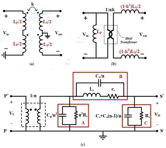
Figure 1.
Voltage transformer balun and its equivalent circuit. (a) Traditional transformer balun. (b) Equivalent model with a limited k value. (c) Equivalent circuit in high frequency (with k = 1).
The equivalent circuit of a single RF transformer at high frequency is shown in Figure 1c. Replacing n with allows for a discussion of the impact of k, where a larger k is known to improve the transformer’s transmission characteristics.
The leakage inductance and parasitic capacitance result in an equivalent parallel resonance for the non-inverting transformer, leading to amplitude and phase imbalances near the resonant frequency [15]. The of a transformer with inverting and non-inverting connections can be analyzed using the following equation:
where A, B, and C are impedances of the three corresponding circuit blocks in Figure 1c, and n is the ratio turns of windings.
Using Equation (3), the theoretical high-frequency performance curves of the inverting transformer and non-inverting transformer can be plotted as shown in Figure 2, which is consistent with published results of [15]. The simulation curve in Figure 2 illustrates the frequency-dependent insertion loss characteristics of an ideal transformer under both positive and negative coupling conditions, taking into account inter-winding parasitic capacitance at high frequencies. When the model shown in Figure 1c is configured using the parameters specified in the caption of Figure 2, the resulting high-frequency response of the equivalent model closely matches the simulation curve. This strong correlation confirms the effectiveness and accuracy of the proposed model in the high-frequency range.
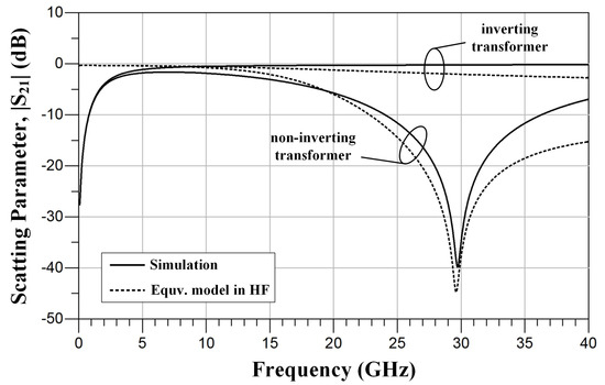
Figure 2.
Theoretical insertion loss curve (Ls = 862 pH, Cp = 52.7 fF, Cs = 91.5 fF, Co = 33.5 fF, rs = 2.03 Ω, Rs = 7.5 kΩ, k = 0.85, n = ±1).
2.2. Voltage Transformer Balun
The traditional transformer balun schematic, as depicted in Figure 1a, consists of a transformer with the primary inductor connected single-ended and the secondary inductor connected differentially. This configuration is equivalent to two transformers, with one being non-inverting connected and the other being inverting connected.
In transformer-based baluns, the phase difference at the balanced output ports typically originates from a pair of transformers (TFs) with opposite coupling polarities, forming the fundamental structure. As demonstrated in [16,17], the ABCD matrix of an ideal transformer with a turns ratio of N:1, consisting of a primary winding and a secondary winding , is given by
As established in [18], the turns ratio N relates to the coupling coefficient (k) through the following expression:
The sign of the coupling coefficient k typically indicates whether the coil windings exhibit positive or negative magnetic coupling. As shown in Equation (5), the sign of the turns ratio N corresponds to the sign of k. Substituting this relationship into Equation (4) reveals that the phase of the ideal transformer’s transmission coefficient is determined by k—specifically, whether the transformer utilizes positive or negative coupling. This sign difference in k ultimately results in the phase shift at the output ports. The theoretical analysis of the balun presented in this work is fundamentally based on this principle.
From the previous section, it is apparent that the bandwidth of a voltage transformer balun is limited by the non-inverting transformer at the high-frequency end. At the low-frequency end, a voltage transformer balun is primarily constrained by the limited on-chip inductance value, which can be improved by adding capacitors that are in parallel to the primary and secondary inductors in the transformer, which will impact performance at the high-frequency end [15].
2.3. Current Transformer Balun
Guanella baluns, also referred to as current baluns, can achieve wider bandwidth than voltage transformer baluns. In integrated circuits, Guanella baluns can be implemented using transformers, as depicted in Figure 3a. The equivalent circuit of a Guanella balun is illustrated in Figure 3b, where symbolizes the magnetizing inductance of the transformer, while , , and denote the characteristic impedances of Port 1, Port 2, and Port 3, respectively.
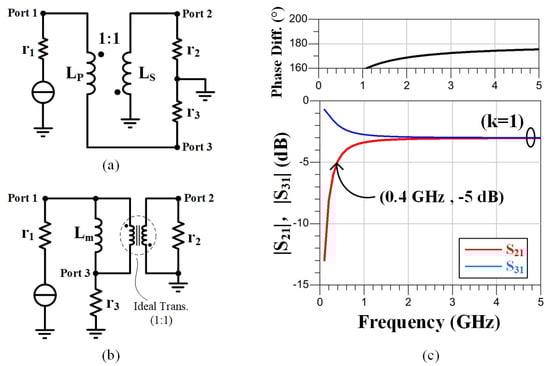
Figure 3.
(a) Schematic and (b) equivalent circuit of Guanella balun; (c) insertion loss and phase difference of the Guanella balun = = 10 nH.
The current balun achieves signal balance by altering the current phase, thereby ensuring equal but opposing currents flow through each branch of the balanced connection.
Upon analyzing the Guanella balun circuit, the insertion losses and can be expressed as
For a 1:1 balun, = . By substituting the equivalent circuit parameters in Figure 3b, the and approaches the desired values of −3 dB at the high frequency range and the phase difference approaches .
It is evident that the Guanella balun exhibits excellent amplitude and phase performance at the high frequency range between the positive and negative paths, contributing to its significantly broad bandwidth. However, at lower frequencies, the limited magnetizing inductance () causes current leakage from Port-1 through , resulting in higher amplitude at Port-3 compared to Port-2 and phase imbalance, as shown in Figure 3c.
2.4. Ultra-Wideband Balun
By analyzing the bandwidth limitations of voltage transformer and current baluns, an ultra-wideband balun is proposed in Figure 4a, leveraging the strengths of each. This balun capitalizes on the superior performance of the inverting transformer in the traditional voltage balun and that of the Guanella current balun at high frequency ranges. Additionally, to enhance performance at lower frequency ranges, an additional third inductor is incorporated in the topology.
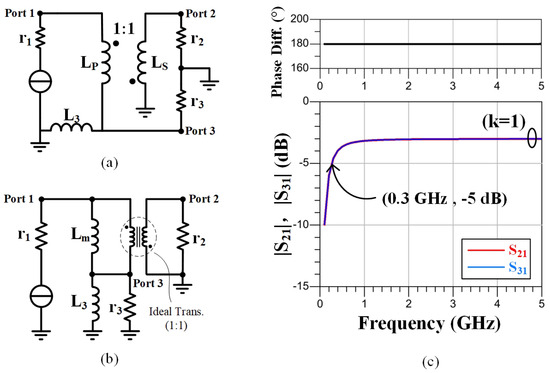
Figure 4.
(a) Schematic and (b) equivalent circuit of the ultra wideband balun; (c) insertion loss and phase difference of the ultra wideband balun = = = 10 nH.
In the previous section, we discussed how the bandwidth of a voltage transformer balun is restricted by its non-inverting transformer at high frequencies, primarily due to parasitic capacitance between the primary and secondary windings. Conversely, the inverting transformer exhibits broadband characteristics, attributed to an equivalent “negative capacitor” providing a “zero” for the system [15] or an equivalent “negative inductor” in the T-section model, thus expanding the high-frequency bandwidth.
Considering limited on-chip inductances and assuming perfect magnetic coupling between the primary and secondary inductors, the proposed ultra-wideband balun uses an inverting transformer with identical primary () and secondary () inductors to generate the negative signal. An additional third inductor () with the same inductance is introduced between and ground (), facilitating the positive signal generation from the node between and .
It is noteworthy that the proposed balun functions as a Guanella current balun at higher frequencies and as a voltage balun at lower frequencies. In the higher frequency range, when the impedance of the inductors is high and under perfect magnetic coupling conditions (k = 1), as illustrated in Figure 4b, the resistance is transferred to the primary side due to the inverter transformer connection. Given that and , a balanced condition emerges in the resulting bridge circuit. Consequently, no current flows from the top of to the top of (the third inductor), forcing equal-magnitude but opposite-direction currents () into the positive and negative branches. However, as the frequency decreases, more current begins to flow through the third inductor due to the limited magnetizing inductance value.
The equivalent circuit model of the ultra-wide balun is depicted in Figure 4b, by analyzing this circuit model, we can express the insertion losses and of the ultra-wideband balun circuit as follows:
The enhanced bandwidth performance is illustrated in Figure 4c, where the third inductor () has the same value as the magnetizing inductor (). Comparing of Figure 3c and Figure 4c, the proposed topology maintains the phase difference and amplitude balance between the two outputs all the way down to DC. While amplitude degradation at lower frequencies occurs at a slower rate compared to the current transformer balun, indicating an expanded operating bandwidth.
In practical design scenarios, where the coupling coefficient (k) is less than 1 and the influence of leakage inductance must be accounted for, the equivalent circuit model of the proposed balun topology can be illustrated as depicted in Figure 5. Assuming a 1:1 transformer with a 1: = 1 configuration, the insertion losses and can be derived:
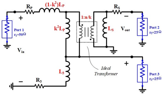
Figure 5.
Ultra-wideband balun with leakage and parasitic resistor.
Under ideal conditions with perfect magnetic coupling (k = 1) and lossless inductors ( = = = 0) in the circuit model, Equations (10) and (11) can be simplified to Equations (8) and (9).
A key feature enabling the wide bandwidth of the proposed balun topology is the generation of positive and negative signals using distinct schemes across different frequency ranges. This allows the balun to be optimized for a wider bandwidth compared to other topologies such as the voltage transformer balun or current balun. This flexibility is demonstrated by the optimization of the relative inductance among the three inductors and the mitigation of parasitic capacitance through layout design.
For a 1:1 inverting transformer generating the negative signal, and should ideally be equal. However, due to leakage inductance (as depicted in Figure 5), must be larger than to maintain a consistent voltage difference. To ensure balanced positive and negative outputs, (equal to ) should closely match . In practice, the coupling coefficient k is typically less than 0.8, so as is less than .
The preceding analysis assumes ; however, in practical implementations, frequency-dependent variations occur between and due to skin and proximity effects. Consequently, this assumption does not hold across the full frequency spectrum. More importantly, the ideal coupling condition (k = 1) is not achievable in integrated circuits. These non-idealities introduce significant discrepancies in both qualitative and quantitative circuit analyses, ultimately leading to amplitude and phase imbalances in the balun’s performance across varying operating frequencies.
Besides the inductance values, the parasitic capacitance associated with the inverting transformer and the third inductor can significantly impact the balun’s frequency capability at the high end. These parasitic capacitances can be separately changed through layout optimization. As an example, the negative signal response can be optimized by exploring the impact of parasitic capacitance in the transformer layout. As illustrated in Figure 6, the bridge/parasitic capacitance () between the windings can noticeably affect the inverting transformer’s insertion loss. Therefore, improved performance can be achieved by fine-tuning the layout to increase the parasitic capacitance between the windings or by incorporating additional capacitors into the design.
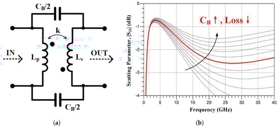
Figure 6.
(a) Schematic diagram and (b) curve of the impact of bridge capacitors on inverter transformers. ( = = 1.5 nH, = 100 fF, k = 0.9).
As shown in Figure 7b, floating metal strips are periodically arranged above or below the planar coupled inductor traces of the balun, with their orientation perpendicular to the inductor plane. This validated technique enables effective fine-tuning of amplitude and phase errors across different frequency bands. Crucially, these floating strips remain unconnected to any potential, thus avoiding excessive electromagnetic interference or introducing additional losses to the balun. Moreover, their flexible vertical positioning enables localized adjustments of the equivalent permittivity around the traces, allowing precise tuning of distributed to optimize performance.
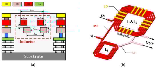
Figure 7.
(a) Simplified metal stackes structure. (b) Proposed layout of the ultra-wideband blaun.
Although the Ruthroff balun [19] and the config K balun [20] from Mini-circuits share similarities with the ultra-wideband balun discussed in this paper, they also exhibit notable differences. Built with wires wound around magnetic core material, the Ruthroff and Mini-circuits baluns operate as transmission line transformers which can operate at low frequency naturally, and the third inductor is used only to complete the DC path.
3. Balun Design, Simulation, and Measurement
An ultra-wideband planar balun was designed using a commercial 45 nm RFE process from GlobalFoundries. This process offers an RF-friendly BEOL with thick Cu metal and a high-resistivity substrate. The simplified laminate structure of 45 nm RFE process is illustrated in Figure 7a, where the metal layers M1 and M2 used for inductor design have a thickness of 3 m each.
The equivalent schematic of the balun with the most important component values is shown in Figure 8a. It can be seen that the three inductor values are different with a coupling coefficient of 0.788. The value of is much higher than and according to the inductance ratio: = , indicating an equivalent inverting transformer ratio of 1:1.
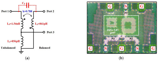
Figure 8.
(a) Schematic of ultra-wideband planar balun. (b) Picture of the ultra-wideband balun.
The balun layout is shown in Figure 8b, with the inverting transformer designed using edge coupling at the same metal layers. The third inductor is placed away from the inverting transformer. The overall dimensions are approximately 265 m × 141 m.
Electromagnetic simulations were conducted using the EMX simulator integrated into the Cadence Virtuoso environment. The simulation results, as shown in Figure 9, demonstrate that the proposed wideband balun achieves excellent amplitude and phase balance, as well as low insertion loss. The minimum insertion loss (IL) of the circuit is −0.73 dB, with a −1 dB bandwidth ranging from 10.9 to 41.1 GHz and a −2 dB bandwidth spanning from 4.9 to 42.8 GHz.
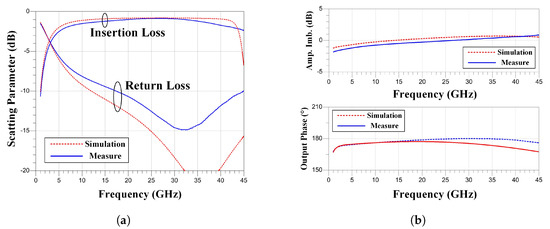
Figure 9.
Simulation and measurement. (a) Insertion loss and return loss. (b) Amplitude imbalance and phase imbalance.
The measurement result deviates from the simulation at the high-frequency end, which may be due to parasitic effects caused by the probe pads and the connecting transmission lines. (The measurement shows that the insertion loss is approximately −1.2 dB, and the bandwidth of −3 dB is 4.1∼45+ GHz. The amplitude imbalance is 0.16 ± 0.85 dB, and the phase imbalance is 1 ± ).
Compared to other on-chip broadband baluns, the proposed design offers reduced size and increased relative bandwidth with good IL performance, as shown in Table 1.

Table 1.
Comparison of this balun and others.
4. Mixer with an Ultra-Wideband Balun
The operating bandwidth of a double-balanced passive mixer is dominated by the bandwidth of the baluns. To demonstrate the wide bandwidth of the proposed ultra-wideband balun, a double-balanced mixer with broad frequency coverage has been developed and fabricated [26].
The mixer’s RF, IF, and LO ports are all 50 (single-ended) with integrated baluns for the RF and IF ports. The integrated RF balun is optimized to cover a frequency range of 2∼14 GHz, while the integrated IF balun is optimized to cover a frequency range of 0.5∼6 GHz [27]. The parasitic capacitance introduced by the mixer at the balun output port facilitates impedance matching, as evidenced by [28].
The mixer, packaged in a tiny 2 × 3 mm QFN, is biased by a 3.3 V supply, and the current consumption is 132 mA at room temperature. The measured conversion loss and return loss performance are illustrated in Figure 10. When compared to other broadband mixers available on the market, the mixer designed with the ultra-wideband balun stands out by offering the broadest RF and IF bandwidths. Additionally, this mixer maintains excellent impedance matching across the entire frequency range while delivering superior linearity performance at low LO input power.
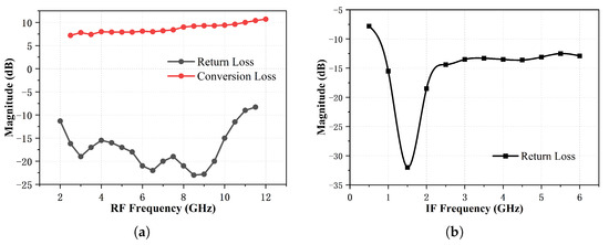
Figure 10.
Measured performance of the broadband double-balanced mixer. (a) Conversion loss and return loss at the RF port vs. RF frequency (Low Side LO). (b) Return loss at the IF port vs. IF Frequency (Low Side LO).
5. Conclusions
In conclusion, this paper presents an analysis of the bandwidth limitations of voltage transformer baluns and current baluns. An ultra-wideband balun topology is investigated, designed and fabricated using a commercial 45 nm RFE process. The measurement results demonstrate that, in comparison to other integrated balun topologies, the proposed ultra-wideband balun exhibits a broader operational bandwidth, as well as superior amplitude and phase balance. The design was further validated by integrating the balun topology into a broadband double-balanced mixer, which showcased exceptional performance across a wide frequency range. These results highlight the potential of the proposed broadband balun as a promising solution in the design of broadband mixers and other RF circuits that necessitate wide operating bandwidth and precise amplitude and phase balance.
Author Contributions
Conceptualization, X.W.; methodology, X.W.; software, X.Z.; validation, X.W. and X.Z.; formal analysis, X.Z.; investigation, X.W. and X.Z.; resources, X.W.; data curation, X.Z.; writing—original draft preparation, X.Z.; writing—review and editing, X.Z., H.X., B.B. and X.W.; visualization, X.Z.; supervision, X.W.; project administration, X.W.; funding acquisition, X.W. All authors have read and agreed to the published version of the manuscript.
Funding
This research was funded by the Fundamental Research Funds for the Central Universities, Nankai University (63241330).
Data Availability Statement
Data is contained within the article.
Acknowledgments
The authors would like to thank GlobalFoundries for providing silicon fabrication through the 45RFE university program.
Conflicts of Interest
The author Bill Beckwith was employed by the company The Analog Devices Inc. The remaining authors (X.Z., H.X., and X.W.) declare that the research was conducted in the absence of any commercial or financial relationships that could be construed as a potential conflict of interest.
References
- Ma, S.; Wu, T.; Zhang, J.; Ren, J. A 5G Wireless Event-Driven Sensor Chip for Online Power-Line Disturbances Detecting Network in 0.25 μm GaAs Process. IEEE Trans. Ind. Electron. 2021, 68, 5271–5280. [Google Scholar] [CrossRef]
- Chakraborty, S.; Milner, L.E.; Zhu, X.; Hall, L.T.; Sevimli, O.; Heimlich, M.C. A K-Band Frequency Doubler with 35-dB Fundamental Rejection Based on Novel Transformer Balun in 0.13-μm SiGe Technology. IEEE Electron Device Lett. 2016, 37, 1375–1378. [Google Scholar] [CrossRef]
- Chakraborty, S.; Milner, L.E.; Zhu, X.; Sevimli, O.; Parker, A.E.; Heimlich, M.C. An Edge-Coupled Marchand Balun With Partial Ground for Excellent Balance in 0.13 μm SiGe Technology. IEEE Trans. Circuits Syst. II Express Briefs 2021, 68, 226–230. [Google Scholar] [CrossRef]
- Huang, C.H.; Chen, C.H.; Horng, T.S. Design of integrated planar Marchand balun using physical transformer model. In Proceedings of the 2009 Asia Pacific Microwave Conference, Singapore, 7–10 December 2009; pp. 1004–1007. [Google Scholar] [CrossRef]
- Tseng, S.C.; Meng, C.; Chang, C.H.; Wu, C.K.; Huang, G.W. Monolithic Broadband Gilbert Micromixer With an Integrated Marchand Balun Using Standard Silicon IC Process. IEEE Trans. Microw. Theory Tech. 2006, 54, 4362–4371. [Google Scholar] [CrossRef]
- Marchand, N. Transmission line conversion transformers. Electronics 1944, 17, 142–145. [Google Scholar]
- Deb, P.K.; Moyra, T.; Bhhattacharyya, B.K. Miniaturized and enhanced bandwidth Marchand Balun using CSRR. IET Microw. Antennas Propag. 2021, 15, 788–796. [Google Scholar] [CrossRef]
- Costantini, A.; Lawrence, B.; Mahon, S.; Harvey, J.; McCulloch, G.; Bessemoulin, A. Broadband Active and Passive Balun Circuits: Functional Blocks for Modern Millimeter-Wave Radio Architectures. In Proceedings of the 2006 European Microwave Integrated Circuits Conference, Manchester, UK, 10–13 October 2006; pp. 421–424. [Google Scholar] [CrossRef]
- Chen, T.; Chang, K.; Wang, H.; Dow, G.; Liu, L.; Bui, S.; Lin, T. Broadband monolithic passive baluns and monolithic double-balanced mixer. In Proceedings of the 1991 IEEE MTT-S International Microwave Symposium Digest, Boston, MA, USA, 10–14 July 1991; Volume 2, pp. 861–864. [Google Scholar] [CrossRef]
- Dai, Y.S.; Li, X.; Zhu, D. Ultra compact wideband Balun design and realization based on LTC. J. Microw. 2014, 30, 4. [Google Scholar]
- Wu, B.; Ji, Y.; Fang, G. An improved ultra wide-bandwidth planar Balun. J. Univ. Chin. Acad. Sci. 2010, 27, 507–511. [Google Scholar]
- Lin, Z.; Zhang, S.; Jia, D.; Liang, X.; Deng, J.; Nian, F. Design of a 35-95 GHz fundamental monolithic mixer based on a novel IF extraction structure. IEICE Electron. Express 2019, 16, 20190602. [Google Scholar] [CrossRef]
- Wang, X. Novel Broadband Balun Structures and Their Applications. Chinese Patent CN116799463A; granted, 15 September 2023. [Google Scholar]
- Zhu, X.; Xu, H.; Xia, T.; Wang, X. Invited Paper: Comparison and Analysis of on-Chip Broadband Integrated Balun. In Proceedings of the 2024 IEEE 67th International Midwest Symposium on Circuits and Systems (MWSCAS), Springfield, MA, USA, 11–14 August 2024; pp. 152–156. [Google Scholar] [CrossRef]
- Long, J. Monolithic transformers for silicon RF IC design. IEEE J. Solid-State Circuits 2000, 35, 1368–1382. [Google Scholar] [CrossRef]
- Jurgen, R.K. Ideal Transformers and Coupled Inductors. In Linear Circuits; Addison-Wesley: Reading, MA, USA, 1982; Chapter 5. [Google Scholar]
- Pozar, D.M. Microwave Engineering, 4th ed.; Original English edition; John Wiley & Sons: Hoboken, NJ, USA, 2011; p. 752. [Google Scholar]
- Que, X.; Jiang, L.; Wang, Y. A Novel Compact Uniplanar Isolation Circuit for Three-Port Baluns. In Proceedings of the 2024 IEEE/MTT-S International Microwave Symposium—IMS 2024, Washington, DC, USA, 16–21 June 2024; pp. 289–292. [Google Scholar] [CrossRef]
- Sevick, J.; W2FMI. More On The 1:1 Balun. CQ Amateur Radio 1994, 50, 26–46. [Google Scholar]
- Yu, W.; Sengal, U. Demystifying RF Transformers. Microw. J. 2020, 62, 52. [Google Scholar]
- Yang, Y.; Wu, Y.; Zhuang, Z.; Kong, M.; Wang, W.; Wang, C. An Ultraminiaturized Bandpass Filtering Marchand Balun Chip With Spiral Coupled Lines Based on GaAs Integrated Passive Device Technology. IEEE Trans. Plasma Sci. 2020, 48, 3067–3075. [Google Scholar] [CrossRef]
- Yang, G.; Wang, K.; Wang, Z. 20.8-51 GHz highly balanced CMOS Balun. Electron. Lett. 2017, 53, 1202–1203. [Google Scholar] [CrossRef]
- Chakraborty, S.; Milner, L.E.; Zhu, X.; Parker, A.; Heimlich, M. Analysis and Comparison of Marchand and Transformer Baluns Applied in GaAs. IEEE Trans. Circuits Syst. II Express Briefs 2022, 69, 4278–4282. [Google Scholar] [CrossRef]
- Chang, C.F.; Lin, Y.S. On-chip transformer-coupled balun bandpass filter for 5-GHz applications. In Proceedings of the 2015 IEEE MTT-S International Microwave Symposium, Phoenix, AZ, USA, 17–22 May 2015; pp. 1–4. [Google Scholar] [CrossRef]
- Li, Y.; Zhu, X.W.; Tian, L.; Liu, R.J. Compact 2-18 GHz on-chip Balun based on centrosymmetric spiral transformers. Electron. Lett. 2020, 56, 229–230. [Google Scholar] [CrossRef]
- Wang, X.; Beckwith, W.; Schiltz, T. Broadband Integrated RF/Microwave/Millimeter Mixer with Integrated Balun(s). U.S. Patent US9,312,815; granted, 12 April 2016. [Google Scholar]
- Analog Devices, Inc. LTC5549 Data Sheet; Analog Devices, Inc.: Wilmington, MA, USA, 2020; Available online: https://www.analog.com/media/en/technical-documentation/data-sheets/5549fa.pdf (accessed on 1 June 2024).
- Chakraborty, S.; Milner, L.E.; Parker, A.; Heimlich, M. A Folded Edge-Coupled Transformer Balun in GaAs with Excellent Balance from 9 to 20 GHz. In Proceedings of the 2018 48th European Microwave Conference (EuMC), Madrid, Spain, 23–27 September 2018; pp. 1101–1104. [Google Scholar] [CrossRef]
Disclaimer/Publisher’s Note: The statements, opinions and data contained in all publications are solely those of the individual author(s) and contributor(s) and not of MDPI and/or the editor(s). MDPI and/or the editor(s) disclaim responsibility for any injury to people or property resulting from any ideas, methods, instructions or products referred to in the content. |
© 2025 by the authors. Licensee MDPI, Basel, Switzerland. This article is an open access article distributed under the terms and conditions of the Creative Commons Attribution (CC BY) license (https://creativecommons.org/licenses/by/4.0/).