However, due to the internal heat, ambient temperature, aging effects, and industrial errors, there is usually a ±10% parametric deviation from the nominal value for each component. The parametric deviation can make it difficult for the DS-LCC compensation topology to maintain resonance and, furthermore, cause the loss of the load-independent constant current output characteristics. Therefore, it is of great interest to reduce the effect of the parametric deviation on the load-independent constant current output characteristics of the DS-LCC compensation topology.
2.1. Effect of the Parametric Deviation on the Load-Independent Constant Current Output Characteristics
An analysis of (6), (7), and
Figure 2 indicates that for the DS-LCC compensation topology, the first-stage L-circuit and the second-stage π-circuit are required to be in resonance at the same time for implementing the load-independent constant current output. However, the parametric deviation of the compensation elements may lead to different resonant frequencies for the L-circuit and π-circuit. This implies that it is difficult to compensate for the parametric deviation through the frequency-tracking technique alone. Therefore, the optimal design method of the compensating element needs to be further investigated in order to reduce the effect of the parametric deviation on the load-independent constant output characteristics for the L-circuit and π-circuit.
In accordance with
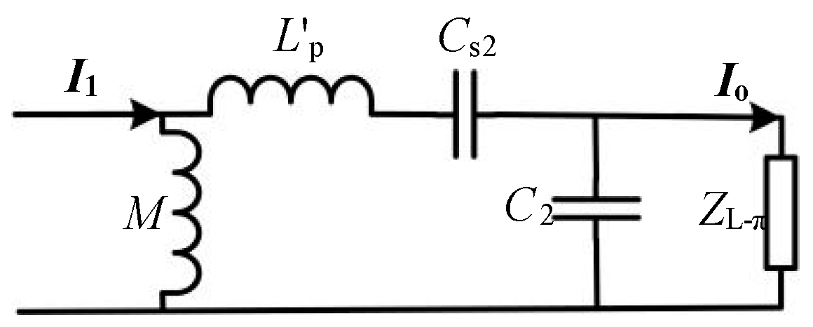
Figure 2, the π-circuit consisting of
L′p,
M,
Cs2, and
C2 can further be represented, as in
Figure 3, where the equivalent load
ZL-π, consisting of the compensation inductor
L2 and load
R′L, can be expressed as (8).
On the basis of
Figure 3 and (1), the current gain
gπ can be deduced as
As can be gathered from (9), if the operating frequency
ω, and the compensation elements
Lp,
Cs2, and
C2 are designed to satisfy the condition in (6), the load-independent constant output characteristics of the π-circuit can be realized. This indicates that if there is the parametric deviation in the element
Lp,
Cs2, or
C2, the resonant frequency
ω0 is bound to fluctuate, which causes the π-circuit to be detuned. Consequently, there must be a deviation factor
λp1, presented as (10), between the operating frequency
ω and the resonant frequency
ω0.
where
Lp0,
Cs20, and
C20 are the ideal value of corresponding components.
From (10), when there is the ±10% parametric deviation in compensation elements
Lp,
Cs2, and
C2, the fluctuation range of the deviation factor
λp1 is ±10%. This suggests that the parametric deviation of components
Lp,
Cs2, and
C2 can be equated to the fluctuation of the deviation factor
λp1. Hence, to analyze the effect of deviation factor
λp1 fluctuations on the load-independent output characteristics of the π-circuit,
Figure 3 can be further equated to
Figure 4, where the series connection of
L′p and
Cs2 is equated to the series connection of equivalent inductance
Leq and capacitance
Ceq, and their relation can be represented as
Substituting (11) into (9), the current gain can further be derived as
Based on (12), there always exists a set of
Leq and
Ceq, regardless of the parametric deviation of the components, in which the capacitance
Ceq enables the condition in (13) to be satisfied. This demonstrates that in this equivalent model, the circuit consisting of
M and
Ceq remains resonant at all times.
From (10), (12), and (13), the current gain can be simplified as
where
From (15), the variation in the load R′L can be equated to the fluctuation of Qπ. According to (14), when λp1 ≠ 1, the current gain must vary with fluctuations in Qπ, i.e., the load-independent constant current characteristic is lost. Therefore, it is necessary to investigate how to design the capacitance ratio n to enable the π-circuit to equivalently maintain the load-independent constant current characteristics.
Based on (14), it is difficult to directly analyze the design method of the capacitance ratio. Therefore, the deviation rate
ηπ of the current gain is defined as
Based on (16), the deviation rate
ηπ of the current gain as the function of capacitance ratios
n can be expressed in
Figure 5 under different tolerance factors
λp1 and
Qπ. It can be observed from
Figure 5 that when
λp1 ≠ 1, the deviation
ηπ gradually increases with the increase in capacitance ratio
n. In addition, in comparison with
Figure 5a–d, under the same capacitance ratio
n, the larger
Qπ is, the smaller the deviation
ηπ is. As a result, for the π-circuit, reducing the capacitance ratio
n and increasing
Qπ by the parameter optimization can effectively minimize the deviation rate
ηπ of the current gain when
λp1 ≠ 1.
Further, it can be noted from (8) and (15) that the variation in the load
R′L can be equated to the fluctuation of
Qπ. The comparison of
Figure 5c,d indicates that when
Qπ = 0.8 and
Qπ = 1.6, the deviation
ηπ of the output current remains basically the same at the capacitance ratio
n < 0.5, i.e., the load-independent output characteristics can still be implemented. However, from
Figure 5a,b, when
Qπ = 0.2 and
Qπ = 0.4, the deviation
ηπ of the output current fluctuates significantly at
n < 0.5. This suggests that a larger
Qπ in the load range is better. From (6) and (15), an increase in
Qπ can be achieved by decreasing the capacitance ratio
n without changing the resonant frequency and equivalent load of the system. Therefore, for the π-circuit, lowering the capacitance ratio
n not only reduces the effect of the parametric deviation on the load-independent constant current, but also reduces the fluctuation of the output current.
Furthermore, the analysis of (15) reveals that the parametric deviation of the compensation capacitors
C2 and
Cs2 lead to fluctuations in the capacitance ratio. Thus, the fluctuation range
D of the capacitance ratio can be further represented as
where
a1 and
b1 are the ratios of the actual to ideal values for the compensation capacitors
C2 and
Cs2.
From (18), when parameter deviations of compensation capacitors are
Cs2 and
C2, i.e.,
a1,
b1 ∈ [0.9, 1.1], the fluctuation range is
D ∈ (0.82, 1.22). From
Figure 5, when
λp1 ≠ 1, the smaller the capacitance ratio
n, the smaller the output current deviation
ηπ under
D ∈ (0.82, 1.22). Consequently, at the low capacitance ratio, capacitance ratio fluctuations caused by the parametric deviation of compensation capacitors
Cs2 and
C2 have little effect on the load-independent output characteristics.
Then, in order to analyze the load-independent constant output characteristics of the L-circuit under the parametric deviation,
Figure 2 can be further equated to
Figure 6, where equivalent impedance
Zp of the secondary side can be expressed as (19).
From
Figure 6, the output current
I1 and output voltage
Uc1 of the L-circuit can be expressed as (20) and (21).
where
From (20), if compensating elements L1 and C1 are designed to satisfy the condition in (6), the current I1 remains constant and is unaffected by variations in the equivalent load ZL-L of the L-circuit. Similarly, the ±10% parametric deviation in the compensating elements L1 and C1 inevitably leads to λ1 ≠ 1, and the loss of the load-independent constant output characteristics.
To still maintain the load-independent constant output characteristics of the L-circuit, from (21), the output voltage deviation rate
ηL = |
Uc1(
λ1≠1)|/|
Uc1(
λ1 = 1)| as the function of
QL can be shown in
Figure 7 under different
λ1. As illustrated in
Figure 7, the deviation rate
ηL remains essentially constant over the larger range of
QL. Consequently,
QL should be designed to be as large as possible during the load
RL range.
In order to investigate the method for increasing
QL, through the parameter optimization, based on (6), (19), and (22), it can be further denoted as
From (23), the reduction in the capacitance ratio n can not only lead to an increase in QL at the same load R′L but also reduce the fluctuation in QL caused by load variations. This means that QL remains almost constant over the load range. As a result, the load-independent constant output of L-circuit can be equivalently implemented by reducing the capacitance ratio.
Based on the above analysis, it can be concluded that reducing the capacitance ratio can enable the DS-LCC compensation network to maintain the load-independent constant output characteristics under the parametric deviation of the compensation element. However, from [
23], when the rectifier is not operated in continuous mode, the system could still lose the load-independent constant output. Therefore, the boundary condition between the continuous and discontinuous mode needs to be derived and always keep the rectifier in the continuous mode under the parametric deviation.
The load current
IR depends on the average value of the current
i0 and can be expressed as (24).
According to
Figure 1, furthermore, the load voltage
UR can be derived as
where
For the rectifier, the voltage
UC2 should be greater than the load voltage
UR for operation in the continuous mode. Therefore, based on (24) and (25), the boundary condition for the continuous mode can be deduced as
It can be observed from (27) that the compensation inductance L2 should be slightly larger than the ideal value to ensure that the rectifier operates in the continuous mode.
From (4) and (7), the parametric deviation not only affects the load-independent constant output characteristics, but also cause fluctuations in the transmission gain
g. Based on (14) and
Figure 5, under the parametric deviation, the current gain of the π-circuit can be maintained as a constant also through reducing the capacitance ratio. However, according to (20), for the L-circuit, the current
I1 fluctuations caused by the parametric deviation are unavoidable. Hence, the conventional FM control can be adopted to achieve the constant current
I1, and the current
I1 can be further deduced as
where
a1 and
b1 are the deviation coefficients of
L1 and
C1, and can be denoted as
It can be observed from (28) that under the parametric deviation of L1 and C1, the constant output current I1 can be achieved by the FM control.
2.2. Implementation of the Soft Switching
For an IPT system, it is essential to implement the soft switching over the load range to improve efficiency. Since the IPT system generally operates at a higher frequency, the inverter is generally composed of MOSFETs. Hence, ZVS is more conducive to minimizing losses than the zero current switching. For the MOSFET, if the turn-off current
Ioff satisfies the condition in (30), ZVS can be implemented [
24].
where
Cj and
td denote the junction capacitance and dead time.
For an IPT system, the imaginary part of the input impedance is required to be greater than zero for implementing ZVS. Therefore, on the basis of (2) and (6), the input impedance of the system can be deduced as
where
It can be observed from (31) that the parametric deviation of the compensation elements L2, C2, C1, and Cs1 may cause the imaginary part of the input impedance to be less than zero. However, from (6) and (15), with the constant resonant frequency, the compensation capacitance C2 decreases with the reduction in the capacitance ratio. Based on (32), the smaller the compensation capacitor C2 is, the smaller the impedance fluctuation caused by the parametric deviation of compensation elements L2 and C2.
Moreover, based on the above analysis of the L-circuit, FM control is employed to achieve the constant current I1. From (28), the impedance fluctuation of compensation capacitor C1 is small with the FM. Therefore, the parametric deviation of Cs1 should be the primary consideration to ensure the realization of ZVS.
In order to investigate the design constraints of the compensation capacitor
Cs1, the input current should be further investigated. From (31), the fundamental harmonic
Iin-1st of the input current can be expressed as
In addition,
L1 and
C1 compose an LC filter on the primary side, which causes the input current to contain high harmonic currents. The (2m + 1)th harmonics
Iin-(2m+1)th of the input current can be expressed as
Further, the input current for all higher harmonics can be derived as (35).
Based on (30) and (35), under the ±10% parametric deviation, for the realization of ZVS, the compensation capacitor
Cs1 should satisfy the condition in (36).


