Abstract
For the double-sided inductor–capacitor–capacitor (DS-LCC) compensation topology, the parametric deviation of compensation elements results in the mismatch between the resonant frequency and operating frequency. Furthermore, this mismatch leads to the loss of the load-independent constant output characteristics. Therefore, an innovative design approach based on the reduction in the capacitance ratio is proposed to attain the load-independent constant current under the parametric deviation. With the presented method, simply by reducing the compensation capacitor ratio, the load-independent constant current output characteristics can be preserved, and fluctuations in the transmission gain caused by the parametric deviation are minimized. This implies that when the constant transmission gain is achieved by the frequency modulation (FM) control, the required FM range can be reduced. Finally, from the experimental results, in the load range of 3 Ω to 33 Ω, compared to the high capacitance ratio, the load-independent constant current characteristics can be maintained at the low capacitance ratio. In addition, without parametric deviation, the transmission efficiencies at different capacitance ratios are basically the same at 93.5% and 94.2%, respectively. However, the transmission efficiencies under different parametric deviations at the low capacitance ratio are 87.4% and 84.9%, but only 73.9% and 68.2% at the high capacitance ratio.
1. Introduction
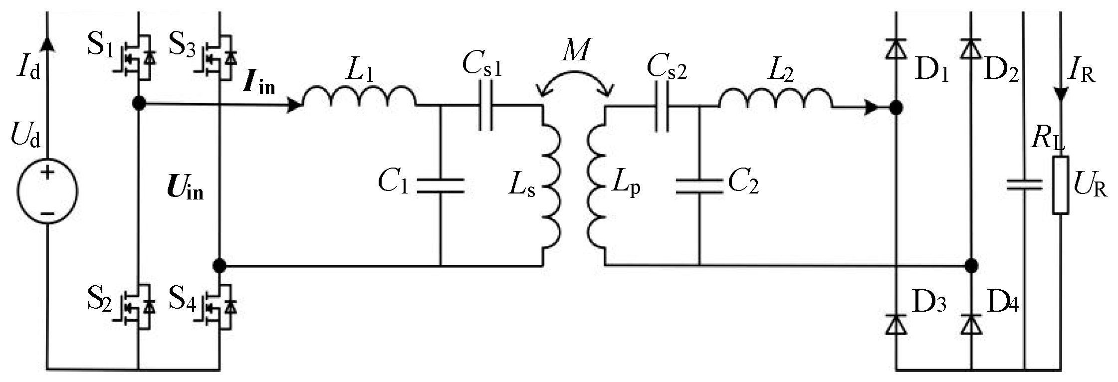
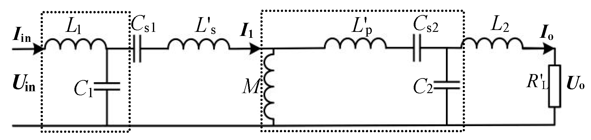
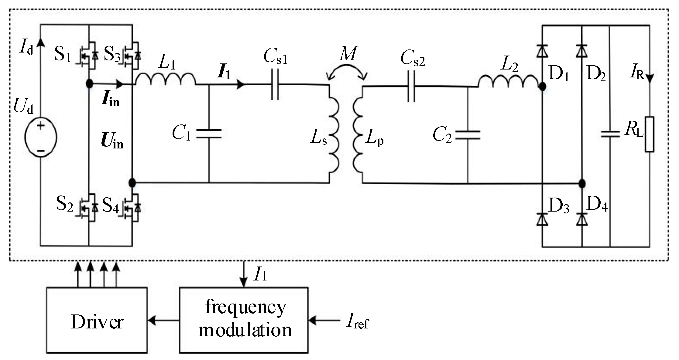
Inductive power transfer (IPT) technology is capable of transmitting energy through the high-frequency magnetic field without physical contact. This indicates that IPT technology, adopted in a variety of applications, such as implantable medical devices and electric vehicles, is promising, due to its advantages of weather proofing, higher convenience, and low maintenance [1,2,3]. The IPT system generally requires separate compensation circuits at the transmitter and receiver, respectively, to compensate for the leakage inductance and achieve the high-performance operation of the system. Figure 1 shows the DS-LCC compensation topology, in which there is an LCC circuit on both the transmitter and receiver. L1, C1, and Cs1 make up compensation elements of the transmitter. L2, C2, and Cs2 make up compensation elements of the receiver. Ls and Lp are the self-inductances of the transmitting coil and receiving coil. M depicts the mutual inductance. Switching devices S1–S4 compose the inverter at the transmitting side, while diodes D1–D4 compose the rectifier at the receiving side. Compared to lower order compensation networks such as SS compensation topology, this compensation topology offers greater design flexibility, multiple resonant points, a stable resonant frequency independent of the mutual inductance, and enhanced tolerance to the misalignment [4,5,6]. Its ability to maintain the load-independent constant output at the resonant frequency simplifies the control system design, making it a preferred choice in recent research [7,8]. However, due to a number of factors, such as the variation in the internal heat and ambient temperature, aging effect, and industrial error, the parameter of elements can deviate from their ideal values with the ±10% fluctuation [9]. The parametric deviation can cause the system to be detuned and further leads to the loss of the load-independent constant output characteristic. Therefore, for the DS-LCC compensation topology, it is of great significance that under the parametric deviation, the load-independent constant output characteristics can be implemented.
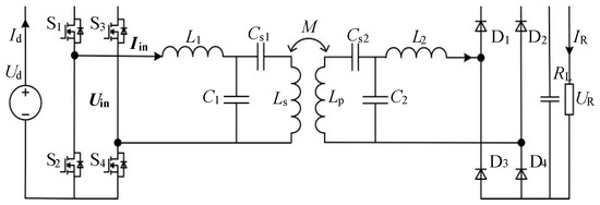
Figure 1.
Double-sided LCC compensation network.
Several methodologies are proposed to analyze parametric sensitivity and reduce the influence of the parametric deviation in compensation components. On the one hand, it is very effective to compensate for the output fluctuation resulting from the parametric deviation through different control strategies [10,11,12,13,14]. The constant output current of the S-LCC compensation topology can be achieved by employing the frequency tracking [10]. However, for the DS-LCC compensation topology, frequency tracking techniques may lead to the loss of the load-independent constant current characteristics and increase the complexity of the control system. Based on the SS compensation topology, a fractional-order IPT system is proposed to achieve the constant output [11]. Nevertheless, since there are many components, it is hardly possible to establish a fractional-order equivalent model of the DS-LCC compensation topology. Alternatively, the variable inductor and switched controllable capacitor (SCC) can also be adopted to compensate for the parametric deviation [12,13,14]. However, due to the larger number of components in the DS-LCC compensation topology, these methods will increase the complexity of the control system and also lead to a reduction in efficiency.
On the other hand, the optimal design of the compensation network seems to be another effective strategy [15,16,17,18,19,20]. The parametric sensitivity of the DS-LCC compensation topology is analyzed and it is noted that the parametric deviation of the primary series compensation capacitor and secondary compensation inductor have the least effect on the load-independent constant output characteristics [15,16]. Nevertheless, solutions for the parametric deviation of other components are not presented. Based on the parametric sensitivity analysis of the S-S-P network, the selection of higher precision compensation capacitors is proposed [17]. This method will undoubtedly increase the cost of the system. The optimally resonant mode can be selected by the comparison of the frequency sensitivity in different constant current modes of the DS-LCC compensation topology [18]. However, the correlation between the parametric deviation and resonant frequency variations has yet to be fully established. A combination of exhaustive and Monte Carlo stochastic analysis can be utilized to design the DS-LCC compensation circuit and the fluctuation of the output power is less than 10% over the ±10% range of the parametric deviation [19]. For implementing the constant voltage output of the LCC-S network under the parametric deviation in compensation capacitors, Sobol sensitivity analysis is employed to obtain the optimal parameter [20]. However, in both parameter optimization methods, the load-independent constant output characteristics cannot be attained.
Therefore, a distinctive design method is proposed to implement the load-independent constant current output characteristics under ±10% parametric deviations. In the proposed methodology, only through the reduction in the capacitance ratio, the load-independent constant current output characteristics can be maintained and transmission gain fluctuations caused by the parametric deviation are also reduced. This suggests that the constant transmission gain can be achieved through FM control alone, and the frequency adjustment range can be effectively reduced. In addition, for the IPT system, the imaginary part of the input impedance is generally required to be greater than 0 to realize zero voltage switching (ZVS) for efficiency enhancement. However, parametric deviation may also lead to fluctuations in the input impedance of the system, resulting in the loss of ZVS. Therefore, the ZVS realization condition of the proposed method is further investigated.
The following sections make up the rest of this paper: Section 2 analyzes the output characteristics of the equivalent π-circuit and the L-circuit under the parametric deviation in the load range is analyzed. Furthermore, the method based on the reduction in the capacitance ratio is proposed to reduce the output deviation caused by the parametric deviation. The ZVS condition is also deduced. The design procedure and construction of the proposed IPT system are presented in Section 3. In Section 4, simulation and experimental results are revealed and analyzed to validate the accuracy of the proposed method. Lastly, the paper is conclusively summarized in Section 5.
2. Realization of Load-Independent Constant Output Characteristics Under Component Parameter Deviations
The leakage equivalent circuit of the DS-LCC compensation topology is illustrated in Figure 2. Where the leakage inductance of the corresponding coil and equivalent load are represented as L′s, L′p, and R′L, and can be expressed as (1).
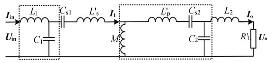
Figure 2.
Equivalent model of DS-LCC compensation topology.
From the leakage inductance model, the KVL equation can be derived as
where
It can be easily deduced from (2) that the transmission gain g, i.e., the ratio of the output current Io to the input voltage Uin, can be expressed as
where
In the conventional design method of the DS-LCC compensation topology [21,22], it can be deduced from (4) that the resonant frequency ω0 is generally designed to satisfy the condition in (6). Further, substituting (6) into (4), the output current Io is further deduced as (7), and from (7) the load-independent constant current output characteristics can be achieved.
However, due to the internal heat, ambient temperature, aging effects, and industrial errors, there is usually a ±10% parametric deviation from the nominal value for each component. The parametric deviation can make it difficult for the DS-LCC compensation topology to maintain resonance and, furthermore, cause the loss of the load-independent constant current output characteristics. Therefore, it is of great interest to reduce the effect of the parametric deviation on the load-independent constant current output characteristics of the DS-LCC compensation topology.
2.1. Effect of the Parametric Deviation on the Load-Independent Constant Current Output Characteristics
An analysis of (6), (7), and Figure 2 indicates that for the DS-LCC compensation topology, the first-stage L-circuit and the second-stage π-circuit are required to be in resonance at the same time for implementing the load-independent constant current output. However, the parametric deviation of the compensation elements may lead to different resonant frequencies for the L-circuit and π-circuit. This implies that it is difficult to compensate for the parametric deviation through the frequency-tracking technique alone. Therefore, the optimal design method of the compensating element needs to be further investigated in order to reduce the effect of the parametric deviation on the load-independent constant output characteristics for the L-circuit and π-circuit.
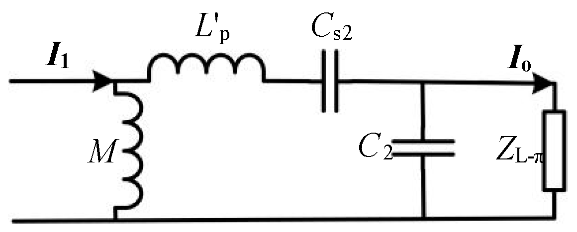
In accordance with Figure 2, the π-circuit consisting of L′p, M, Cs2, and C2 can further be represented, as in Figure 3, where the equivalent load ZL-π, consisting of the compensation inductor L2 and load R′L, can be expressed as (8).

Figure 3.
The π-circuit consisting of L′p, M, Cs2, and C2.
As can be gathered from (9), if the operating frequency ω, and the compensation elements Lp, Cs2, and C2 are designed to satisfy the condition in (6), the load-independent constant output characteristics of the π-circuit can be realized. This indicates that if there is the parametric deviation in the element Lp, Cs2, or C2, the resonant frequency ω0 is bound to fluctuate, which causes the π-circuit to be detuned. Consequently, there must be a deviation factor λp1, presented as (10), between the operating frequency ω and the resonant frequency ω0.
where Lp0, Cs20, and C20 are the ideal value of corresponding components.
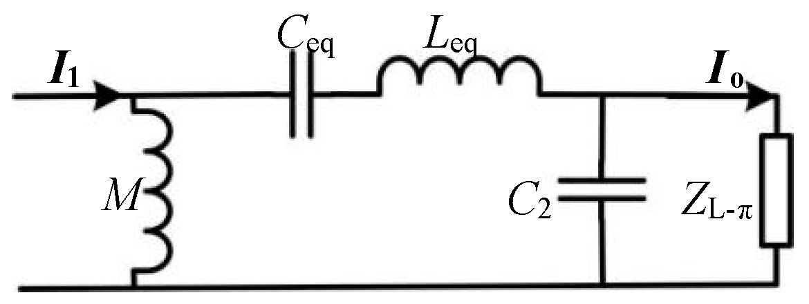
From (10), when there is the ±10% parametric deviation in compensation elements Lp, Cs2, and C2, the fluctuation range of the deviation factor λp1 is ±10%. This suggests that the parametric deviation of components Lp, Cs2, and C2 can be equated to the fluctuation of the deviation factor λp1. Hence, to analyze the effect of deviation factor λp1 fluctuations on the load-independent output characteristics of the π-circuit, Figure 3 can be further equated to Figure 4, where the series connection of L′p and Cs2 is equated to the series connection of equivalent inductance Leq and capacitance Ceq, and their relation can be represented as
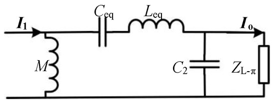
Figure 4.
The equivalent model of the π-circuit.
Substituting (11) into (9), the current gain can further be derived as
Based on (12), there always exists a set of Leq and Ceq, regardless of the parametric deviation of the components, in which the capacitance Ceq enables the condition in (13) to be satisfied. This demonstrates that in this equivalent model, the circuit consisting of M and Ceq remains resonant at all times.
From (10), (12), and (13), the current gain can be simplified as
where
From (15), the variation in the load R′L can be equated to the fluctuation of Qπ. According to (14), when λp1 ≠ 1, the current gain must vary with fluctuations in Qπ, i.e., the load-independent constant current characteristic is lost. Therefore, it is necessary to investigate how to design the capacitance ratio n to enable the π-circuit to equivalently maintain the load-independent constant current characteristics.
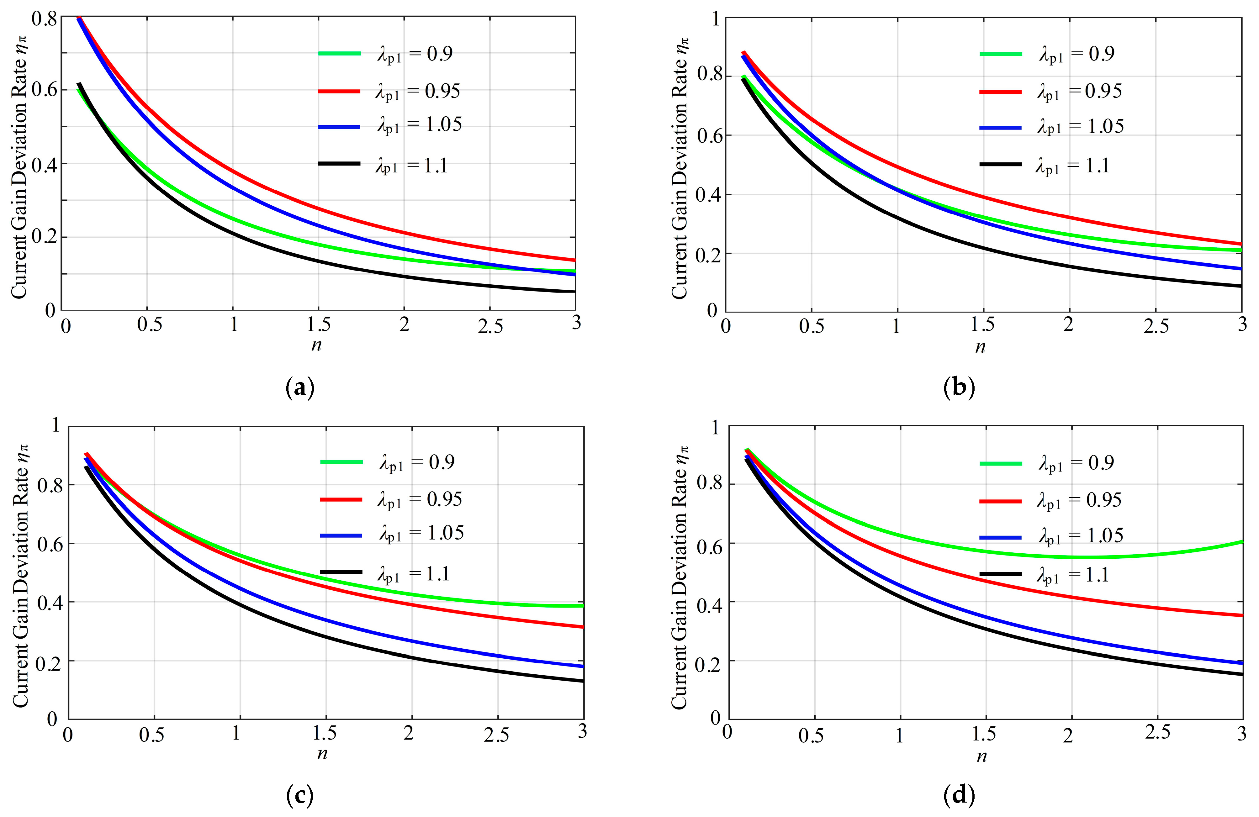
Based on (14), it is difficult to directly analyze the design method of the capacitance ratio. Therefore, the deviation rate ηπ of the current gain is defined as
Based on (16), the deviation rate ηπ of the current gain as the function of capacitance ratios n can be expressed in Figure 5 under different tolerance factors λp1 and Qπ. It can be observed from Figure 5 that when λp1 ≠ 1, the deviation ηπ gradually increases with the increase in capacitance ratio n. In addition, in comparison with Figure 5a–d, under the same capacitance ratio n, the larger Qπ is, the smaller the deviation ηπ is. As a result, for the π-circuit, reducing the capacitance ratio n and increasing Qπ by the parameter optimization can effectively minimize the deviation rate ηπ of the current gain when λp1 ≠ 1.
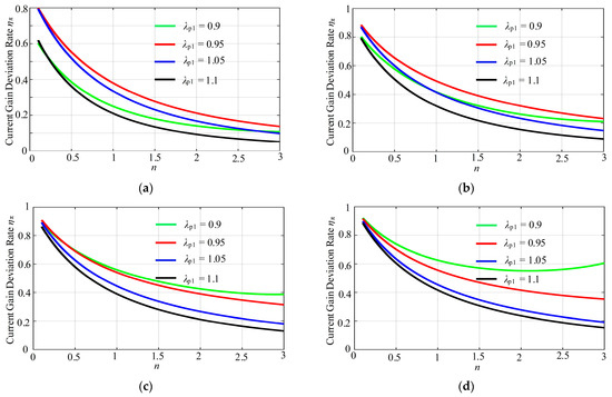
Figure 5.
The output current deviation rate under different λp1 and Qπ. (a) Qπ = 0.2; (b) Qπ = 0.4; (c) Qπ = 0.8; (d) Qπ = 1.6.
Further, it can be noted from (8) and (15) that the variation in the load R′L can be equated to the fluctuation of Qπ. The comparison of Figure 5c,d indicates that when Qπ = 0.8 and Qπ = 1.6, the deviation ηπ of the output current remains basically the same at the capacitance ratio n < 0.5, i.e., the load-independent output characteristics can still be implemented. However, from Figure 5a,b, when Qπ = 0.2 and Qπ = 0.4, the deviation ηπ of the output current fluctuates significantly at n < 0.5. This suggests that a larger Qπ in the load range is better. From (6) and (15), an increase in Qπ can be achieved by decreasing the capacitance ratio n without changing the resonant frequency and equivalent load of the system. Therefore, for the π-circuit, lowering the capacitance ratio n not only reduces the effect of the parametric deviation on the load-independent constant current, but also reduces the fluctuation of the output current.
Furthermore, the analysis of (15) reveals that the parametric deviation of the compensation capacitors C2 and Cs2 lead to fluctuations in the capacitance ratio. Thus, the fluctuation range D of the capacitance ratio can be further represented as
where a1 and b1 are the ratios of the actual to ideal values for the compensation capacitors C2 and Cs2.
From (18), when parameter deviations of compensation capacitors are Cs2 and C2, i.e., a1, b1 ∈ [0.9, 1.1], the fluctuation range is D ∈ (0.82, 1.22). From Figure 5, when λp1 ≠ 1, the smaller the capacitance ratio n, the smaller the output current deviation ηπ under D ∈ (0.82, 1.22). Consequently, at the low capacitance ratio, capacitance ratio fluctuations caused by the parametric deviation of compensation capacitors Cs2 and C2 have little effect on the load-independent output characteristics.
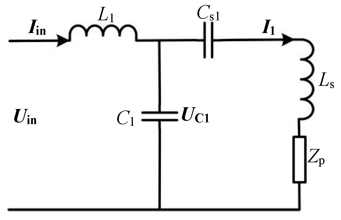
Then, in order to analyze the load-independent constant output characteristics of the L-circuit under the parametric deviation, Figure 2 can be further equated to Figure 6, where equivalent impedance Zp of the secondary side can be expressed as (19).

Figure 6.
The equivalent model for the parameter sensitivity analysis of L-circuit.
From Figure 6, the output current I1 and output voltage Uc1 of the L-circuit can be expressed as (20) and (21).
where
From (20), if compensating elements L1 and C1 are designed to satisfy the condition in (6), the current I1 remains constant and is unaffected by variations in the equivalent load ZL-L of the L-circuit. Similarly, the ±10% parametric deviation in the compensating elements L1 and C1 inevitably leads to λ1 ≠ 1, and the loss of the load-independent constant output characteristics.
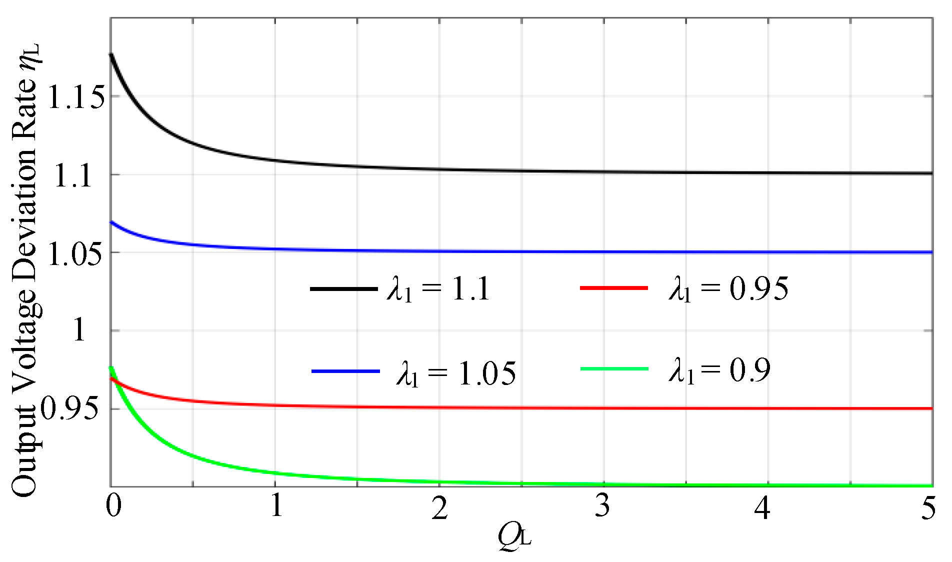
To still maintain the load-independent constant output characteristics of the L-circuit, from (21), the output voltage deviation rate ηL = |Uc1(λ1≠1)|/|Uc1(λ1 = 1)| as the function of QL can be shown in Figure 7 under different λ1. As illustrated in Figure 7, the deviation rate ηL remains essentially constant over the larger range of QL. Consequently, QL should be designed to be as large as possible during the load RL range.
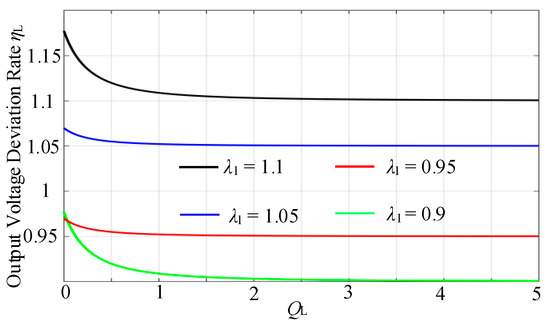
Figure 7.
The output voltage deviation rate under different λ1.
In order to investigate the method for increasing QL, through the parameter optimization, based on (6), (19), and (22), it can be further denoted as
From (23), the reduction in the capacitance ratio n can not only lead to an increase in QL at the same load R′L but also reduce the fluctuation in QL caused by load variations. This means that QL remains almost constant over the load range. As a result, the load-independent constant output of L-circuit can be equivalently implemented by reducing the capacitance ratio.
Based on the above analysis, it can be concluded that reducing the capacitance ratio can enable the DS-LCC compensation network to maintain the load-independent constant output characteristics under the parametric deviation of the compensation element. However, from [23], when the rectifier is not operated in continuous mode, the system could still lose the load-independent constant output. Therefore, the boundary condition between the continuous and discontinuous mode needs to be derived and always keep the rectifier in the continuous mode under the parametric deviation.
The load current IR depends on the average value of the current i0 and can be expressed as (24).
For the rectifier, the voltage UC2 should be greater than the load voltage UR for operation in the continuous mode. Therefore, based on (24) and (25), the boundary condition for the continuous mode can be deduced as
It can be observed from (27) that the compensation inductance L2 should be slightly larger than the ideal value to ensure that the rectifier operates in the continuous mode.
From (4) and (7), the parametric deviation not only affects the load-independent constant output characteristics, but also cause fluctuations in the transmission gain g. Based on (14) and Figure 5, under the parametric deviation, the current gain of the π-circuit can be maintained as a constant also through reducing the capacitance ratio. However, according to (20), for the L-circuit, the current I1 fluctuations caused by the parametric deviation are unavoidable. Hence, the conventional FM control can be adopted to achieve the constant current I1, and the current I1 can be further deduced as
where a1 and b1 are the deviation coefficients of L1 and C1, and can be denoted as
It can be observed from (28) that under the parametric deviation of L1 and C1, the constant output current I1 can be achieved by the FM control.
2.2. Implementation of the Soft Switching
For an IPT system, it is essential to implement the soft switching over the load range to improve efficiency. Since the IPT system generally operates at a higher frequency, the inverter is generally composed of MOSFETs. Hence, ZVS is more conducive to minimizing losses than the zero current switching. For the MOSFET, if the turn-off current Ioff satisfies the condition in (30), ZVS can be implemented [24].
where Cj and td denote the junction capacitance and dead time.
For an IPT system, the imaginary part of the input impedance is required to be greater than zero for implementing ZVS. Therefore, on the basis of (2) and (6), the input impedance of the system can be deduced as
where
It can be observed from (31) that the parametric deviation of the compensation elements L2, C2, C1, and Cs1 may cause the imaginary part of the input impedance to be less than zero. However, from (6) and (15), with the constant resonant frequency, the compensation capacitance C2 decreases with the reduction in the capacitance ratio. Based on (32), the smaller the compensation capacitor C2 is, the smaller the impedance fluctuation caused by the parametric deviation of compensation elements L2 and C2.
Moreover, based on the above analysis of the L-circuit, FM control is employed to achieve the constant current I1. From (28), the impedance fluctuation of compensation capacitor C1 is small with the FM. Therefore, the parametric deviation of Cs1 should be the primary consideration to ensure the realization of ZVS.
In order to investigate the design constraints of the compensation capacitor Cs1, the input current should be further investigated. From (31), the fundamental harmonic Iin-1st of the input current can be expressed as
In addition, L1 and C1 compose an LC filter on the primary side, which causes the input current to contain high harmonic currents. The (2m + 1)th harmonics Iin-(2m+1)th of the input current can be expressed as
Further, the input current for all higher harmonics can be derived as (35).
Based on (30) and (35), under the ±10% parametric deviation, for the realization of ZVS, the compensation capacitor Cs1 should satisfy the condition in (36).
3. Design of the DS-LCC Compensated IPT Converter with the Proposed Method
3.1. Design Procedure with Proposed Method
On the basis of the above analysis, it can be concluded that under the parametric deviation of components, the load-independent constant current output of the DS-LCC compensation topology can be implemented by reducing the capacitance ratio n. However, the reduction in the capacitance ratio n may affect the transmission gain and transmission efficiency without the parametric deviation.
From (7), for the DS-LCC compensation topology, the transmission gain in resonance can be expressed as
Based on (37), the transmission gain g decreases as the capacitance ratio n decreases. Therefore, in order to achieve the same transmission gain at the low capacitance ratio, the compensation inductance L1 should be reduced.
From (35), the decrease in compensation inductance L1 leads to an increase in the harmonic current, and the harmonic current can be further expressed as
According to (38), with the decrease in capacitance ratio n, the harmonic current will further increase. This leads to the variation in the input impedance angle, consequently increasing the reactive power loss and switching loss of the system.
To further investigate the effect of reducing the capacitance ratio n on the system transmission efficiency, the input impedance angle α can be represented as
From (39), the input impedance angle increases as the capacitance ratio decreases, which can lead to an increase in reactive losses. Therefore, the minimum capacitance ratio nmin should be determined according to the maximum input impedance angle αmax, where the transmission efficiency can meet the requirements of the system.
Moreover, from (15), the reduction in the capacitance ratio n leads to an increase in the compensation capacitance Cs2 and a decrease in the compensation capacitance C2. However, for capacitance, the value that is too large or too small can increase the cost and difficulty of the manufacture. Therefore, the compensation capacitance Cs2 and C2 can be further expressed as
From (40), it can be seen that at a constant capacitance ratio, the compensation capacitance Cs2 and C2 can be adjusted by a reasonable choice of the resonant frequency, thus, reducing the cost of the system.
On the basis of the above analysis, it can be concluded that under the parametric deviation of components, the load-independent constant current output of the DS-LCC compensation topology can be implemented by reducing the capacitance ratio n, and the constant transmission gain can be achieved by the FM control. However, the reduction in the capacitance ratio n not only leads to a decrease in the transmission efficiency in resonance but also causes compensation capacitances Cs2 and C2 to become excessively large or small. In addition, the parasitic resistance of the compensating element is ignored in all of the above analysis, which may also affect the implementation of the load-independent constant current output. As a result, for the purpose of implementing the load-independent constant current and constant transmission gain under the parametric deviation, the proposed design approach is illustrated in Figure 8 and as follows:
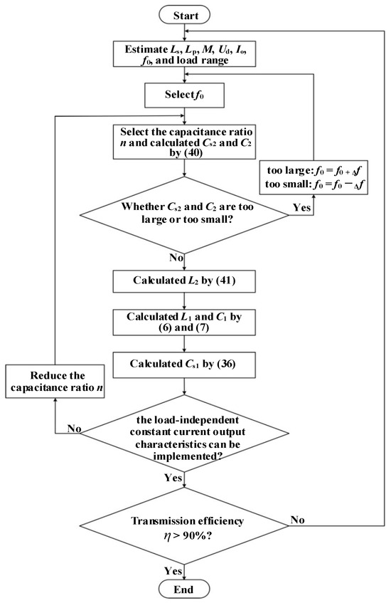
Figure 8.
The practical design procedure with the proposed method.
Step 1: Depending on the practical application, the self-inductance of the transmitter coil Ls and receiver coil Lp, mutual inductance M, input voltage Ud, output current Io, resonant frequency f0, and load range must be estimated.
Step 2: According to the ±10% parameter fluctuation, the capacitance ratio n can be selected. Furthermore, according to the receiver coil Lp, resonant frequency f0, and capacitance ratio nc, the compensation capacitance Cs2 and C2 can be calculated by (40).
Step 3: At this point, in order to reduce the cost and manufacturing difficulty of the system, Cs2 and C2 should be checked to see whether they are too large or too small. If Cs2 or C2 is too large, the resonant frequency f0 needs to be increased, i.e., f0 = f0 + Δf0. If Cs2 or C2 is too small, the resonant frequency f0 needs to be increased, i.e., f0 = f0 − Δf0.
Step 4: In accordance with (27), the larger the compensation inductance L2 is, the easier the rectifier operates in the continuous mode. However, a large L2 could increase the size of the receiving LCC network, which is not conducive to the lightweight design of the receiving side. Therefore, the minimum compensation inductance L2 for the continuous mode operation of the rectifier should be designed according to the load and ±10% parameter fluctuation range and can be calculated by (41).
Step 5: At this point, to meet the transmission gain of the system, based on the input voltage Ud, output current Io, mutual inductance M, and resonant frequency f0, the compensation inductance L1 and the compensation capacitance C1 can be calculated by (6) and (7).
Step 6: With the purpose of implementing the ZVS, the compensation capacitance Cs1 can be calculated by (36).
Step 7: At this time, within the FM range and ±10% parametric deviation, the load-independent constant current output characteristics can be implemented. If the results are not satisfied, reduce the compensation capacitance ratio n and recalculate the parameter of this compensation topology.
Step 8: Based on the above analysis, decreasing the capacitance ratio can lead to an increase in the harmonic current, and result in a decrease in the transmission efficiency of the system. For the IPT system, the transmission efficiency η = URIR/UdId should be greater than 90% according to [25,26,27]. Therefore, it is necessary to verify whether η > 90%. If the efficiency is not achieved, the entire parametric design process needs to be repeated.
3.2. Design of the Proposed IPT System
When the design of the compensation network is completed, the proposed IPT system still requires the FM to achieve the constant current output. Consequently, the schematic diagram of the DS-LCC compensation IPT converter can be represented as in Figure 9. As can be gathered from Figure 9, the output current I1 of the L-circuit is detected and conveyed to the FM controller. Then, switching signals can be generated by comparing I1 with Iref. This demonstrates that the suggested methodology is able to eliminate the communication module between the transmitter and receiver.
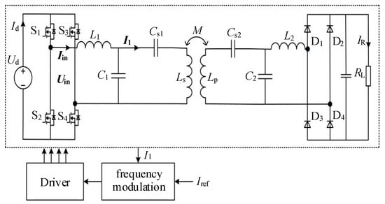
Figure 9.
Schematic diagram of the proposed IPT system.
4. Experimental and Simulation Verification
Based on the preceding analysis, it is evident that the DS-LCC compensation topology can maintain the load-independent constant current output despite the parametric deviation of components by decreasing the capacitance ratio n. Additionally, the constant transmission gain can be attained through the FM control. In order to validate the effectiveness and feasibility of the proposed method, under the same electrical parameters illustrated in Table 1, the parameters of the DS-LCC compensation network with the capacitance ratio n = 1 shown in Table 2 are optimized. According to the parameter design procedure illustrated in Figure 8, the optimization result is shown in Table 3, in which the capacitance ratio n = 0.15.

Table 1.
Electrical parameter.
Table 2.
Parameters of the double-sided LCC compensation network at n = 1.
Table 3.
Parameters of the double-sided LCC compensation network at n = 0.15.
4.1. Simulation Verification
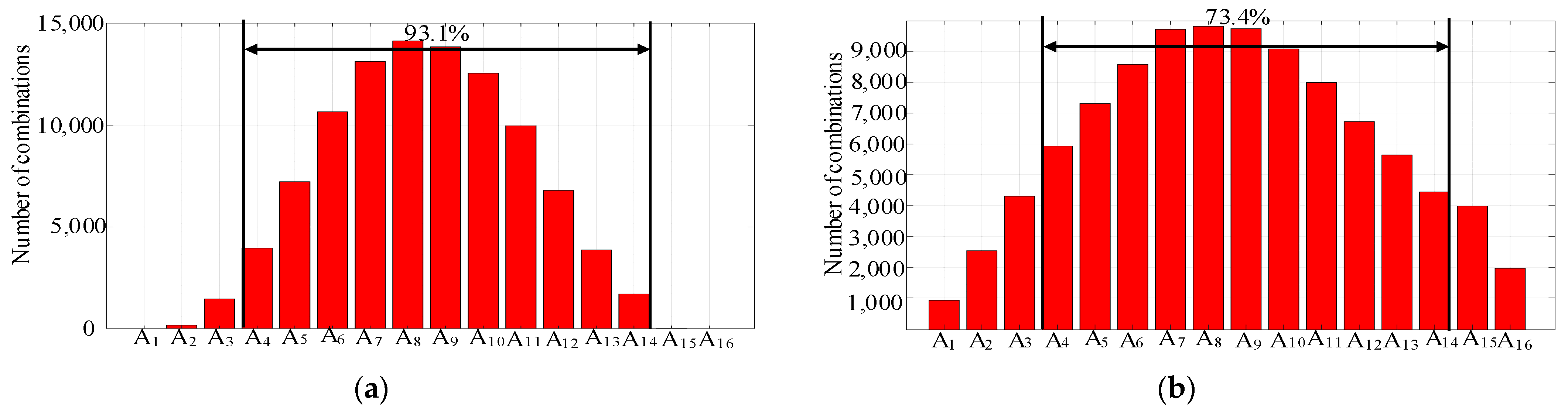
In practice, for the DS-LCC compensation network, it is often the case that the parametric deviation of multiple components exists simultaneously. Therefore, in order to validate the effectiveness of the proposed method, a random numerical statistical simulation based on the Monte Carlo analysis is further adopted. Within the ±10% parametric deviation range and an accuracy of 0.0001, 100,000 combinations of random parametric deviation are generated through MATLAB 2018b under n = 0.15 and n = 1, respectively. In this paper, for the convenience of counting and analyzing the influence of each combination on the output current, the output current deviation ηDS-LCC is further defined as the output current under each combination divided by the output current without the parametric deviation. Furthermore, the different ranges of the output current deviation ηDS-LCC, as indicated in Table 4, are established. Based on Table 4, the Gaussian distribution of combinations at different deviation ranges is represented in Figure 10. From Figure 10, at the capacitance ratio n = 0.15, the probability that output current deviation is within ±10% is 93.1%, while at the capacitance ratio n = 1, the probability that output current deviation is within ±10% is only 73.4%. Therefore, under the parametric deviation, the range of the output current deviation at n = 0.15 is significantly smaller than at n = 1. This means that the reduction in the capacitance ratio effectively reduces the output fluctuation, thus reducing the FM range to achieve constant transmission gain. Therefore, the parameters of the DS-LCC compensation network can be optimized by the design procedure shown in Figure 8.
Table 4.
Different deviation ranges of the output current deviation.
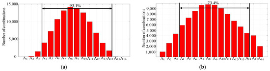
Figure 10.
Distribution of combinations at different ranges of output current deviations under different capacitance ratios n. (a) n = 0.15; (b) n = 1.
As analyzed in Section 2, for the L-circuit, the deviation factor λ1 reaches the minimum when both L1 and C1 have +10% parametric deviations, and the maximum when both L1 and C1 have −10% parametric deviations. For the π-circuit, the output characteristics can be affected by fluctuations in the capacitance ratio n and deviation factor λp1. The values of both n and λp1 would vary in the following two cases: (1) C2 has a +10% deviation while Cs2 has −10%, (2) C2 has a −10% deviation while Cs2 has +10%. Therefore, the combination of the parametric deviation shown in Table 5 is chosen for the comparative validation.
Table 5.
Parametric deviation at n = 0.15 and n = 1.
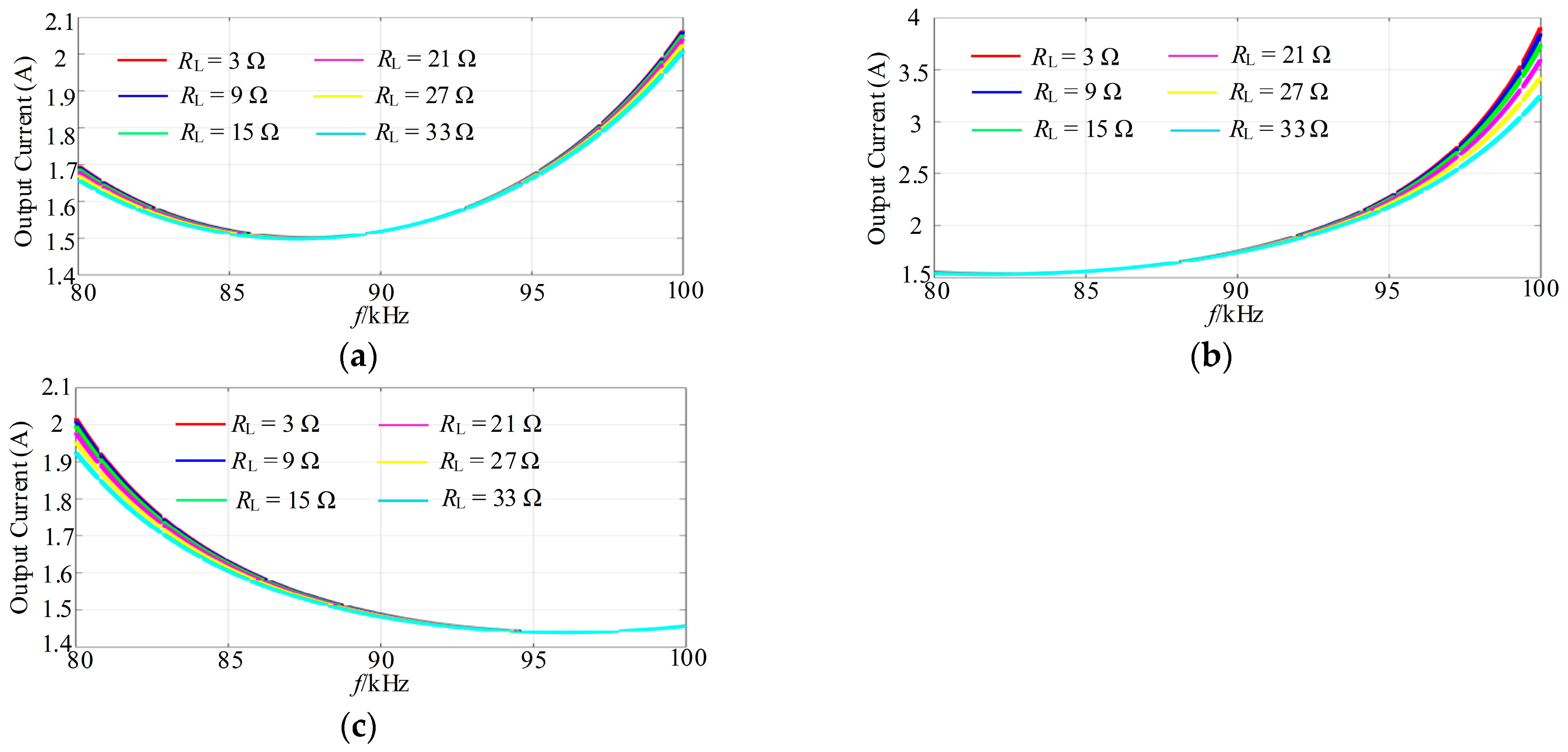
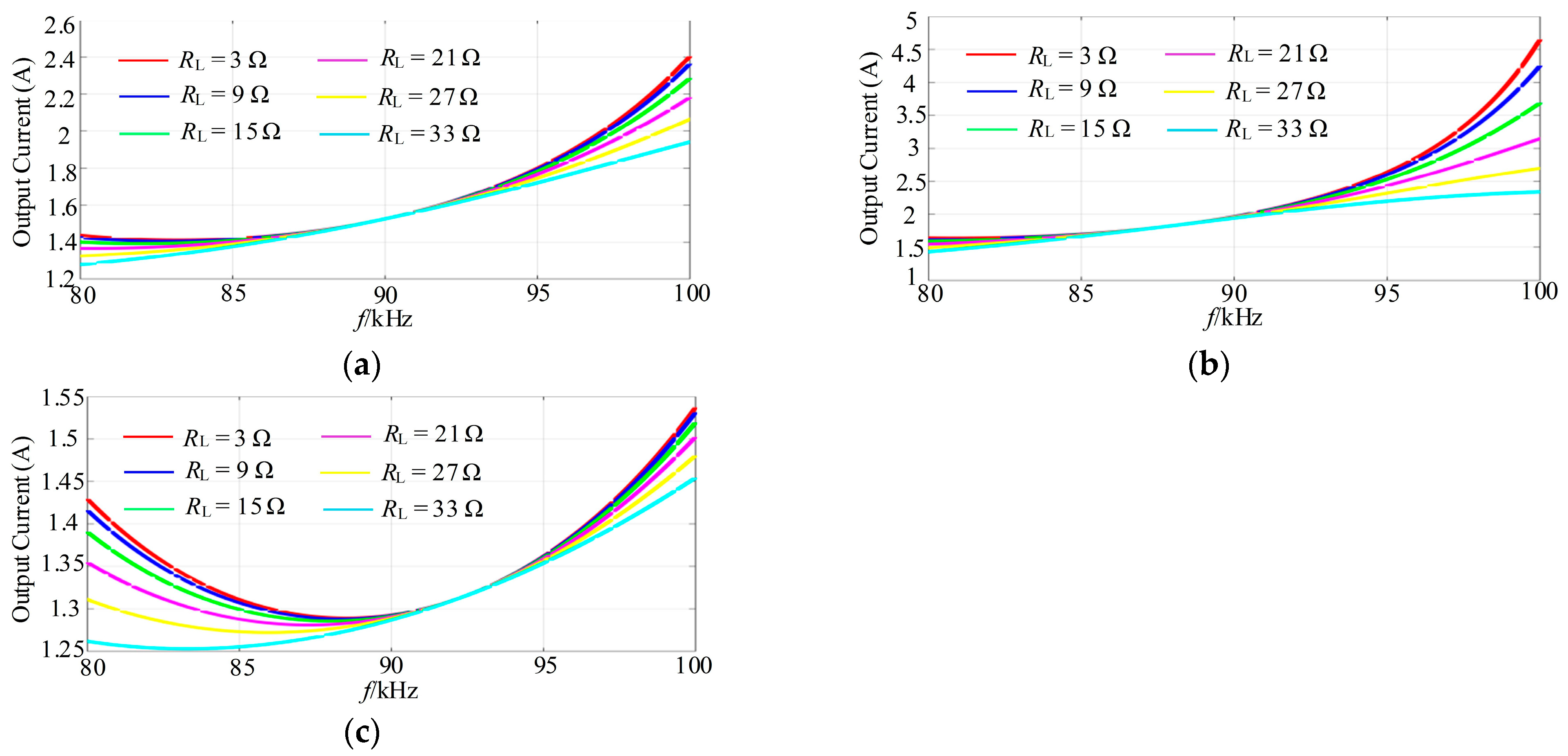
The output current, as the function of the operating frequency under different parametric deviation combinations, is represented in Figure 11 and Figure 12, when n = 0.15 and n = 1. From Figure 11a and Figure 12a, without the parametric deviation, the FM range for implementing the load-independent constant current output characteristics is 85 kHz to 95 kHz for n = 0.15, while the FM range is only 88 to 92 kHz for n = 1. Likewise, it can be observed from the comparison of Figure 11b and Figure 12b that when the parametric deviation is Case 1, the FM range with the load-independent constant output is 80 kHz to 92 kHz for n = 0.15, and the FM range is 85 kHz to 90 kHz for n = 1. From Figure 11c and Figure 12c, when the parametric deviation is Case 2, the FM range for n = 0.15 is also wider than that for n = 1. Therefore, through the reduction in the capacitance ratio n, the load-independent constant output characteristics can be maintained under the parametric deviation and FM.
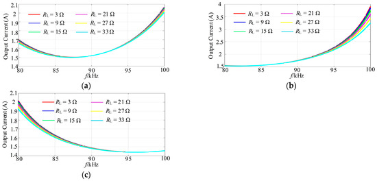
Figure 11.
The output current under different loads and parametric deviation combinations when n = 0.15. (a) Without the parameter fluctuation; (b) Case 1; (c) Case 2.
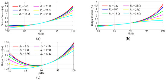
Figure 12.
The output current under different loads and parametric deviation combinations when n = 1. (a) Without the parameter fluctuation; (b) Case 1; (c) Case 2.
4.2. Experimental Verification
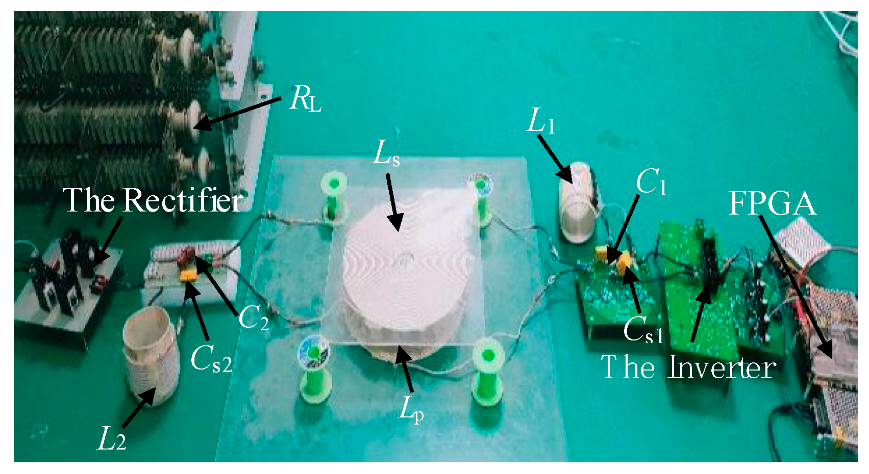
Based on Table 1, Table 2 and Table 4, a prototype of the DS-LCC compensation topology is shown in Figure 13. The main DC-AC full-bridge inverter comprises four MOSFETs with the manufacturer part number SPW47N60C3, and the secondary rectifier comprises four fast-recovery diodes with manufacturer part number MUR860T. The main electrical parameters of the MOSFET and fast recovery diode are shown in Table 6. The load is substituted by a variable resistor. Coupling coils are designed as the conventional round.
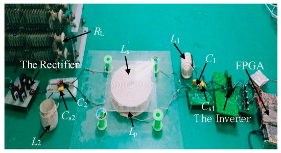
Figure 13.
Experimental platform for the DS-LCC IPT converter.
Table 6.
Main electrical parameters of the MOSFET and fast recovery diode.
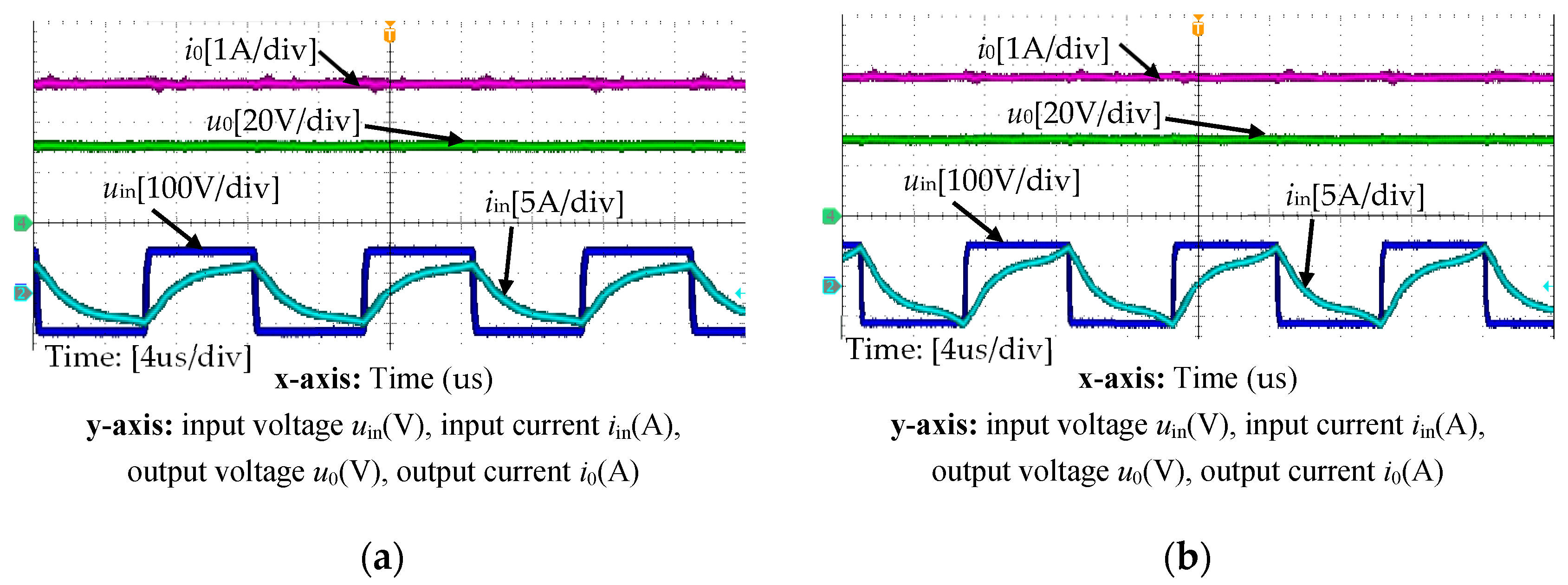
Without the parametric deviation, experimental waveforms of input current iin, input voltage uin, load current iR, and load voltage uR under different loads and capacitance ratios are shown in Figure 14. It can be observed from Figure 14 that regardless of n = 0.15 or n = 1, the load current is almost constant at 1.5 A at 90 kHZ when the load is increased from 3 Ω to 33 Ω. This indicates that without the parametric deviation, the load-independent constant output characteristics can be maintained at different capacitance ratios. Moreover, ZVS can be implemented over the load range at different capacitance ratios. When RL = 33 Ω, i.e., at the rated output power, the efficiency is 93.5% and 94.2% for n = 0.15 and n = 1, respectively. Based on (37), to obtain the same transmission gain under different capacitance ratios, a smaller compensating inductance L1 is required at the lower capacitance ratio. From (38), the harmonic input current would be increased at the smaller L1. Therefore, it can be noticed that the efficiency with the capacitance ratio n = 0.15 is slightly lower than that with the capacitance ratio n = 1.
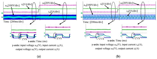
Figure 14.
Experimental waveforms under different loads and capacitance ratios without parametric deviation. (a) n = 1; (b) n = 0.15.
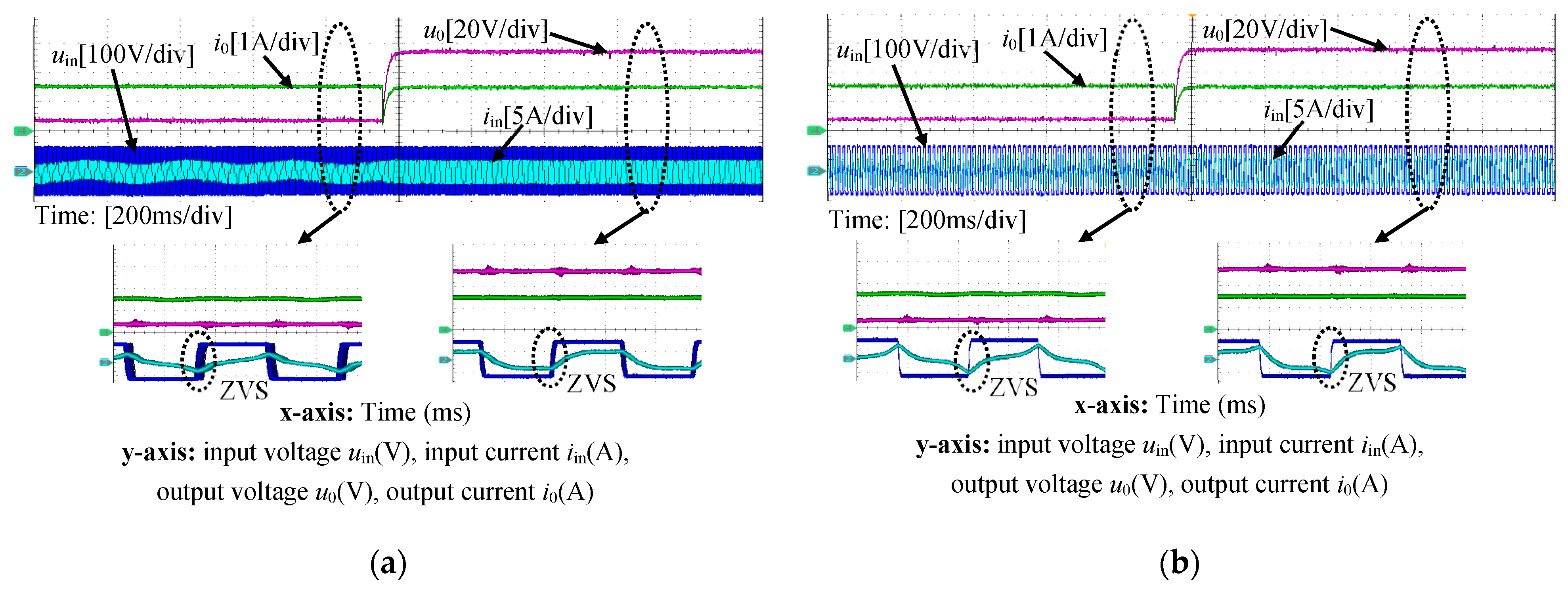
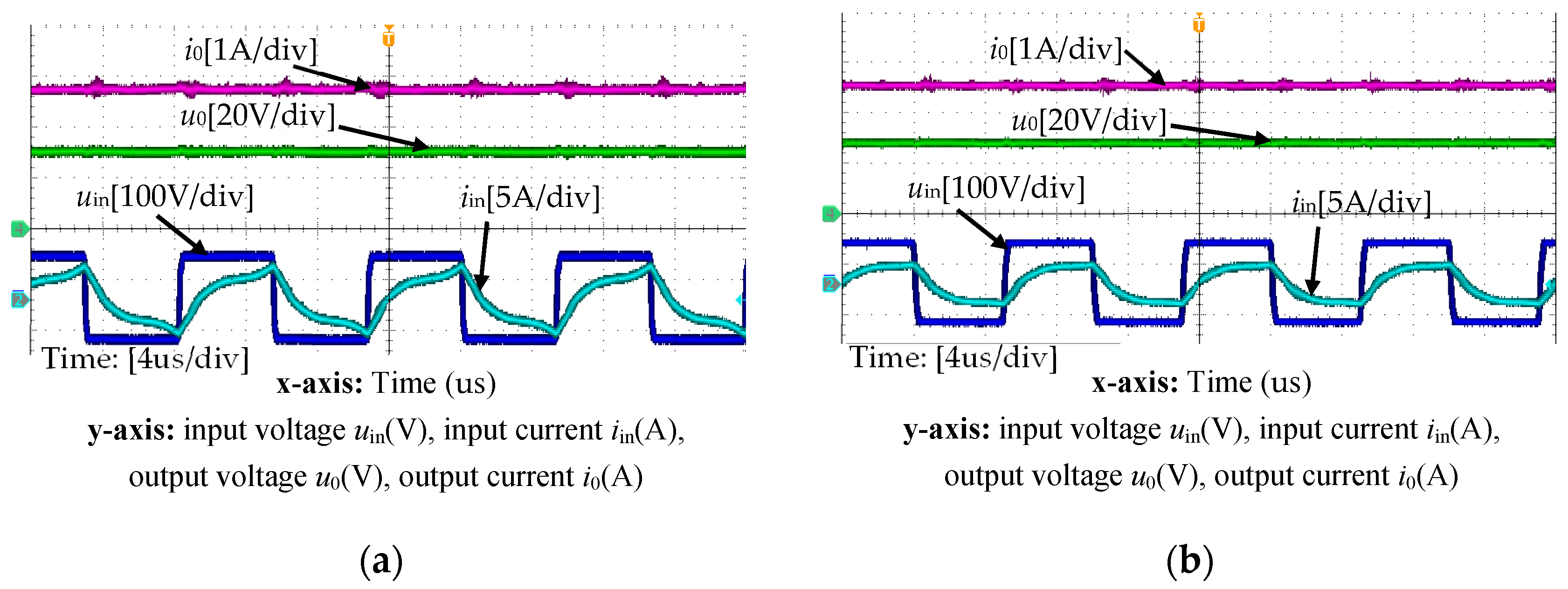
Figure 15 illustrates experimental waveforms of input current iin, input voltage uin, load current iR, and load voltage uR under different capacitance ratio when the parametric deviation is Case 1 and RL = 33 Ω. It can be observed from Figure 15a that when n = 1, the output current can be sustained at 1.5 A by adjusting the operating frequency from 90 kHz to 80 kHz. According to Figure 15b, when n = 0.15, the operating frequency only needs to be regulated from 90 kHz to 85 kHz to maintain the output current at 1.5 A. Due to the increase in the reactive power caused by the FM, the efficiency at n = 1 and n = 0.15 drops to 73.9% and 87.4%. A comparison of Figure 15a,b shows that the higher efficiency can be obtained at n = 0.15, since the FM range is smaller.
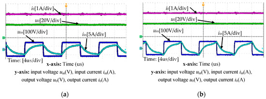
Figure 15.
Experimental waveforms under different capacitance ratios when the parametric deviation is Case 1 and RL = 33 Ω. (a) n = 1; (b) n = 0.15.
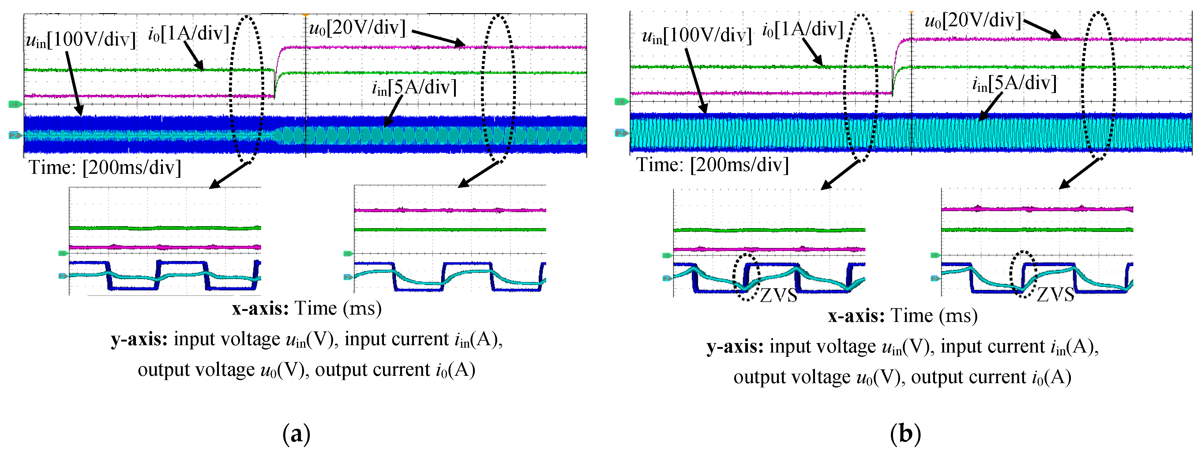
Figure 16 demonstrates the experimental waveforms of load switching under different capacitance ratios when the parametric deviation is Case 1. Based on Figure 16a, under n = 1, when the load is changed from 3 Ω to 33 Ω, the output current varies from 1.77 A to 1.5 A, and the fluctuation of the output current is +18%. This indicates that the load-independent constant current characteristic at n = 1 is lost. From Figure 16b, under n = 0.15, the output current is briefly lowered and remains at 1.52 A after 40 ms. The maximum fluctuation of the output current is only +3.33%. Comparing Figure 16a,b, when the parametric deviation is Case 1, the load-independent constant current characteristic can also be realized at n = 0.15. Moreover, at n = 0.15, ZVS can be implemented over the load range.
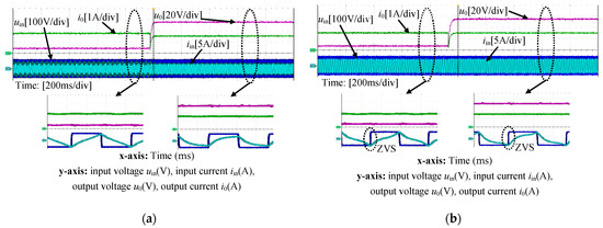
Figure 16.
The experimental waveforms of load switching under different capacitance ratios when the parameter deviation is Case 1. (a) n = 1; (b) n = 0.15.
Figure 17 illustrates experimental waveforms of input current iin, input voltage uin, load current iR, and load voltage uR under different capacitance ratio when the parametric deviation is Case 2 and RL = 33 Ω. As can be noticed from Figure 17a, when n = 1, the output current can be sustained at 1.5 A by adjusting the operating frequency to 100 kHz. Based on Figure 17b, when n = 0.15, the operating frequency only needs to be regulated to 95 kHz to maintain the output current at 1.5 A. Similarly, because of the smaller FM range, the transmission efficiency is higher at 84.9% for n = 0.15, while it is lower at 68.2% for n = 1.
Figure 17.
Experimental waveforms under different capacitance ratios when the parametric deviation is Case 2 and RL = 33 Ω. (a) n = 1; (b) n = 0.15.
Figure 18 shows the experimental waveforms of load switching under different capacitance ratios when the parametric deviation is Case 2. Based on Figure 18a, under n = 1, when the load is changed from 3 Ω to 33 Ω, the output current varies from 1.47 A to 1.61 A at the constant operating frequency, the fluctuation of the output current is +7.3%. From Figure 18b, under n = 0.15, the output current can also be maintained at approximately 1.5 A within 40 ms, and the fluctuation is less than 5%. Likewise, from Figure 18, when the parametric deviation is Case 2, the load-independent constant current characteristic can also be realized under n = 0.15. In addition, at n = 0.15, ZVS can also be implemented over the load range.

Figure 18.
The experimental waveforms of load switching under different capacitance ratios when the parameter deviation is Case 2. (a) n = 1; (b) n = 0.15.
It can be observed from Table 7 that, compared with the previous methods, under multi-parametric deviation of the DS-LCC compensation network, load-independent constant-current output characteristics and constant transmission gain can be implemented through the suggested method. Compared to the methods presented in [28,29], the proposed design method can achieve load-independent constant current despite the parametric deviation of the compensating inductor and compensating capacitor. Compared with [30], the proposed method does not require SCC and simplifies the control system. From [19,20], the influence of parameter deviations can be minimized under the rated power, which means that the load-independent constant current output characteristics cannot be realized. With the proposed method, the load-independent constant current output can be maintained over the 10–100% of the rated output power.
Table 7.
Comparison with the previous method.
5. Conclusions
From the experimental results, the maximum fluctuation of the output current at n = 0.15 is +3.33%, while that at n = 1 is +18%. This means that through reducing the capacitance ratio n, the load-independent constant output characteristics of the DS-LCC compensation topology can be maintained under the ±10% parametric deviation. Moreover, the constant transmission gain can be realized by FM. The frequency modulation range is 85 kHz–95 kHz at n = 0.15, while that is 80 kHz–100 kHz at n = 1. The smaller the frequency adjustment range, the lower the reactive power loss caused by FM. Therefore, the transmission efficiencies at n = 0.15 are 87.4% and 84.9% under different parametric deviations, which are significantly higher than those at n = 1. Finally, reducing the capacitance ratio will lead to an increase in the harmonic content of the input current, resulting in an increase in the imaginary part of the input impedance, so further research should be carried out to reduce harmonics.
Author Contributions
Conceptualization, X.Z. and J.L.; methodology, X.Z. and J.L.; validation, X.Z. and J.L.; investigation, X.T.; writing—original draft preparation, X.Z. and J.L.; writing—review and editing, X.Z., J.L. and X.T. All authors have read and agreed to the published version of the manuscript.
Funding
This research received no external funding.
Data Availability Statement
Data are contained within the article.
Conflicts of Interest
The authors declare that they have no known competing financial interests or personal relationships that could have appeared to influence the work reported in this paper.
References
- Cai, J.; Sun, P.; Ji, K.; Wu, X.; Ji, H.; Wang, Y.; Rong, E. Constant-Voltage and Constant-Current Controls of the Inductive Power Transfer System for Electric Vehicles Based on Full-Bridge Synchronous Rectification. Electronics 2024, 13, 1686. [Google Scholar] [CrossRef]
- Shen, H.; Wang, X.; Sun, P.; Wang, L.; Liang, Y. Mutual Inductance and Load Identification of LCC-S IPT System Considering Equivalent Inductance of Rectifier Load. Electronics 2023, 12, 3841. [Google Scholar] [CrossRef]
- Luo, S.; Yao, Z.; Zhang, Z.; Li, G.; Zhang, X.; Ma, H. A Dual Shunt Inductor Compensated IPT System with Nearly Unity Power Factor for Wide Load Range and Misalignment Tolerance. IEEE Trans. Ind. Electron. 2022, 69, 10001–10013. [Google Scholar] [CrossRef]
- Luo, S.; Yao, Z.; Zhang, Z.; Zhang, X.; Ma, H. Balanced Dual-Side LCC Compensation in IPT Systems Implementing Unity Power Factor for Wide Load Range and Misalignment Tolerance. IEEE Trans. Ind. Electron. 2023, 70, 7796–7809. [Google Scholar] [CrossRef]
- Li, J.; Zhang, X.; Tong, X. Research and Design of Misalignment-Tolerant LCC–LCC Compensated IPT System with Constant-Current and Constant-Voltage Output. IEEE Trans. Power Electron. 2023, 38, 1301–1313. [Google Scholar] [CrossRef]
- Rezazade, S.; Shahirinia, A.; Naghash, R.; Rasekh, N. A Novel Efficient Hybrid Compensation Topology for Wireless Power Transfer. IEEE Trans. Ind. Electron. 2023, 70, 2277–2285. [Google Scholar] [CrossRef]
- Zhang, X.; Zheng, H.; Xu, F.; Chen, Z. Accurate Modeling of Discontinuous Operating State for LCC-LCC Compensated Inductive Power Transfer Converters by Time-Domain-Analysis. IEEE J. Emerg. Sel. Top. Power Electron. 2024. [Google Scholar] [CrossRef]
- Cai, J.; Wu, X.; Sun, P.; Deng, Q.; Sun, J.; Zhou, H. Design of Constant-Voltage and Constant-Current Output Modes of Double-Sided LCC Inductive Power Transfer System for Variable Coupling Conditions. IEEE Trans. Power Electron. 2024, 39, 1676–1689. [Google Scholar] [CrossRef]
- Huang, C.-Y.; James, J.E.; Covic, G. A Design Considerations for Variable Coupling Lumped Coil Systems. IEEE Trans. Power Electron. 2015, 30, 680–689. [Google Scholar] [CrossRef]
- Zhang, Z.; Zheng, S.; Luo, S.; Xu, D.; Krein, P.T.; Ma, H. An Inductive Power Transfer Charging System with a Multiband Frequency Tracking Control for Misalignment Tolerance. IEEE Trans. Power Electron. 2022, 37, 11342–11355. [Google Scholar] [CrossRef]
- Rong, C.; Zhang, B. A Fractional-Order Wireless Power Transfer System with Misalignment and Detuning Tolerance. IEEE Trans. Power Electron. 2023, 38, 14884–14895. [Google Scholar] [CrossRef]
- Zhang, H.; Chen, Y.; Kim, D.-H.; Li, Z.; Zhang, M.; Li, G. Variable Inductor Control for Misalignment Tolerance and Constant Current/Voltage Charging in Inductive Power Transfer System. IEEE J. Emerg. Sel. Top. Power Electron. 2023, 11, 4563–4573. [Google Scholar] [CrossRef]
- Fu, N.; Deng, J.; Wang, Z.; Chen, D. An LCC–LCC Compensated WPT System With Switch-Controlled Capacitor for Improving Efficiency at Wide Output Voltages. IEEE Trans. Power Electron. 2023, 38, 9183–9194. [Google Scholar] [CrossRef]
- Wu, L.; Zhang, B.; Jiang, Y. A Misalignment-Tolerant Autonomous Wireless Power Transfer System for Battery Charging Based on Detuning Control. IEEE Trans. Power Electron. 2024, 39, 3851–3863. [Google Scholar] [CrossRef]
- Qu, X.; Chu, H.; Wong, S.-C.; Tse, C.K. An IPT Battery Charger with Near Unity Power Factor and Load-Independent Constant Output Combating Design Constraints of Input Voltage and Transformer Parameters. IEEE Trans. Power Electron. 2019, 34, 7719–7727. [Google Scholar] [CrossRef]
- Wang, D.; Qu, X.; Yao, Y.; Yang, P. Hybrid Inductive-Power-Transfer Battery Chargers for Electric Vehicle Onboard Charging with Configurable Charging Profile. IEEE Trans. Intell. Transp. Syst. 2021, 22, 592–599. [Google Scholar] [CrossRef]
- Yang, L.; Ren, L.; Shi, Y.; Wang, M.; Geng, Z. Analysis and Design of an S/S/P-Compensated Three-Coil Structure WPT System with Constant Current and Constant Voltage Output. IEEE J. Emerg. Sel. Top. Power Electron. 2023, 11, 2487–2500. [Google Scholar] [CrossRef]
- Hou, X.; Hu, H.; Su, Y.; Liu, Z.; Deng, Z.; Deng, R. A Multirelay Wireless Power Transfer System with Double-Sided LCC Compensation Network for Online Monitoring Equipment. IEEE J. Emerg. Sel. Top. Power Electron. 2023, 11, 1262–1271. [Google Scholar] [CrossRef]
- Wang, Y.; Mostafa, A.; Zhang, H.; Mei, Y.; Zhu, C.; Lu, F. Sensitivity Investigation and Mitigation on Power and Efficiency to Resonant Parameters in an LCC Network for Inductive Power Transfer. IEEE J. Emerg. Sel. Top. Power Electron. 2022, 3, 443–453. [Google Scholar] [CrossRef]
- Wang, Y.; Yang, Z.; Lin, F.; Dong, J.; Bauer, P. Frequency Tracking Method and Compensation Parameters Optimization to Improve Capacitor Deviation Tolerance of the Wireless Power Transfer System. IEEE Trans. Ind. Electron. 2023, 70, 12244–12253. [Google Scholar] [CrossRef]
- Wang, X.; He, R.; Wang, H.; Liang, J.; Fu, M. Modified LCC Compensation and Magnetic Integration for Inductive Power Transfer. IEEE J. Emerg. Sel. Top. Power Electron. 2024, 12, 186–194. [Google Scholar] [CrossRef]
- Zhang, X.; Xue, R.; Wang, F.; Xu, F.; Chen, T.; Chen, Z. Capacitor Tuning of LCC-LCC Compensated IPT System with Constant-Power Output and Large Misalignments Tolerance for Electric Vehicles. IEEE Trans. Power Electron. 2023, 38, 11928–11939. [Google Scholar] [CrossRef]
- Li, W.; Zhang, Q.; Li, H.; Cui, C.; Wei, G. Series Filter Computational Method for CCM Recovery in Double Side LCC WPT System. IEEE Trans. Ind. Electron. 2022, 69, 8875–8882. [Google Scholar] [CrossRef]
- Cai, J.; Wu, X.; Sun, P.; Deng, Q.; Sun, J.; Zhou, H.; Wang, X. Zero-Voltage Switching Regulation Strategy of Full-Bridge Inverter of Inductive Power Transfer System Decoupled from Output Characteristics. IEEE Trans. Power Electron. 2022, 37, 13861–13873. [Google Scholar] [CrossRef]
- Lu, J.; Zhu, G.; Lin, D.; Zhang, Y.; Jiang, J.; Mi, C.C. Unified Load-Independent ZPA Analysis and Design in CC and CV Modes of Higher Order Resonant Circuits for WPT Systems. IEEE Trans. Transport. Electrif. 2019, 5, 977–987. [Google Scholar] [CrossRef]
- Casaucao, I.; Triviño, A.; Corti, F.; Reatti, A. SS and LCC–LCC in Simultaneous Wireless Power and Data Transfer: A Comparative Analysis for SAE J2954-Compliant EVs. IEEE Trans. Ind. Inform. 2024, 20, 8195–8206. [Google Scholar] [CrossRef]
- Wang, V.; Thrimawithana, J.; Neuburger, M. An Si MOSFET-Based High-Power Wireless EV Charger With a Wide ZVS Operating Range. IEEE Trans. Power Electron. 2021, 36, 11163–11173. [Google Scholar] [CrossRef]
- Chen, Y.; Wu, J.; Zhang, H.; Guo, L.; Lu, F.; Jin, N.; Kim, D.-H. A Parameter Tuning Method for a Double-Sided Compensated IPT System with Constant-Voltage Output and Efficiency Optimization. IEEE Trans. Power Electron. 2023, 38, 4124–4139. [Google Scholar] [CrossRef]
- Lu, J.; Zhu, G.; Wang, H.; Lu, F.; Jiang, J.; Mi, C.C. Sensitivity Analysis of Inductive Power Transfer Systems with Voltage-Fed Compensation Topologies. IEEE Trans. Veh. Technol. 2019, 68, 4502–4513. [Google Scholar] [CrossRef]
- Tan, P.; Song, B.; Lei, W.; Yin, H.; Zhang, B. Decoupling Control of Double-Side Frequency Tuning for LCC/S WPT System. IEEE Trans. Ind. Electron. 2023, 70, 11163–11173. [Google Scholar] [CrossRef]


Disclaimer/Publisher’s Note: The statements, opinions and data contained in all publications are solely those of the individual author(s) and contributor(s) and not of MDPI and/or the editor(s). MDPI and/or the editor(s) disclaim responsibility for any injury to people or property resulting from any ideas, methods, instructions or products referred to in the content. |
© 2025 by the authors. Licensee MDPI, Basel, Switzerland. This article is an open access article distributed under the terms and conditions of the Creative Commons Attribution (CC BY) license (https://creativecommons.org/licenses/by/4.0/).