This section describes the structure and functionality of an APUF (Arbiter PUF). It discusses the challenges associated with implementing APUFs on FPGAs and presents their characteristics as well as optimizations to improve performance and resource utilization. In addition, current approaches and solutions for various APUF implementations from recent research are presented and analyzed in detail. Finally, the use of PUFs for enhancing the security of a device is also briefly described in this section.
2.1. Delay-Based Physical Unclonable Functions
Delay-based PUFs generate device-specific signals that can be used in various security applications. Here, the propagation delay of two identical circuits that differ in processing time due to variations in the manufacturing process, aging effects, or internal and external influences are analyzed. In contrast to ring oscillator PUFs (RO-PUF) [
19,
20,
21], APUFs generate unique output signals by passing a trigger signal through parallel paths and analyzing which path has the fastest propagation delay (
Figure 1a). The path can be changed by the challenge bits
c, which modify the routing of the path and thus impact propagation delay. Path changes are performed by switching units (SUs), which consist of two multiplexers (MUXs) as shown in
Figure 1a. At the end of an APUF chain, a register (FF) is used to generate the response bit. In this case, a ‘1’ is generated if the signal at the D input arrives before the signal at the C (CLK) input, while a ‘0’ is generated when the signal at the C input arrives first. In the following, a series of SUs is referred to as an arbiter block.
A major disadvantage of this APUF is that a complete symmetrical implementation of the paths on FPGAs is extremely difficult or even impossible due to their specific and fixed architecture. The main problem arises from asymmetries in the connection of two SUs, which are caused by other FPGA components such as digital signal processors (DSPs) or block RAMs (BRAMs), as these components enable further connections and thus disrupt the routing of an arbiter chain. In addition, the parallel routing of two paths through a switching matrix is either very difficult or not feasible due to the fixed routing options. An additional asymmetry arises at the connection between the last SU and the register responsible for generating a response bit, as the routing to the D and C inputs of the register cannot be done symmetrically. However, this offset can be minimized through targeted routing adjustments, which help reduce the negative impact on the generation of the response bit. Furthermore, the uneven distribution of FPGA components, such as DSBs, BRAMs, and others, can cause fixed offsets in propagation delay that are uniform across all individual FPGA devices of the same type. This uneven architecture can affect the randomness and uniqueness of the output signal [
11]. As described in our previous works [
11,
18,
22], conventional APUFs as in [
23,
24] show high reliability and low uniqueness, which can be attributed to an asymmetric design strategy. These PUFs are therefore not suitable for use in security applications. For this reason, the implementation of the APUF in
Figure 1a is better suited for ASICs (Application-Specific Integrated Circuits).
To reduce offsets in propagation delay, the paths are implemented in two separate arbiter blocks as shown in
Figure 1b. By using the same challenge bits for the respective SUs of the two arbiter blocks, the paths (red and blue) can be implemented in parallel, resulting in a DAPUF block. Due to the two-dimensional structure of FPGAs, an arbiter block consists of a chain of CLBs (Configurable Logic Blocks) connected in series. For the symmetry, the second arbiter block is implemented with the same routing configuration (e.g., through the hard macro function) under the first arbiter block, so that the SUs in each stage (
) are implemented directly below one another. Due to the identical routing configuration and the identical structure of the CLBs within an FPGA, symmetrical paths can be established between two arbiter blocks. This approach enables the implementability of APUFs on FPGAs by using specific constraints or the hard macro function of the EDA tool. For this purpose, it should be noted that the chain of CLBs should not be disturbed by other FPGA components. Therefore, resource efficiency and reducing SU-SU connections are essential, as further described in
Section 5 in detail. This extended PUF structure is called 2-1 double arbiter PUF (2-1 DAPUF), as a single response bit is generated for two arbiter blocks. Due to this optimization, DAPUFs as in [
25,
26] show improved uniqueness compared to APUFs. The disadvantage of this structure is that it features double the number of arbiter blocks and thus hardware resources are required for the generation of a single response bit.
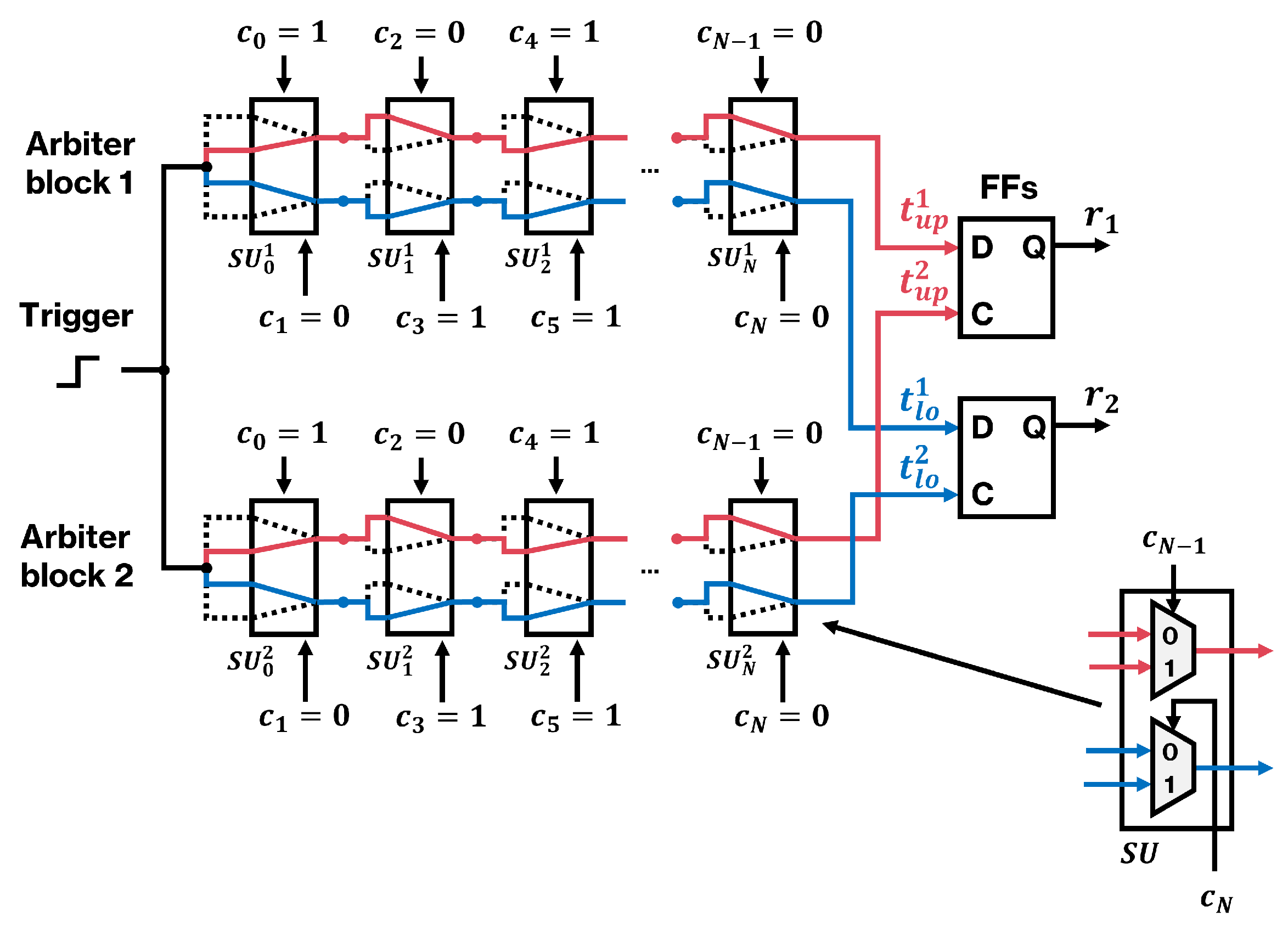
To address this problem, the structure of the 2-1 DAPUF (
Figure 1b) can be further optimized to generate individual signals with reduced resource consumption. The optimized DAPUF from our previous implementation [
22] is shown in
Figure 2. Compared to
Figure 1b, it can be observed that the arbiter blocks contain two independent paths (red and blue), each of which can be configured separately. For this purpose, the SUs include two MUXs, one for each path, and they can also be implemented into a single slice. At the output of the PUF, both paths can be evaluated independently using an FF for each response bit as shown in
Figure 2. This PUF is referred to as a 2-2 DAPUF, as two arbiter blocks are used to generate two response bits.
In [
27], a flip-flop-based APUF (FF-APUF) design on FPGAs is presented with the aim of improving the weaknesses of conventional APUFs and achieving high uniqueness (
Figure 3). The structure of this PUF is similar to the 2-1 DAPUF in
Figure 1b. The difference is that in this work, the propagation delays of FFs instead of LUTs are investigated. Therefore, an SU consists of four FFs, which are loaded with an initial value of ‘1’, and three MUXs, whereby one of four output signals of the FFs can be selected (
) by the challenge. The output signal of an SU is thus connected to the CLK signal of the subsequent SU, which is used to activate the next stage. An RS latch is then used to generate a response bit. This design was implemented on 11 FPGAs boards and tested with different ambient temperature and supply voltage variations. The average uniqueness was 41.53% and the reliability was 97.10%.
In [
28], a feed-forward XOR PUF (called FFXOR PUF) is presented. A simple feed-forward PUF is an extended version of an APUF into which one or more intermediate arbiter(s) are inserted. Instead of a direct signal race through all SUs, an intermediate arbiter captures a partial output at a specific point and uses it as additional input (as hidden challenge) for other stages. This leads to non-linearity, making the PUF more resistant to machine learning attacks, but also reduces the reliability of the responses. In order to generate a single response bit in [
28], several feed-forward PUFs are implemented in parallel, where the outputs are XORed. Therefore, two main variants are presented in this work: homogeneous FFXOR PUF, where all components have the same structure, and heterogeneous FFXOR PUF, where the components have different designs. The results from the paper show that the heterogeneous FFXOR PUF provides high security against modeling attacks. However, the designs show low reliability and are less resistant against physical influences. To solve this problem, a method called soft-response thresholding is used. Here, CRPs are generated several times to determine which challenge generates constant and stable responses. For this purpose, stable challenges can be used in security applications, while unstable challenges are discarded in this approach.
A priority arbiter PUF (called PA-PUF) is presented in [
29]. The architecture is based on a triple-input arbiter (top, center, bottom) combined with two multiplexers and XOR logic (priority arbiter). This results in a higher non-linearity compared to classic APUFs. In addition, feed-forward arbiters are integrated to increase the number of CRPs and improve security. The PA-PUF was implemented on an AMD-Xilinx Artix-7 FPGA. This design shows a randomness of 49.45% and a uniqueness of 49.63%, which are close to the ideal value of 50%. The reliability amounts to 94.5%, which is increased to 100% by using Bose–Chaudhuri–Hocquenghem (BCH) error-correcting codes (ECCs) [
30]. The architecture is also configurable so that more CRPs can be generated using an additional feed-forward arbiter.
2.2. PUF-Based Application Scenarios
One of the best-known areas of application for PUFs is PUF-based authentication protocols. The aim here is to identify attackers or unauthenticated devices in a network and to block data transmission to these devices. Authentication is basically carried out in two processes, the enrollment and the authentication phases between two nodes (device and a secure instance). In the first phase, the CPRs are exchanged. To achieve this, the server sends a random challenge to the device, receives the corresponding response, and saves the CRP in a database. In the second phase (
Figure 4a), a previously registered device is authenticated. During this process, the server fetches a CRP (
) from the database and sends the challenge to the device again. The device generates a response using the PUF (
) and sends it back to the server. The server checks whether the response received matches with the entry in the database (
). If this is the case, it can be assumed that the device has already been registered. If not, the connection is aborted. In research, PUF-based authentication protocols are used particularly in critical areas such as IoT [
31,
32,
33], IoMT (Internet of Medical Things) [
34,
35,
36], or in smart agriculture [
37,
38].
The on-chip generation of unique and reliable keys is also a PUF-based application used in research [
39,
40] (
Figure 4b). The main advantage here is that the generated keys do not need to be stored in a memory and can be regenerated through the corresponding challenge. On the other hand, PUFs are also used as TRNGs (True Random Number Generators) as shown in
Figure 4c. The main difference is that PUFs for generating random numbers are usually based on memory-based PUFs [
41,
42,
43,
44,
45]. In this case, the random number is generated by the random state of SRAM cells after power-up.
Another PUF-based application is the obfuscation of IP (Intellectual Property) cores (
Figure 4d) and the use of PUFs as know-how protection and to prevent counterfeiting [
46,
47,
48]. Manufacturers can provide the developed IP core with a locking mechanism that hides the functionality of the developed IP core. The output of the IP core is only enabled if a previously registered PUF generates the desired signal. This means that the IP core cannot generate the desired output by copying the hardware configuration to another device.
The PUF-based applications presented can be implemented both on FPGAs and on ASICs. The implementation on ASICs performs better in terms of resources and energy efficiency than on FPGAs, as only the resources that are required are used. Unlike ASICs, FPGAs have other components that are additionally supplied. On the other hand, the implementation of PUFs on ASICs is very time-consuming compared to FPGAs. However, the most important factor is security. Due to the limited number of CRPs that can be produced with a delay-based PUF, security cannot be guaranteed if the CRPs have been read by a third party. With an FPGA, the PUF can be reconfigured and implemented in a different area, generating new CRPs, which would not work with an ASIC. In research, memory-based PUFs are therefore implemented on ASICs, which are used for the generation of random numbers [
41,
42,
43,
44,
45]. Compared to other PUF structures, they show lower reliability and improved uniqueness performance.


