Article

A 12 dBm B1dB N-Path Notch Filter for Transmitter Leakage Suppression in Wideband Receiver

School of Integrated Circuits, Huazhong University of Science and Technology, Wuhan 430074, China
*
Author to whom correspondence should be addressed.
Electronics 2025, 14(5), 854; https://doi.org/10.3390/electronics14050854
Submission received: 20 January 2025 / Revised: 16 February 2025 / Accepted: 19 February 2025 / Published: 21 February 2025

Abstract

:
This paper proposes an N-path notch filter while offering high blocker power handling for co-address transmitter (TX) leakage suppression in a wideband receiver. The filter includes an impedance flip-flop over an adjustable transmission line in a block band, achieving a 12.3 to 13.6 dBm blocker 1 dB compression point (B1dB) and a 12.8 to 14 dBm 1 dB compression point (P1dB) in a 130 nm CMOS SOI process. This design effectively suppresses broadband interference in the receiving system and improves the dynamic range and linearity of the receiver (RX) channel. The filter consumes 186 to 242 mW in the 0.3 GHz to 0.6 GHz band and has an active chip area of 0.21 mm2, providing maximum rejection >25 dB, with a passband third-order input intercept point (IIP3) of 22 to 25.2 dBm. The design of the adjustable transmission line structure is analyzed to reduce the insertion loss in terms of impedance and to achieve a 1.7 to 2 dB insertion loss shortfall over the RF tuning range.

1. Introduction

As wireless communication rate technologies advance, the frequency bands supported by wireless devices have progressively expanded. In co-address transmitter (TX) and wideband receiver (RX) systems, TX leakage significantly compromises the dynamic range and sensitivity of the receiver channel. Traditional TX link front-end designs typically employ fixed-frequency filters, such as surface acoustic wave (SAW) and bulk acoustic wave (BAW) filters. However, the non-tunability of these filters necessitates an array of devices for multiband receivers, which increases system complexity.
In wireless transceiver systems, TX leakage levels reaching up to +12 dBm within an 800 kHz bandwidth can severely degrade receiver performance, as illustrated in Figure 1. This leakage imposes stringent requirements on receiver linearity and power handling. Furthermore, the reliance on multiple SAW filters in multiband radio systems adversely affects noise performance.
To overcome these limitations, tunable filters have emerged as a promising alternative to replace fixed-frequency filters. Filter solutions are categorized into conventional passive filters and active filters. Passive resonators can be implemented in traditional passive filter solutions in other ways, such as film bulk acoustic wave resonators (FBARs), which can achieve high-linearity filtering effects, but the frequency is not adjustable, limiting the range of filter use [1]. Passive filters are combined in the passive filter with other parts of the transceiver front end. The combination of the amplifier and the low-pass filter on the printed circuit board (PCB) achieves broadband filtering with precise impedance matching, resulting in a larger bandwidth and better fallback efficiency [2]. RF switches are combined with on-chip integrated transmission lines to reduce insertion loss, but the out-of-band rejection is not large enough to satisfy multiband communication selectivity requirements [3]. Active filters are in the spotlight because of their tunability and high level of integration. Various on-chip active filter technologies, including Q-enhanced, gm-C, and N-path filters, have been explored. Q-enhanced filters offer high-Q narrowband filtering capabilities but face challenges with integration and frequency stability [4]. Active feedforward filtering mitigates TX leakage by downconverting the TX signal, applying low-pass filtering, and upconverting the signal. However, these systems are limited by the stringent requirements for phase and amplitude matching [5,6]. N-path filters have gained significant attention among tunable active filters due to their high Q-factor, tunability, low power consumption, and compact on-chip size. Despite their advantages, the linearity constraints of N-path filters remain a critical limitation for broader applications [7].
N-path filters provide a viable solution for developing SAW-less broadband multiband transceiver front-end systems. However, the linearity of these filters is fundamentally constrained by their design as switched-capacitor (SC) circuits composed of switches and capacitors [8,9]. As the amplitude of the input signal increases, strong nonlinear effects emerge in the N-path filter, compromising the sensitivity and potentially disrupting the functionality of the transceiver system. Large input signal voltage effects degrade the filter performance [7,10]. These effects collectively degrade the filter’s ability to maintain high linearity under large signal conditions.
Researchers have proposed innovative designs to address these challenges and enhance the linearity of TX rejection band reject filters (BRF) [11]. One approach integrates an eight-phase bandpass filter with a BRF, allowing independent tuning to attenuate TX leakage as high as +10 dBm [12]. While this method significantly improves the BRF linearity, it limits the passband bandwidth, rendering it suitable primarily for narrowband reception applications. This trade-off underscores the ongoing challenge of achieving high linearity without compromising bandwidth in N-path filter designs.
This paper presents the design of a reconfigurable notch filter to suppress TX leakage in wireless transceiver systems. The proposed filter employs a hybrid architecture that combines an impedance-transformed shunt N-path filter with a series N-path BRF to mitigate TX leakage effectively. The proposed notch filter demonstrates a block compression point (B1dB) capable of achieving up to +12 dBm passband receiver linearity and notch block power. This performance significantly improves the isolation between transceiver channels, enhancing overall system linearity and mitigating interference. A detailed analysis explores the trade-offs between insertion loss, bandwidth, and linearity, providing valuable insights into the design optimization of reconfigurable notch filters for high-performance transceiver applications.
This paper is organized as follows: Section 2 derives the basic impedance characteristics of N-path filters. Section 3 shows the proposed N-path BRF architecture. Section 4 describes the complete circuit implementation structure. Section 5 gives the proposed filter’s measurement results. The conclusion is given in Section 6.

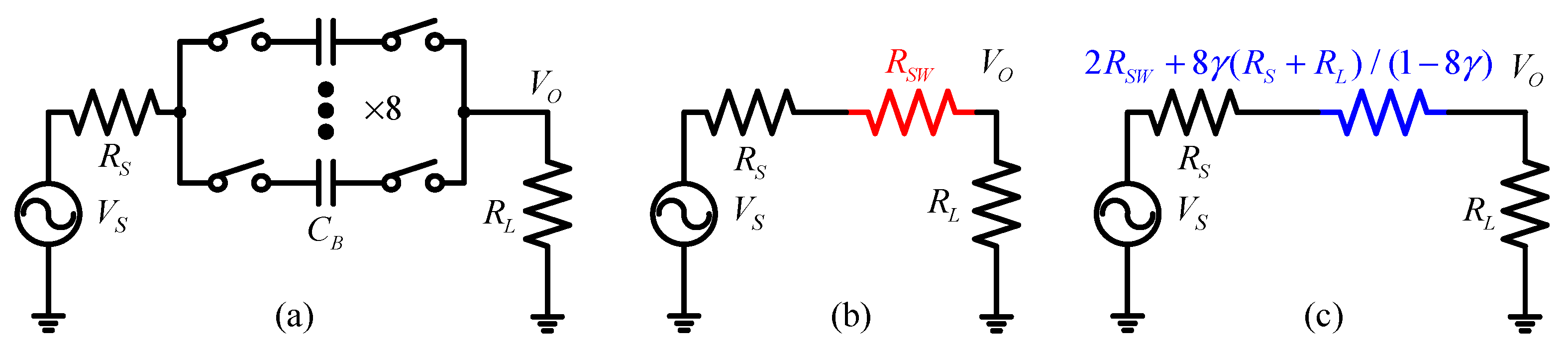
2. Basic Design of N-Path Notch Filter

Figure 2a illustrates the fundamental operation of the N-path BRF, which consists of a high-pass filter connected in series with a switch. This configuration shifts the high-pass filtering characteristics to the local oscillator (LO) frequency, generating the desired notch response. The mechanism effectively extends the high-pass filter’s utility to the target frequency band defined by the LO. Figure 2b shows that the N-path bandpass filter (BPF) operates with clock signals driven by a non-overlapping eight-phase clock waveform featuring a 12.5% duty cycle. The switching elements are modeled as ideal switches with a small series resistance, RSW, representing the on-resistance. This design assumption simplifies the analysis and highlights the impact of switching behavior on the overall filter characteristics [13,14]. Figure 2b shows that the N-path BPF and its clock waveforms are driven by a non-overlapping clock with an eight-phase 12.5% duty cycle. The switch is considered an ideal switch with a small series resistance RSW, which is the on-resistance.
The input impedance of the system is defined as RS. When a signal is applied, it passes through the series combination of the source resistance RS and the switch on-resistance RSW, with only one branch conducting at a time. Subsequently, the signal is connected in parallel with the eight ideal switches, as illustrated in Figure 3. Based on the derivation in other papers [15,16], the impedance equation for the N-channel band-stop filter can be obtained as:
Z i n = 2 R S W + R L + 2 R S W + R L + R a 8 γ 1 8 γ / / γ Z B B ω ω 0
where RL is the load impedance, and ZBB (ωω0) is the frequency-dependent baseband impedance.
The conventional N-path BRF exhibits a large impedance at the center frequency of the notch, corresponding to low block linearity, while presenting matched impedance characteristics within the passband, as illustrated in Figure 4. Under identical input power conditions, the large impedance state at the center frequency produces a significant voltage amplitude across the signal. This elevated voltage amplitude is directly applied across the source and drain terminals of the N-path filter’s switch. Consequently, this affects the Vgs of the MOS switch during both its on and off states, inducing nonlinearities in the filter’s operation.

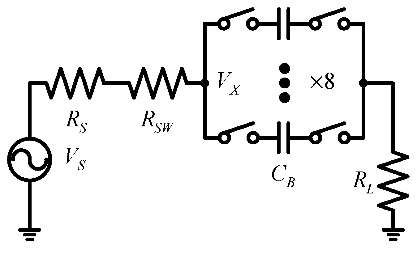
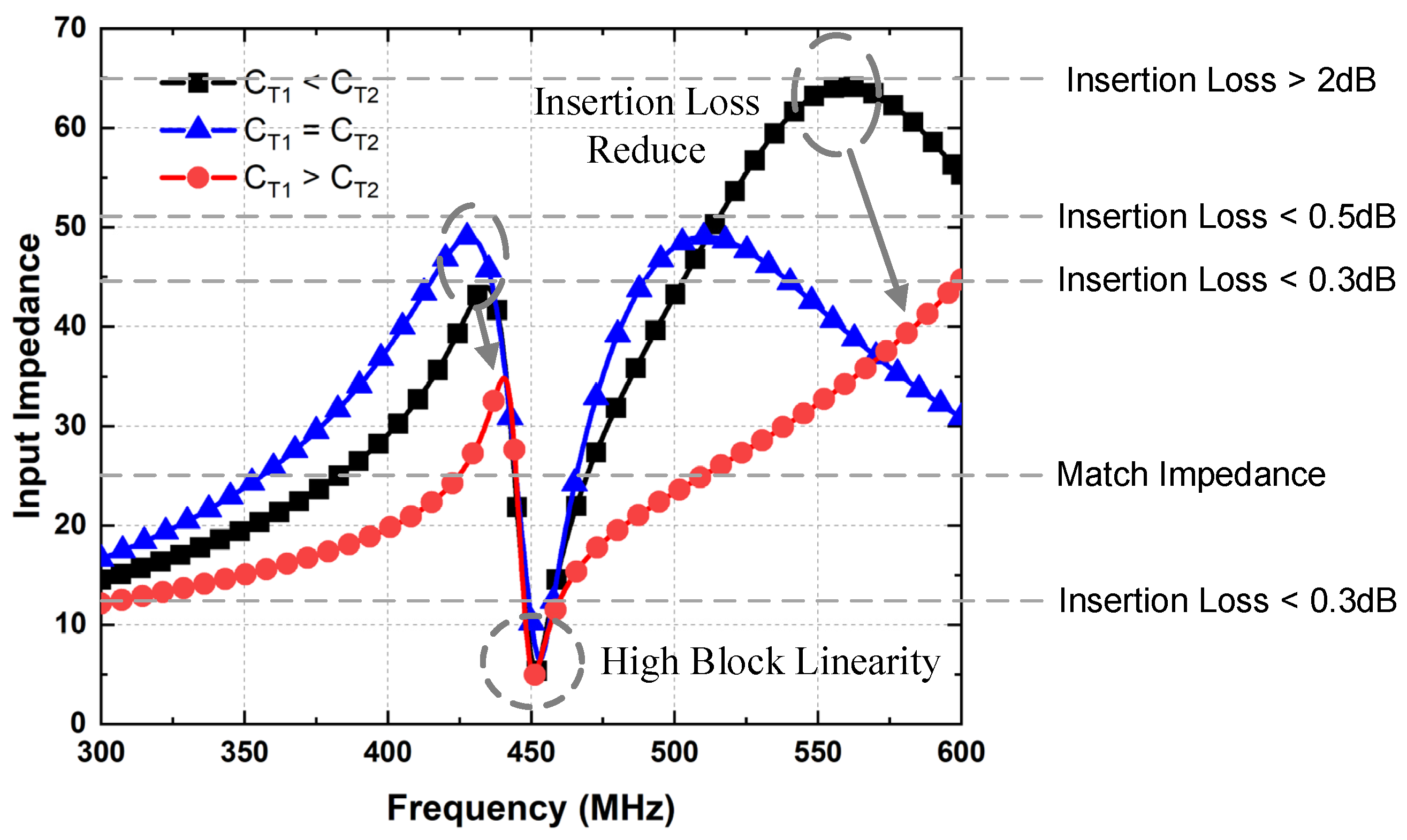
3. Proposed N-Path Notch Filter Architecture

The circuit diagram of the proposed N-path BRF is presented in Figure 5. At any given moment, one of the eight paths is active, with the high level of the clock signal enabling the corresponding MOS switch, while the other paths remain inactive. The high-linearity notch filter is designed with a two-stage cascade structure. Stage I comprises an N-path BPF with quarter-wavelength impedance transformation, enabling the notch filter functionality. This stage establishes a low-resistance path to the ground within the blocking band, thereby enhancing linearity. Stage II utilizes a conventional N-path BRF to further increase the overall rejection depth of the system. The switches of the N-path filter are driven by an eight-phase clock signal with a 12.5% duty cycle, ensuring precise timing and operation of the filter stages.
As illustrated in Figure 6, for SOI CMOS processes, the linearity of the N-path filter is constrained by the linearity of the MOS switches, which are designed to remain correctly on or off under clock control without accounting for switch-induced nonlinear distortion. With a 130 nm SOI CMOS process, the absolute value of Vgs must not exceed 2.5 V. For switches in the on state, the gate is subjected to a maximum voltage of VDD + VB, where a suitable DC bias VB is applied to the source and drain of the switch. The maximum positive swing of the input signal occurs when the on-state switch is critically closed and is given by:
V i n , p o s = V + V B = V D D V B V T H ,
where VTH is the threshold voltage of the MOS switch.
Similarly, the maximum negative swing of the input signal occurs when the off-state switch is critically open and is given by:
V i n , n e g = V B V = V B V E E + V T H
where VEE represents the voltage when the clock output is ‘0’, typically set to VEE = 0. VEE can be set to a negative voltage to improve linearity, as is further discussed in the subsequent sections. To ensure symmetrical voltage swings, the positive and negative swings should be equal, i.e., Vin,pos = Vin,neg. This condition leads to the equation:
V B = V D D + V E E 2 V T H 2
Thus, the maximum swing is as follows:
V + V B = V D D V E E 2
the maximum blocking power of the circuit, without inducing significant nonlinearity, can be calculated as:
P i n , m a x = 10 log [ V D D / 2 2 R e q u 2 ]
Requ is the impedance of the filter input port at the blocking frequency.
An excessive input amplitude during the positive voltage half-cycle results in a variation in the switch-on impedance, thereby inducing nonlinear distortion in the switch when it is in the on state. The resistance of the switch exhibits a dependence on the input signal amplitude, as expressed in Equation (7) [17]. Conversely, during the negative voltage half-cycle, an excessively large input amplitude causes the switch-off impedance to decrease or, in some cases, leads to unintended switching behavior, where the switch erroneously turns on despite being in the off state. This phenomenon generates nonlinear distortion, which is primarily due to charge sharing between different paths.
R S W = 1 μ C W L V D D V i n V T H )
According to Equation (6), the maximum Pin,max is obtained, with the ideal impedance characteristics of the band-stop filter, including low impedance in the stopband and matched impedance in the passband; this is achieved by the impedance transformation of the quarter-wavelength transmission line. As with the impedance characteristics of the N-path BRF, the input impedance Zin,sh of the N-path BPF is given by Equation (8). Stage I of the filter exhibits a matched impedance within the passband and a low impedance within the stopband, for a single-ended eight-path bandpass filter γ = 8 π 2 sin 2 π 8 0.1187 .
Z i n , s h ω = R S W + R S W + R S 8 γ 1 8 γ / / γ Z B B ω ω 0
The N-path BPF undergoes impedance transformation via a quarter-wavelength transmission line with an appropriately selected impedance, resulting in an impedance flip [18]. This transformation converts the input impedance from a matched impedance to a low impedance at the center frequency and from low impedance to a matched impedance as the frequency deviates from the center, as described in Equation (9):
Z i n , s h ω ~ = Z 0 2 R S W + R S W + R S 8 γ 1 8 γ / / γ Z B B ω ω 0
The transformed input impedance Equation (9) is substituted into Equation (6), obtaining a notch filter with high blocking power.
Quarter-wavelength transmission lines are characterized by specific frequencies and impedance values. In the RF range of this design, the size of the on-chip quarter-wavelength transmission line is too large to be implemented, and it can be equated by the structure of CLC, as shown in Figure 7a, and the structure of LCL, as shown in Figure 7b.
The CLC structure equivalent to a quarter-wavelength transmission line used the least amount of inductor. The CLC structure quarter-wavelength transmission lines’ specific frequencies were set to f = 450 MHz, and the transmission lines’ specific impedances were set to Zline = 25 Ω. The inductance and capacitance parameters in their CLC equivalent structure are calculated by Equations (10) and (11), L = 8.84 nH, C = 14.15 pF.
L = Z l i n e 2 π f
C = 1 2 π f Z l i n e
At this point the impedance characteristics of the notch filter can be rewritten as Equation (12), where QL is the Q value of the inductor in the CLC structure.
Z i n , s h ω = [ R S W + R S W + R S 8 γ 1 8 γ γ Z B B ω ω 0 1 j ω C T 1 + j ω L + ω L Q L ] 1 j ω C T 2
The quality factor of the inductor affects the impedance characteristics of the filter after it has been transformed by the CLC structure. First, for the reject band impedance, the baseband capacitor impedance Z B B ω ω 0 is approximately equal to the load impedance ZB, and the reject impedance can be expressed as Equation (14). Next, the analyzed passband impedance can be expressed as Equation (15). From here, the resistance introduced by the finite inductor Q factor can actually be corrected by an increase in CT1 or a decrease in CT2. Therefore, the quality factor does not limit the impedance of the filter’s reject band or the linearity. However, this adjustment leads to a shift in the transmission line’s characteristic frequency toward higher frequency.
Z B R S
Z i n , r e j e c t ω = R S W + R S W + R S 8 γ 1 8 γ γ Z B 1 j ω C T 1 + j ω L + ω L Q L 1 j ω C T 2
Z i n , p a s s ω R S W 1 j ω C T 1 + j ω L + ω L Q L 1 j ω C T 2
The simulation of the CLC uses an ideal inductor versus finite quality factor inductor equivalent structure with an ideal quarter-wavelength transmission line; the adjusted CLC structure is shown in Figure 8a, where it can be concluded that the CLC structure is approximately equivalent to a quarter-wavelength transmission line in 0 to 600 MHz, and equivalent deterioration of the impedance transformation at the band edges leads to an additional differential loss shortfall and poor equivalence at high frequencies due to its low-pass filtering characteristics. The adjusted CLC structure can correct the equivalent situation of the CLC structure, sacrifice low-frequency differential loss, and reduce high-frequency insertion loss substantially by affecting the capacitance on the low-impedance side, making an adjustable balance between low-frequency and high-frequency insertion loss. At the same time, the quality factor of the inductor affects the transmission line loss, which is reflected in the additional insertion loss of the filter, as shown in Figure 8b; as the Q value of the inductor decreases, the overall differential loss of the filter increases, and the characteristic frequency of the transmission line moves to lower frequency, resulting in asymmetry of the insertion loss on both sides of the operated frequency band, which requires a continued increase in CT1 and decrease in CT2. The off-chip inductor with the appropriate quality factor is selected in forming a balance between size and differential loss. In this design, the value of the inductor Q factor is chosen to be 80.
In this design, the RF range of 300 to 600 MHz, the transmission line’s bandwidth influences the impedance conversion’s effectiveness, particularly at the band’s edges, where the conversion becomes less efficient. As the bandwidth increases, the insertion loss shortfall also becomes more significant. This impedance mismatch results in an increased insertion loss of the filter. To mitigate this issue, an adjustable transmission line structure can be employed to compensate for the resulting shortfall in insertion loss. As shown in Figure 9, without modulating the transmission line structure, for the CT1 = CT2 curve in the figure, the parasitic capacitance on the Stage II side is larger due to the parasitic factor, resulting in the CT1 < CT2 curve in the corresponding figure; in this case, the insert shortfall at the edge of the filter band grows greater than 2 dB, and the filter loss increases. By adjusting the equivalent structure of the transmission line, it is possible to achieve the CT1 > CT2 curve in the figure, where the insert shortfall at the edge of the filter band grows less than 0.3 dB. The proposed filter utilizes a matching impedance of 25 Ω, which minimizes insertion loss at the lower transmission line impedances and increases insertion loss at the higher impedances. The overall insertion loss is influenced by parasitic capacitances inherent to the chip and the bandwidth of the transmission line. By appropriately adjusting the values of CT1 and CT2, the insertion loss is effectively reduced.

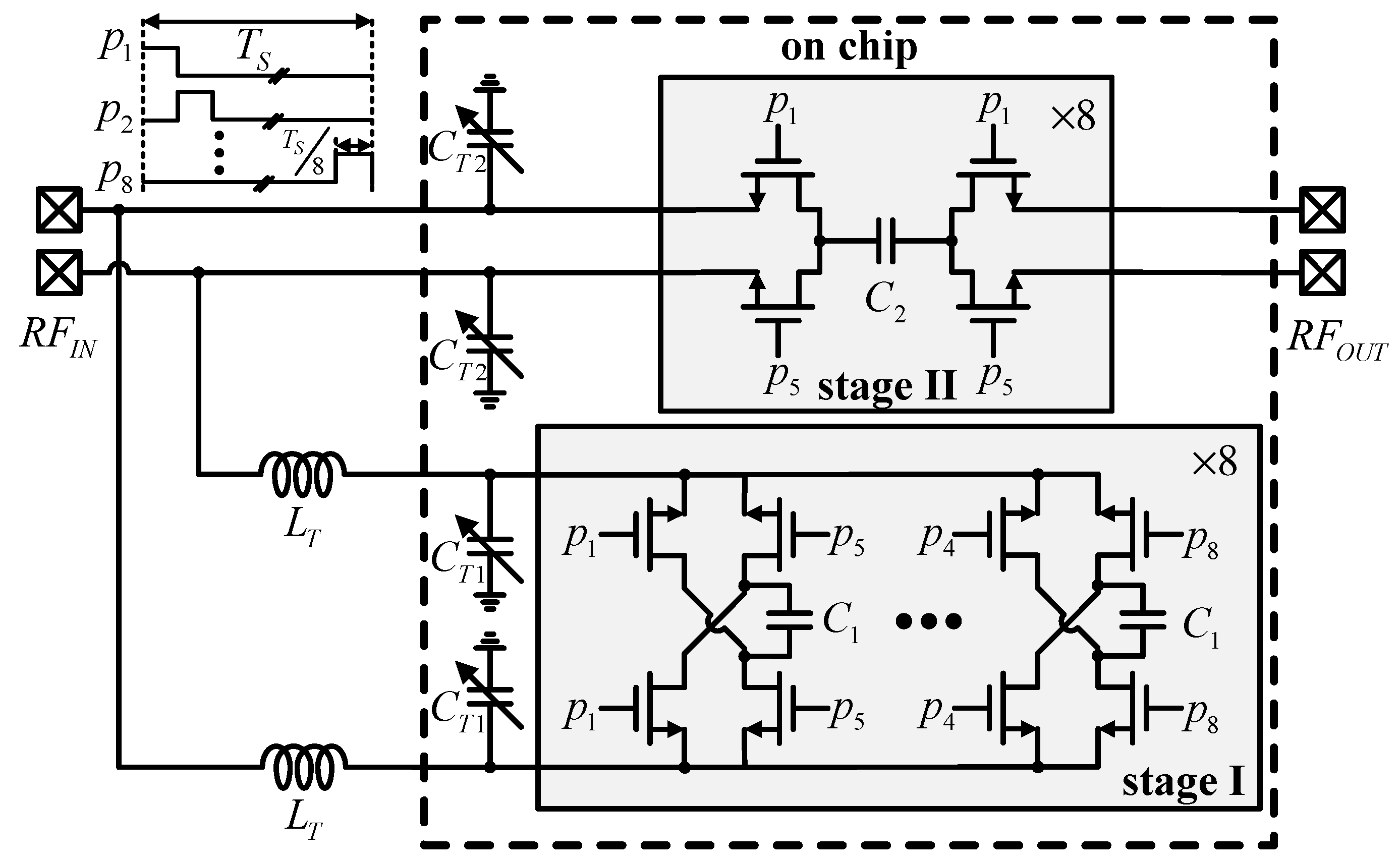
4. Circuit Implementation

The schematic for the proposed filter is depicted in Figure 5. It features an eight-path notch filter with an in-band impedance flip-flop, driven by an eight-phase 12.5% duty cycle clock to achieve high linearity in blocker power rejection. High blocker power suppression is facilitated by a quarter-wavelength transmission line, which, combined with an N-path BPF in Stage I and an N-path BRF in Stage II, ensures a high rejection depth. Off-chip LC equivalents are utilized for the quarter-wavelength transmission lines to minimize chip area. The filter architecture includes an eight-path N-path BPF, an eight-path N-path BRF, two off-chip LC equivalent models, and an eight-phase 12.5% duty cycle clock generator.

4.1. N-Path Filter Architecture of Stage I and Stage II

A detailed schematic is presented in Figure 5. Within the BPF, off-chip quarter-wavelength transmission line transformation is employed, with the resultant impedance affecting both the blocking power and the depth of band rejection. All filter capacitance is realized using MIM capacitors. The N-path BPF and BRF switches utilize NMOS transistors with a low threshold voltage and a 2.5 V drain and source breakdown voltage to achieve high linearity. The rejection depth is enhanced by minimizing parasitic resistance in the switch and capacitor RF lines [18]. After conversion, the impedance in the blocking band is reduced to improve blocking linearity. Parasitic resistance in the switches also impacts the filter’s insertion loss. The N-path filter’s switch size W/L is equal to 240 µm/220 nm and achieves an on-resistance of approximately 4 Ω, which reduces passband insertion loss and enhances notch rejection. The NMOS drain and source are biased with a 0.5 V voltage to optimize linearity.

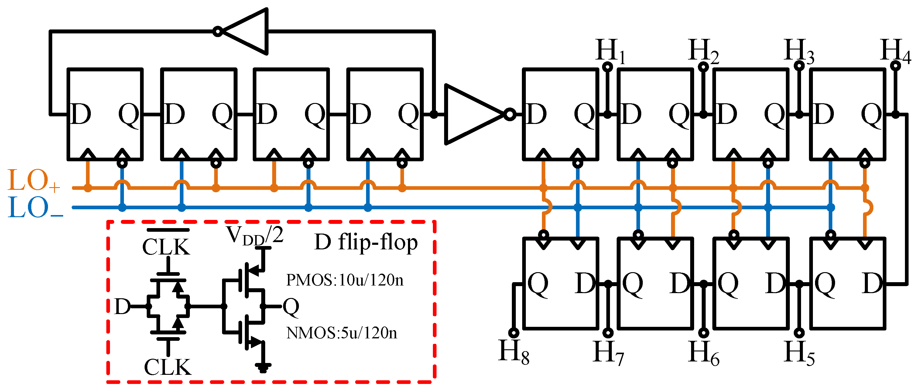
4.2. Eight-Phase 12.5% Duty Cycle Clock Generator

The eight-phase 12.5% duty cycle clock generator schematic is shown in Figure 10. A single-ended sinusoidal clock input clock balun with 4× fLO inputs is used to generate a symmetrical differential clock, LO+ and LO−. The clock balun is realized by a same-size inverter with a transmission gate that compensates for delays to minimize differential signal phase errors. The divide-by-four ring counter circuit, composed of D flip-flops, generates eight phase-shifted signals, each with a 50% duty cycle and a 12.5% phase shift between successive paths. The eight-phase, 12.5% duty cycle clock is derived from eight NAND gates [19]. Preceding the eight-phase clock, a duty cycle calibration module and a buffer circuit ensure accurate signal generation. The large filter switch size leads to larger output buffer size and increased clock dynamic power consumption.

4.2.1. Divider

The divide-by-four ring counter uses a D flip-flop, as shown in Figure 11. The divide-by-four on the input signal 4× fLO quadrature generates a frequency of fLO and a 50% duty cycle signal; after eight D flip-flops, it generates an eight-phase 45° phase-shifted, 50% duty cycle from the intermediate signal. The D flip-flop consists of a differential clock-controlled transmission gate in series with an inverter to achieve the highest inversion speeds, in which the size of NMOS is 5 µm/120 nm, and the size of PMOS is 10 µm/120 nm. The eight-phase signal becomes eight NAND to generate an eight-phase, 45° phase-shifted, 12.5% duty cycle from the clock signals. Normally, adding an intermediate dummy d flip-flop is necessary to balance the phase error; clock phase differences affect the differential loss of filters.

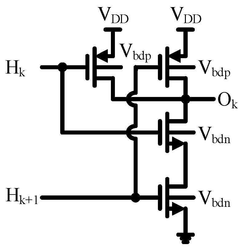
4.2.2. NAND and Duty Cycle Calibration

The NAND circuit is shown in Figure 12. In the NAND combination of two sets of crossed inverters, the size of NMOS is 5 µm/120 nm and the size of PMOS is 10 µm/120 nm. Controlling the body voltage Vbdn of NMOS and Vbdp of PMOS in NAND adjusts the duty cycle of the output clock. The ideal clock duty cycle for an eight-path filter is 12.5%. A duty cycle that is too large can lead to filter aliasing; a duty cycle that is too small can lead to increased filter loss. The clock duty cycle is also adjusted by adjusting the bias voltage at the body end of the NMOS and PMOS in the duty cycle calibration circuit.

4.3. Off-Chip LC Equivalent Model

In the frequency range of 300 to 600 MHz, the RF signal wavelength varies from approximately 1 m to 0.5 m. As a result, the size of the quarter-wavelength transmission line becomes impractically large, contributing significantly to both the design cost and chip area. To address this challenge, the simplest approach involves using off-chip lumped LC equivalents. For this purpose, a CLC network incorporating a single inductor is employed. Specifically, considering the inductive effect of bonding wires, an 8 nH wire-wound ceramic chip inductor with a Q factor of 80 is chosen to minimize passband loss. The inductance value is adjusted to modulate the transmission line’s eigenfrequency, while the capacitances CT1 and CT2 in the CLC network are controlled on-chip through multiplier capacitor arrays. To achieve the desired filter performance, these capacitors have values ranging from 1 to 63 pF, adjustable in 1 pF steps.

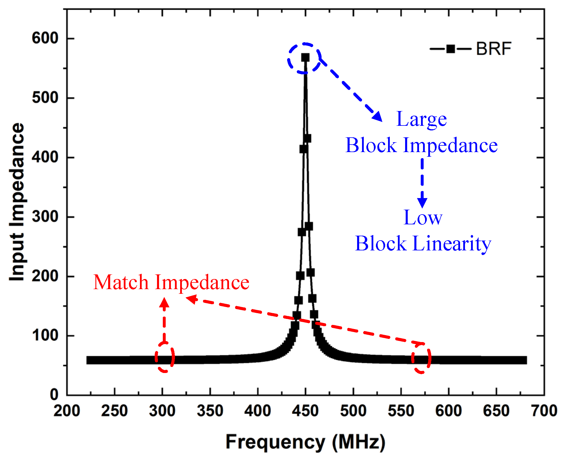
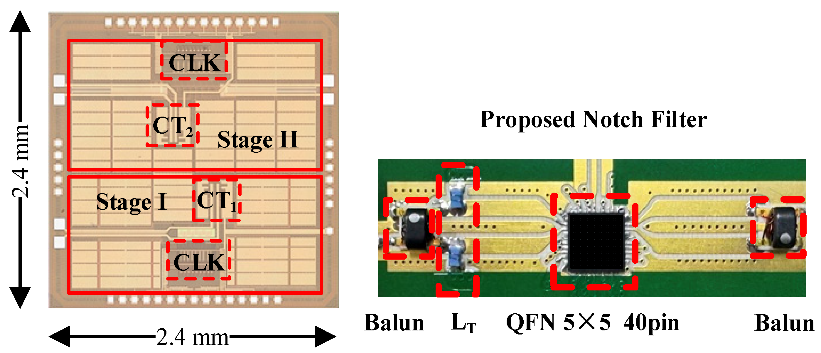
5. Measurement Results
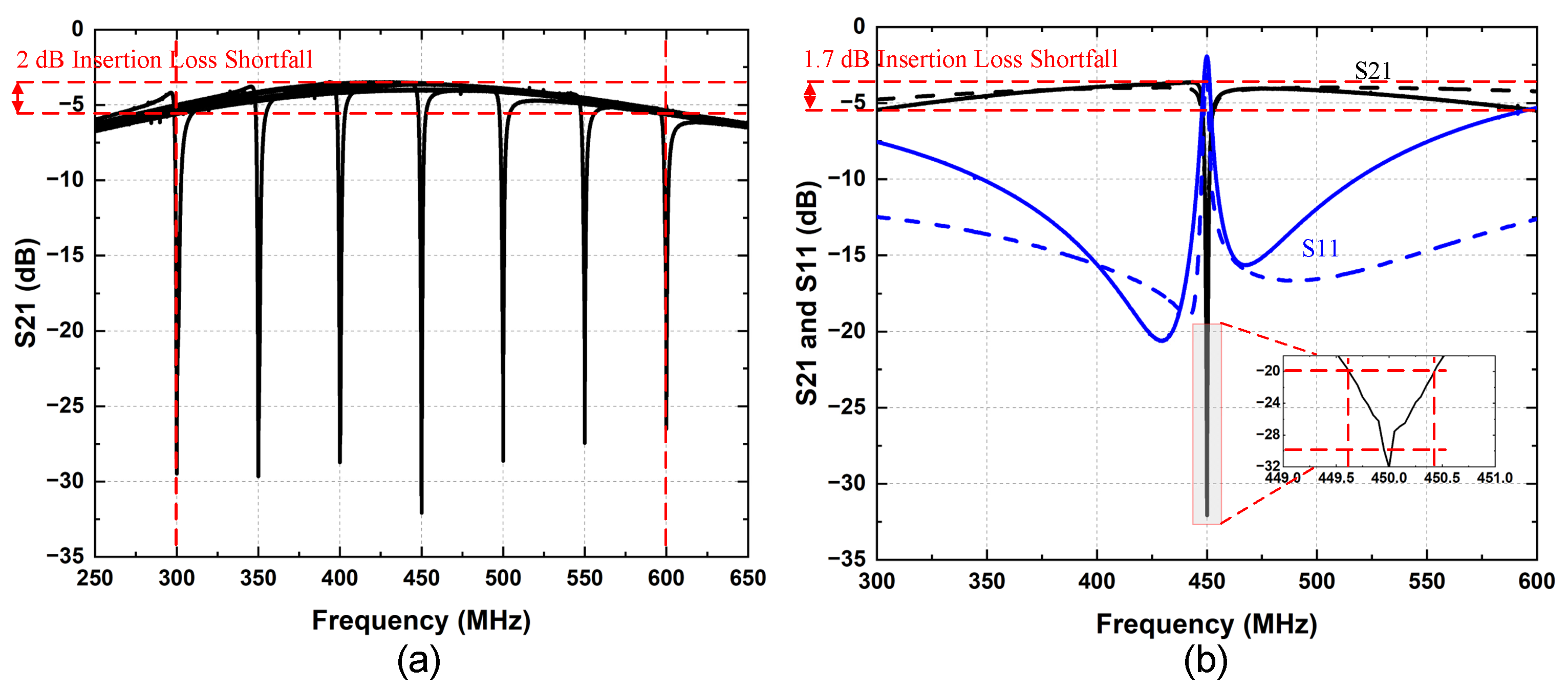
A high-linearity N-path notch filter is implemented using a 130 nm RFSOI process, and the die micrograph is depicted in Figure 13. The total chip area is 2.4 × 2.4 mm2, with the active filter area occupying 0.25 mm2. To achieve the differential structure, two off-chip 1:1 balun (mini-circuits TC1-1-13MG2+) are used at the RF input and output ports. The chip is mounted in a QFN 40 package and tested on a PCB. Losses due to cables and PCB signal traces are de-embedded during measurement to ensure accurate results. The power consumption is measured to range from 186 to 242 mW within the 300 to 600 MHz RF range under a 12 dBm high TX blocker. The primary power consumption is attributed to the buffer, which drives large switches with an eight-phase nonoverlap 12.5% duty cycle clock.

5.1. S-Parameters

The measured S21 of the proposed notch filter across the RF tuning range is shown in Figure 14a. To minimize the loss of receiver channel bandwidth, the 3 dB passband bandwidth of the proposed notch filter ranges from 3.5 to 4 MHz across the RF tuning range. The details of the measured and simulation results at fLO = 450 MHz are provided in Figure 14b. For a QAM64 signal with a baseband bandwidth of 800 kHz, the filters achieve a rejection greater than 20 dB over the entire frequency range and zoom in through the details, with a maximum rejection exceeding 25 dB.
The frequency corresponding to the quarter-wavelength transmission line characteristic impedance is about 450 MHz to equalize the performance over the entire frequency band. The passband differential loss at the edge of the band increases by 2 dB due to the variation in the transmission line wavelength, which a more complex LC structure can reduce. However, it also requires the use of more off-chip inductance. The insertion loss shortfall reduces from 3.8 dB to 2 dB across 300 MHz to 600 MHz via adjustable CT1 and CT2. The filter insertion loss is 3.6 to 5.4 dB at fLO= 450 MHz with a 1.8 dB insertion loss shortfall. This insertion loss is acceptable for multiple SAW filters in a switched array configuration, as shown in Figure 14b.

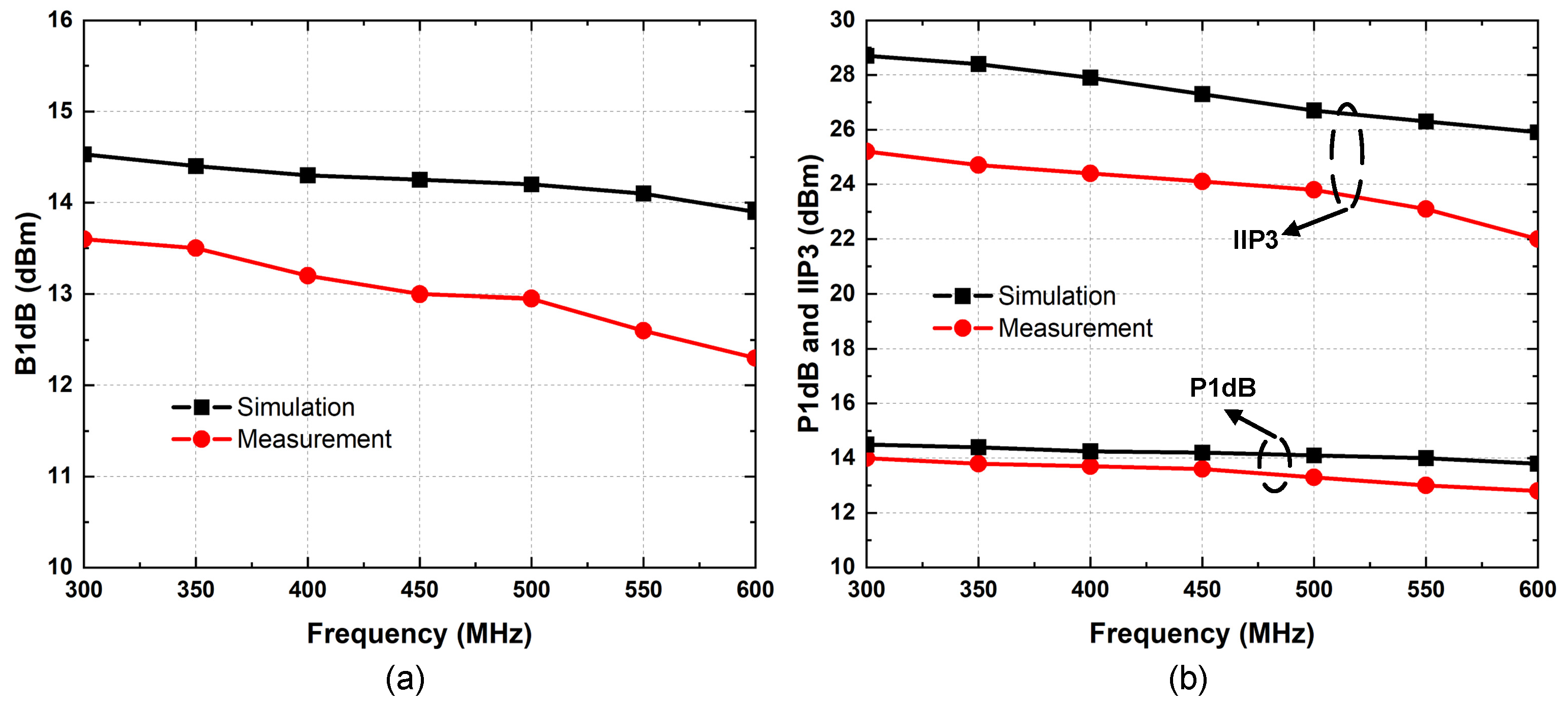
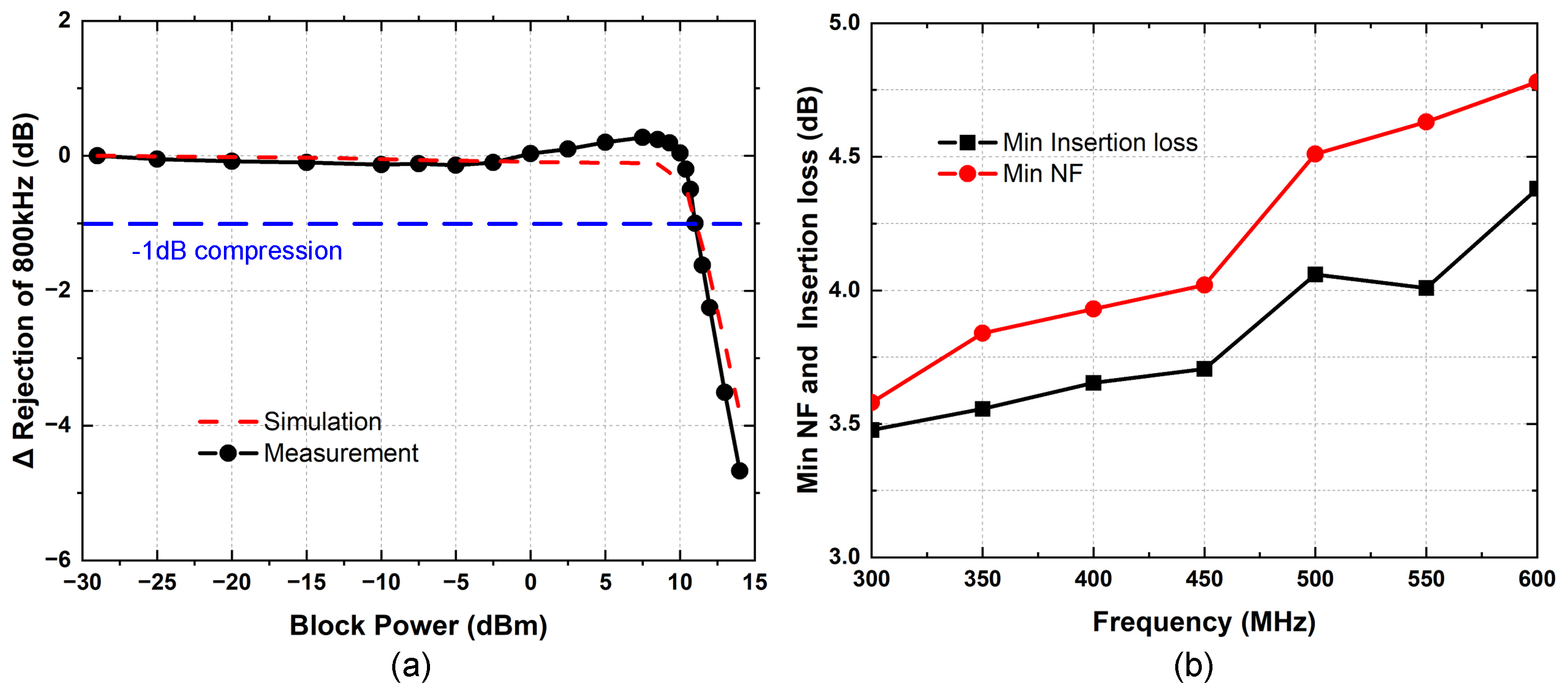
5.2. Linearity and NF

A single tone at fLO is used to measure B1dB. A single tone at fLO + 20 MHz is used to measure P1dB in the passband. The third-order input-intercept-point (IIP3) profile is measured by injecting two-tone tests with a frequency at fLO + 20 MHz and fLO + 21 MHz. The large block signal causes compression of the desired signal. The measured blocker B1dB is 12.3 to 13.6 dBm. The measured P1dB is 12.8 to 14 dB, and the IIP3 ranges between 22.3 and 25.2 dBm across the tuning range, as shown in Figure 15.
Figure 16a shows rejection for a bandwidth of 800 khz versus block power at fLO = 450 MHz. The notch depth was degraded by 1 dB for a 12 dBm block power, and the filter maintained >20 dB of rejection for a bandwidth of 800 kHz. In the RF tuning range, the min NF is 3.58 dB to 4.78 dB, as shown in Figure 16b. The NF at 600 MHz goes up by 1.2 dB. The blocker noise figure (BNF) is measured in the presence of a TX signal located at fLO = 450 MHz and is plotted in Figure 17. The NF increases to around 9 dB with a 12 dBm TX leakage.
Table 1 summarizes the power consumption at different frequencies when the proposed notch filter is tuned from 0.3 to 0.6 GHz. With a 12 dBm TX leakage, the clock power consumption is 186 to 242 mW over the tuning range. Table 1 shows that the switch buffers mainly consume power, which drives the large switches with eight-phase nonoverlap 12.5% duty cycle clocks. The buffer power consumption is proportional to the switch size, with smaller switch sizes leading to lower insertion loss.
Table 2 summarizes the performance of the proposed notch filter and compares the measured results with state-of-the-art N-path-based passive notch filters. The filter linearity and maximum rejection are substantially improved compared to the conventional LNA shunt notch structure [19]. Compared to the N-path bandpass filter with a series notch architecture presented in [12], the proposed filter demonstrates advantages in both B1dB and P1dB, while also meeting the requirements of wideband receivers and reducing power consumption simultaneously. Compared with [20,21], the proposed filter exhibits improved B1dB and P1dB. It is comparable to that in [22] in terms of noise and rejection performance, but with a large improvement in passband IIP3. Furthermore, compared to the design in [16], which utilizes an N-path inverted shunt notch architecture, the proposed filter incorporates an adjustable transmission line structure. This design effectively reduces insertion loss by optimizing impedance and achieves a smaller insertion loss shortfall across the RF tuning range.

6. Conclusions

This paper presents a blocker N-path notch filter for TX leakage suppression in a wideband receiver. The transmission line achieves an impedance flip within the block band to improve the linearity of blocker suppression. The adjustable CLC transmission line minimizes insertion loss shortfall in the tuning range. The filter achieves >25 dB rejection for a 12.3 to 13.6 dBm TX leakage blocker and 12.8 to 14 dBm P1dB. At the same time, the passband IIP3 of up to 22 to 25.2 dBm is realized, maximizing the dynamic range of the receiving channel. The design of the adjustable transmission line structure is analyzed to reduce the insertion loss in terms of impedance and to achieve 1.7 to 2 dB insertion loss shortfall over 300 to 600 MHz. Due to its high linearity, the TX leakage can be effectively filtered out in the front end of a broadband receiver, improving the receiver sensitivity.

Author Contributions

Conceptualization, X.L.; methodology, X.L. and S.Q.; software, X.L. and S.X.; validation, X.L., S.Q. and S.X.; formal analysis, X.L.; investigation, X.L.; resources, Q.X., G.W. and L.Z.; data curation, X.L. and H.Z.; writing—original draft preparation, X.L.; writing—review and editing, X.L.; visualization, X.L.; supervision, G.W. and L.Z.; project administration, L.Z.; funding acquisition, G.W. and L.Z. All authors have read and agreed to the published version of the manuscript.

Funding

This research received no external funding.

Data Availability Statement

The datasets produced and/or analyzed in the present study are available from the corresponding author upon reasonable request.

Conflicts of Interest

The authors assert that they do not have any conflicts of interest.

Abbreviations

The following abbreviations are used in this manuscript:
TXTransmitter
RXReceiver
B1dBBlocker 1 dB compression point
P1dB1 dB compression point
IIP3Third-order input intercept point
SAWSurface acoustic wave
BAWBulk acoustic wave
SCSwitched capacitor
BRFBand reject filters
BPFBandpass filter
LOLocal oscillator
VgsGate-to-source voltage
PCBPrinted circuit board
NFNoise figure
BNFBlocker noise figure

References

  1. Gao, C.; Zheng, Y.; Li, H.; Ren, Y.; Gu, X.; Huang, X.; Wang, Y.; Qu, Y.; Liu, Y.; Cai, Y.; et al. Design and Fabrication of a Film Bulk Acoustic Wave Filter for 3.0 GHz–3.2 GHz S-Band. Sensors 2024, 24, 2939. [Google Scholar] [CrossRef] [PubMed]
  2. Li, G.; Xu, W.; Nan, J.; Gao, M. Design of Efficient Concurrent Dual-Frequency Doherty Power Amplifier Based on Step Impedance Low-Pass Filter. Electronics 2023, 12, 4092. [Google Scholar] [CrossRef]
  3. Lin, Y.-S.; Huang, C.-Y.; Huang, C.-T.; Chang, J.-F.; Tien, N.-W.; Chuang, Y.-H. Design and Analysis of Complementary Metal–Oxide–Semiconductor Single-Pole Double-Throw Switches for 28 GHz 5G New Radio. Electronics 2023, 12, 4156. [Google Scholar] [CrossRef]
  4. Chen, R.; Sheng, Q.; Zhou, L.; Chen, C.; Zhang, H. High-Q Bandpass-to-Bandstop Reconfigurable Filter Based on SAW Resonators. In Proceedings of the 2020 IEEE/MTT-S International Microwave Symposium (IMS), Los Angeles, CA, USA, 4–6 August 2020; pp. 123–126. [Google Scholar]
  5. Darabi, H. A Blocker Filtering Technique for SAW-Less Wireless Receivers. IEEE J. Solid-State Circuits 2007, 42, 2766–2773. [Google Scholar] [CrossRef]
  6. Safarian, A.; Shameli, A.; Rofougaran, A.; Rofougaran, M.; de Flaviis, F. Integrated Blocker Filtering RF Front Ends. In Proceedings of the 2007 IEEE Radio Frequency Integrated Circuits (RFIC) Symposium, Honolulu, HI, USA, 3–5 June 2007; pp. 13–16. [Google Scholar]
  7. Ghaffari, A.; Klumperink, E.A.M.; Nauta, B. Tunable N-Path Notch Filters for Blocker Suppression: Modeling and Verification. IEEE J. Solid-State Circuits 2013, 48, 1370–1382. [Google Scholar] [CrossRef]
  8. Lin, Z.; Mak, P.-I.; Martins, R.P. Analysis and Modeling of a Gain-Boosted N-Path Switched-Capacitor Bandpass Filter. IEEE Trans. Circuits Syst. I Regul. Pap. 2014, 61, 2560–2568. [Google Scholar] [CrossRef]
  9. Qi, G.; Mak, P.-I. A 0.5-to-1.5 GHz BW-Extended Gain-Boosted N-Path Filter Using a Switched gm−C Network Achieving 50 MHz BW and 18.2dBm OB-IIP3. In Proceedings of the 2023 IEEE Asian Solid-State Circuits Conference (A-SSCC), Haikou, China, 5–8 November 2023; pp. 1–3. [Google Scholar]
  10. Klumperink, E.A.M.; Westerveld, H.J.; Nauta, B. N-path filters and mixer-first receivers: A review. In Proceedings of the 2017 IEEE Custom Integrated Circuits Conference (CICC), Austin, TX, USA, 30 April–3 May 2017; pp. 1–8. [Google Scholar]
  11. Haq, T.; Koziel, S.; Pietrenko-Dabrowska, A. Resonator-Loaded Waveguide Notch Filters with Broad Tuning Range and Additive-Manufacturing-Based Operating Frequency Adjustment Procedure. Electronics 2023, 12, 4486. [Google Scholar] [CrossRef]
  12. Luo, C.-K.; Gudem, P.S.; Buckwalter, J.F. A 0.2–3.6-GHz 10-dBm B1dB 29-dBm IIP3 Tunable Filter for Transmit Leakage Suppression in SAW-Less 3G/4G FDD Receivers. IEEE Trans. Microw. Theory Tech. 2015, 63, 3514–3524. [Google Scholar] [CrossRef]
  13. Dougherty, C.M.; Xue, L.; Pulskamp, J.; Bedair, S.; Polcawich, R.; Morgan, B. A 10 V Fully-Integrated Switched-Mode Step-up Piezo Drive Stage in 0.13 um CMOS Using Nested-Bootstrapped Switch Cells. IEEE J. Solid-State Circuits 2016, 51, 1475–1486. [Google Scholar] [CrossRef]
  14. Hasan, M.N.; Saeedi, S.; Gu, Q.J.; Sigmarsson, H.H.; Liu, X. Design Methodology of N-Path Filters with Adjustable Frequency, Bandwidth, and Filter Shape. IEEE Trans. Microw. Theory Tech. 2018, 66, 2775–2790. [Google Scholar] [CrossRef]
  15. Qi, G.; Mak, P.-I.; Martins, R.P. A 0.038-mm2 SAW-Less Multiband Transceiver Using an N-Path SC Gain Loop. IEEE J. Solid-State Circuits 2017, 52, 2055–2070. [Google Scholar] [CrossRef]
  16. Andrews, C.; Molnar, A.C. Implications of Passive Mixer Transparency for Impedance Matching and Noise Figure in Passive Mixer-First Receivers. IEEE Trans. Circuits Syst. I Regul. Pap. 2010, 57, 3092–3103. [Google Scholar] [CrossRef]
  17. Reiskarimian, N.; Krishnaswamy, H. Design of all-passive higher-order CMOS N-path filters. In Proceedings of the 2015 IEEE Radio Frequency Integrated Circuits Symposium (RFIC), Phoenix, AZ, USA, 17–19 May 2015; pp. 83–86. [Google Scholar]
  18. AlShammary, H.; Hill, C.; Hamza, A.; Buckwalter, J.F. A λ/4-lnverted N-path Filter in 45-nm CMOS SOI for Transmit Rejection with Code Selective Filters. In Proceedings of the 2018 IEEE/MTT-S International Microwave Symposium—IMS, Philadelphia, PA, USA, 10–15 June 2018; pp. 1370–1373. [Google Scholar]
  19. Pourbagheri, S.; Mayaram, K.; Fiez, T.S. A self-clocked blocker-filtering technique for SAW-less wireless applications. In Proceedings of the 2016 IEEE Radio Frequency Integrated Circuits Symposium (RFIC), San Francisco, CA, USA, 22–24 May 2016; pp. 250–253. [Google Scholar]
  20. Khorshidian, M.; Reiskarimian, N.; Krishnaswamy, H. 29.4 High-Performance Isolators and Notch Filters Based on N-Path Negative Transresistance. In Proceedings of the 2020 IEEE International Solid-State Circuits Conference—(ISSCC), San Francisco, CA, USA, 16–20 February 2020; pp. 446–448. [Google Scholar]
  21. Lee, D.; Yun, S.; Kwon, K. IIP2-Enhanced Receiver Front-End with Notch-Filtered Low-Noise Transconductance Amplifier for 5G New Radio Cellular Applications. In Proceedings of the 2023 IEEE Radio Frequency Integrated Circuits Symposium (RFIC), San Diego, CA, USA, 11–13 June 2023; pp. 25–28. [Google Scholar]
  22. Kim, H.; Jo, S.; Kwon, K. Channel-Selection LNA Using High-Order N-Path Feedforward Blocker Cancellation Path with Complex Poles for Advanced 5G NR FDD RX. IEEE Trans. Microw. Theory Tech. 2024, 72, 6821–6832. [Google Scholar] [CrossRef]
Figure 1. A large blocker causes saturation of the RX system and notch filter.
Electronics 14 00854 g001
Figure 2. (a) Operation of N-path BRF. (b) fin away from fLO. (c) fin equal to fLO.
Electronics 14 00854 g002
Figure 3. N-path filter with switched impedance equivalent modeling.
Electronics 14 00854 g003
Figure 4. N-path BRF impedance characteristic curve at fLO = 450 MHz.
Electronics 14 00854 g004
Figure 5. Schematic of the proposed N-path notch filter.
Electronics 14 00854 g005
Figure 6. (a) N-path BRF schematic, (b) filter switch bias voltage.
Electronics 14 00854 g006
Figure 7. (a) CLC equivalent structure; (b) LCL equivalent structure.
Electronics 14 00854 g007
Figure 8. (a) The CLC structure Q factor influences inductors and adjusts the CLC structure. (b) Effect of different Q factors of inductor.
Electronics 14 00854 g008
Figure 9. Inverted impedance curve of proposed notch filter at fLO = 450 MHz.
Electronics 14 00854 g009
Figure 10. The schematic of the clock generator.
Electronics 14 00854 g010
Figure 11. The divide-by-four ring counter circuit.
Electronics 14 00854 g011
Figure 12. The NAND circuit.
Electronics 14 00854 g012
Figure 13. Chip micrograph and assembled board of the notch filter with CLC inductor LT.
Electronics 14 00854 g013
Figure 14. (a) Measured S21 of the proposed notch filter across the RF tuning range; (b) measured S21 and S11 at fLO = 450 MHz. Some variations between measurements (solid) and simulations (dashed) were observed.
Electronics 14 00854 g014
Figure 15. (a) Measured and simulation B1dB across the RF tuning range; (b) measured and simulation P1dB and IIP3 across the RF tuning range.
Electronics 14 00854 g015
Figure 16. (a) Rejection versus block power at fLO = 450 MHz; (b) measured min NF across RF tuning range.
Electronics 14 00854 g016
Figure 17. Measured and simulated BNF with a blocker located at 450 MHz.
Electronics 14 00854 g017
Table 1. Power consumption table with 12 dBm TX leakage.
With 12 dBm TX LeakageFrequency = 0.3 GHzFrequency = 0.6 GHz
Clock Balun7.29.1
Divider5.18.5
NANDs and Duty Cycle Calibration26.528.6
Buffers147.2195.8
Total186242
Table 2. Performance summary and comparison.
Reference[19][20][21][22][12][16]This Work
Technology65 nm CMOS65 nm CMOS65 nm CMOS65 nm CMOS45 nm SOI45 nm SOI130 nm SOI
TopologyN-path
LNA
+ Shunt
Notch
N-path
Neg. Trans-Res. Notch
LNTA +
Dual-Band
LC Notch
CS-LNA BPF+
FF Blocker
Cancelling Notch
N-path
BPF
+ Series Notch
N-path
Inv. Shunt
Notch
N-path
Adjustable Inv. Shunt Notch
+ Series Notch
RF Range/GHz1 to 1.60.2 to 10.7 to 2.21.35 to 2.70.2 to 3.60.9 to 1.10.3 to 0.6
BW/MHzN/A28 (20 dB BW)N/A>48>8012 to 25 (3 dB BW)3.5 to 4 (3 dB BW)
0.8 (20 dB BW)
B1dB/dBm−10 #5 to 7−18 to −6 #>7.510 #N/A12.3 to 13.6
P1dB/dBmN/AN/A>−40N/A4 #>−1012.8 to 14
IB IIP3/dBmN/A17 to 21.5−14.54.8 to 5.82222.6 *22 to 25.2
Insertion Loss Shortfall/dB<1 #>4 #>3 #N/A2 #>3 #1.7 to 2
DSB NF/dB51 to 43.5 to 4.44.4 to 4.62.8 to 4.54 to 53.58 to 4.78
Max Rejection/dB19>50>25>23.8412327 to 32
Power Con./mW3017 to 21.511.721.2183.3 to 303.5 6.18186 to 242
* This chip works in N-Path mode. # Estimate from figure. With 9 dBm TX blocker.
Disclaimer/Publisher’s Note: The statements, opinions and data contained in all publications are solely those of the individual author(s) and contributor(s) and not of MDPI and/or the editor(s). MDPI and/or the editor(s) disclaim responsibility for any injury to people or property resulting from any ideas, methods, instructions or products referred to in the content.

