
A Compact and High-Efficiency Design of Triple-Band Rectifier for Wireless Power Transfer


Abstract
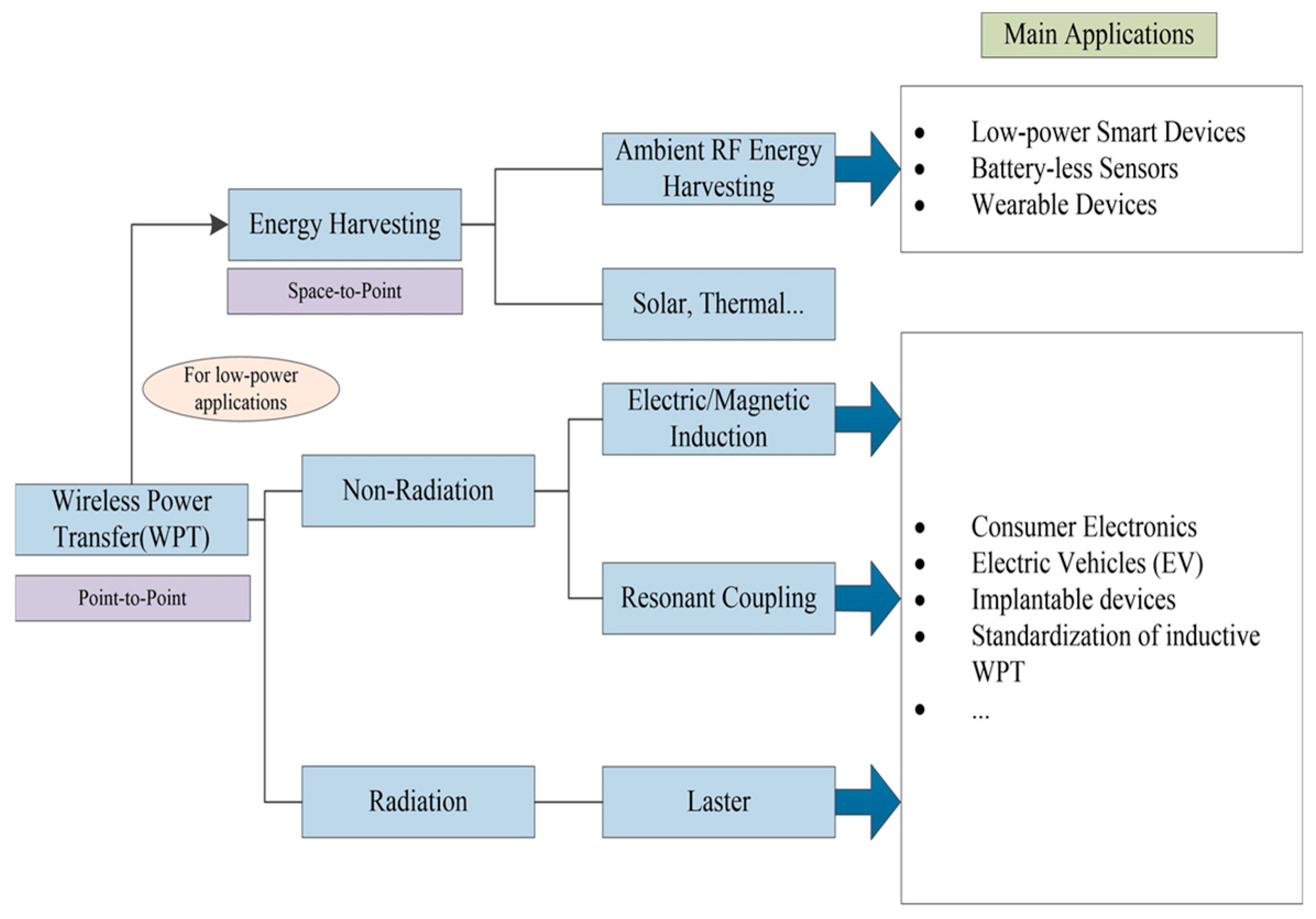
1. Introduction
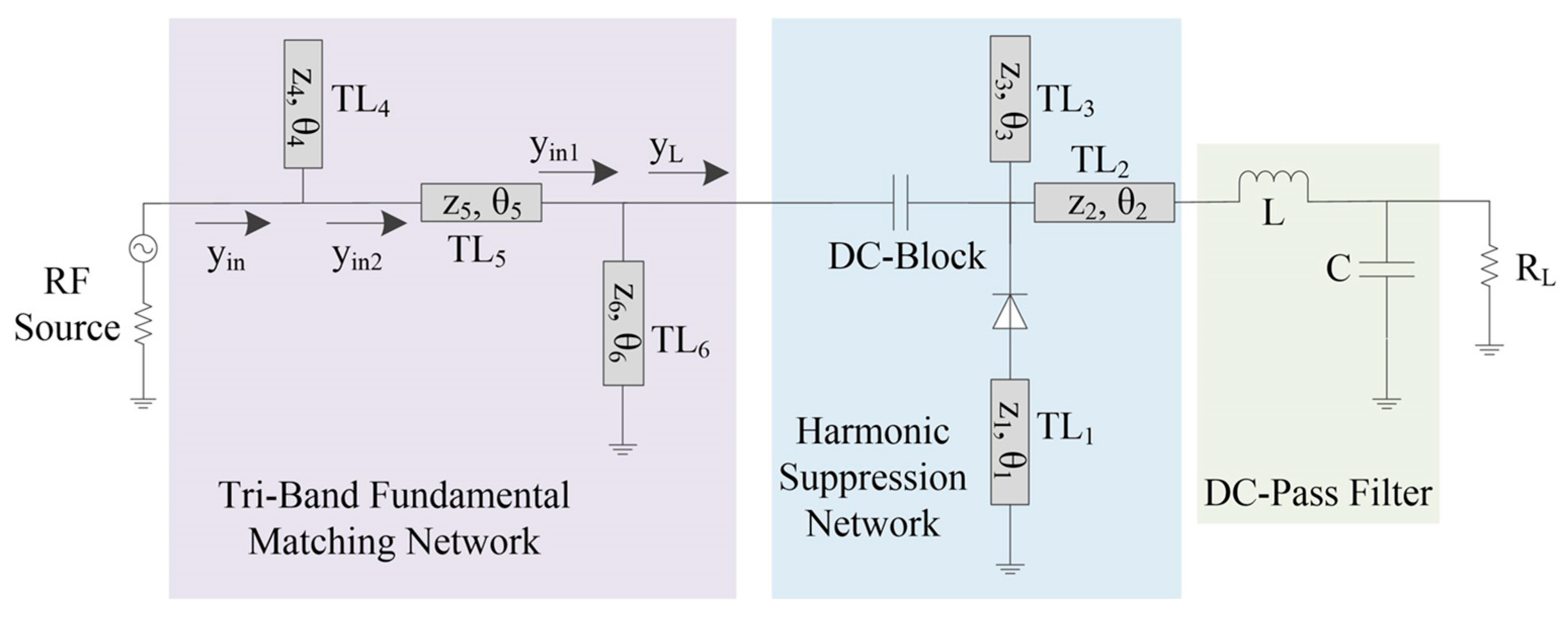
2. Design and Analysis of Tri-Band Rectifier
2.1. Design of Tri-Band Impedance Matching Network
2.2. Design of Harmonic Suppression Network
2.3. 2.45/3.5/5.8 GHz Tri-Band Rectifier Parameter Settings
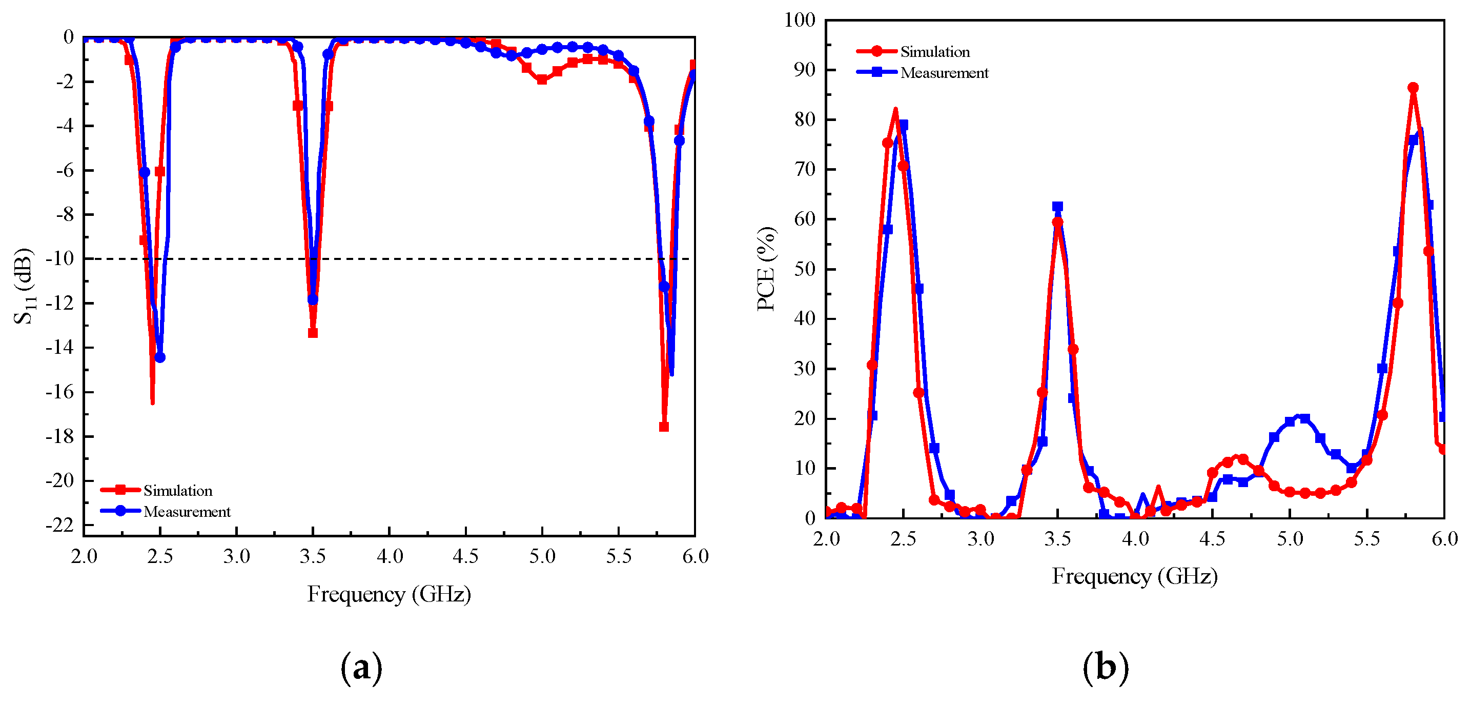
3. Results and Discussion
4. Conclusions
- Based on the theoretical analysis of closed-form equations, a new multiband IMN consisting of three TLINs is proposed, reducing the structural complexity by reducing the number of microstrip lines.
- This method achieves second harmonic suppression in all three frequency bands using only three TLINs. The HSNs are independent of the other parts, which reduces the interaction between the TLINs and simplifies the derivation process.
- The use of a single diode to achieve a three-band rectifier reduces the insertion loss of the structure.
- This design method achieves a high rectification efficiency while ensuring a compact structure.
- It enriches the design methodology of three-band rectifiers.
- At three frequencies, the input return loss of (|S11|) is less than −10 dB. The impedance matching performance of the structure is verified.
- At 200 Ω, the maximum PCE is 75.4%, 71.2%, and 80.9%, respectively.
- At three frequencies, a high PCE can be maintained over a wide input power range.
- The output voltage at the three frequencies is 3 V, which can effectively realize the power supply of small sensors.
- The measured structure size is 38 × 33, which is both efficient and compact compared with other studies. There is good agreement between the simulated and measured results.
Author Contributions
Funding
Data Availability Statement
Conflicts of Interest
References
- Brown, W.C. The history of power transmission by radio waves. IEEE Trans. Microw. Theory Tech. 1984, 32, 1230–1242. [Google Scholar] [CrossRef]
- Liu, C.; Lin, H.; He, Z.; Chen, Z. Compact patch rectennas without impedance matching network for wireless power transmission. IEEE Trans. Microw. Theory Tech. 2022, 70, 2882–2890. [Google Scholar] [CrossRef]
- Miwatashi, K.; Hirakawa, T.; Shinohara, N.; Mitani, T. Development of high-power charge pump rectifier for microwave wireless power transmission. IEEE J. Microw. 2022, 2, 711–719. [Google Scholar] [CrossRef]
- Wang, Q.; Dai, H.N.; Li, X.; Shukla, M.K.; Imran, M. Artificial noise aided scheme to secure UAV-assisted Internet of Things with wireless power transfer. Comput. Commun. 2020, 164, 1–12. [Google Scholar] [CrossRef]
- Liu, F.; Zhou, H.; Xia, L.; Chang, S.; Zhang, C.; Chen, J.; Tong, Y.; Cui, F.; Shen, Y.; Zhao, B.; et al. Body-based capacitive coupling and conductive channel power transfer for wearable and implant electronics. Nano Energy 2023, 115, 108761. [Google Scholar] [CrossRef]
- Makhetha, M.J.; Markus, E.D.; Abu-Mahfouz, A.M. Efficient wireless power transfer via self-resonant Conformal Strongly Coupled Magnetic Resonance for wireless sensor networks. Energy Rep. 2022, 8, 1358–1367. [Google Scholar] [CrossRef]
- Wu, P.; Huang, S.Y.; Zhou, W.; Yu, W.; Liu, Z.; Chen, X.; Liu, C. Compact high-efficiency broadband rectifier with multistage-transmission-line matching. IEEE Trans. Circuits Syst. II Express Briefs 2019, 66, 1316–1320. [Google Scholar] [CrossRef]
- He, Z.; Liu, C. A compact high-efficiency broadband rectifier with a wide dynamic range of input power for energy harvesting. IEEE Microw. Wirel. Compon. Lett. 2020, 30, 433–436. [Google Scholar] [CrossRef]
- Yang, F.Y.; Wang, D. IoT-enabled intelligent fault detection and rectifier optimization in wind power generators. Alex. Eng. J. 2025, 116, 129–140. [Google Scholar] [CrossRef]
- Almarri, N.; Chang, J.; Song, W.H.; Jiang, D.; Demosthenous, A. Piezoelectric energy harvesting and ultra-low-power management circuits for medical devices. Nano Energy 2024, 131, 110196. [Google Scholar] [CrossRef]
- Guo, J.; Zhu, X. Class-F rectifier RF-DC conversion efficiency analysis. In Proceedings of the 2013 IEEE MTT-S International Microwave Symposium Digest (MTT), Seattle, WA, USA, 2–7 April 2013. [Google Scholar] [CrossRef]
- Zeng, M.; Andrenko, A.S.; Liu, X.; Li, Z.; Tan, H.Z. A compact fractal loop rectenna for RF energy harvesting. IEEE Antennas Wirel. Propag. Lett. 2017, 16, 2424–2427. [Google Scholar] [CrossRef]
- Mendoza, J.; Sanchez, A. On the design of a RF Schottky diode rectifier for energy harvesting applications. In Proceedings of the 2018 IEEE International Autumn Meeting on Power, Electronics and Computing, Ixtapa, Mexico, 14–16 December 2018. [Google Scholar] [CrossRef]
- Abdallah, M.; Costantine, J.; Ramadan, A.H.; Tawk, Y.; Christodoulou, C.G. A new RF rectifier topology with enhanced operable power range. In Proceedings of the 2016 IEEE-APS Topical Conference on Antennas and Propagation in Wireless Communications, Cairns, QLD, Australia, 19–23 September 2016. [Google Scholar] [CrossRef]
- Surender, D.; Halimi, A.; Khan, T.; Talukdar, F.A.; Kishk, A.A.; Antar, Y.M.; Rengarajan, S.R. Semi-annular-ring slots loading for broadband circularly polarized DR-rectenna for RF energy harvesting in smart city environment. AEU-Int. J. Electron. Commun. 2022, 147, 154143. [Google Scholar] [CrossRef]
- Surender, D.; Halimi, M.A.; Khan, T.; Talukdar, F.A.; Koul, S.K.; Antar, Y.M.M. 2.45 GHz Wi-Fi band operated circularly polarized rectenna for RF energy harvesting in smart city applications. J. Electromagn. Waves Appl. 2022, 36, 407–423. [Google Scholar] [CrossRef]
- Li, C.; Ma, Z.H.; Chen, J.X.; Wang, M.N.; Huang, J.M. Design of a compact ultra-wideband microstrip bandpass filter. Electronics 2023, 12, 1728. [Google Scholar] [CrossRef]
- Surender, D.; Halimi, M.A.; Khan, T.; Talukdar, F.A.; Antar, Y.M.M. A 90° twisted quarter-sectored compact and circularly polarized DR-rectenna for RF energy harvesting applications. IEEE Antennas Wirel. Propag. Lett. 2021, 21, 1139–1143. [Google Scholar] [CrossRef]
- Liu, Z.; Zhong, Z.; Guo, Y.X. Enhanced dual-band ambient RF energy harvesting with ultra-wide power range. IEEE Microw. Wirel. Compon. Lett. 2015, 25, 630–632. [Google Scholar] [CrossRef]
- Rehman, M.; Ahmad, W.; Khan, W.T. Highly efficient dual band 2.45/5.85 GHz rectifier for RF energy harvesting applications in ISM band. In Proceedings of the 2017 IEEE Asia Pacific Microwave Conference, Kuala Lumpur, Malaysia, 13–16 November 2017. [Google Scholar] [CrossRef]
- Surender, D.; Halimi, M.A.; Khan, T.; Talukdar, F.A.; Antar, Y.M.M. Circularly polarized DR-rectenna for 5G and Wi-Fi bands RF energy harvesting in smart city applications. IETE Tech. Rev. 2021, 4, 880–893. [Google Scholar] [CrossRef]
- Tung, N. Multi-band ambient RF energy harvesting rectifier for autonomous wireless sensor networks. In Proceedings of the 2016 IEEE Region 10 Conference, Singapore, 22–25 November 2016. [Google Scholar] [CrossRef]
- Collado, A.; Daskalakis, S.; Niotaki, K.; Martinez, R.; Bolos, F.; Georgiadis, A. Rectifier design challenges for RF wireless power transfer and energy harvesting systems. Radioengineering 2017, 26, 411–417. [Google Scholar] [CrossRef]
- Yue, Z.; Xu, X.; Li, S.; Zhu, Y.H.; Lin, X.Q. Efficient and compact tri-band rectifier with large frequency ratio for WPT. IEEE Microw. Wirel. Compon. Lett. 2022, 32, 1355–1358. [Google Scholar] [CrossRef]
- Shen, S.; Chiu, C.Y.; Murch, R.D. A dual-port triple-band L-probe microstrip patch rectenna for ambient RF energy harvesting. IEEE Antennas Wirel. Propag. Lett. 2017, 16, 3017–3074. [Google Scholar] [CrossRef]
- Shen, S.; Zhang, Y.; Chiu, C.Y.; Murch, R. A triple-band high-gain multibeam ambient RF energy harvesting system utilizing hybrid combining. IEEE Trans. Ind. Electron. 2020, 67, 9215–9226. [Google Scholar] [CrossRef]
- Liu, Z.; Zhong, Z.; Guo, Y.X. High-efficiency triple-band ambient RF energy harvesting for wireless body sensor network. In Proceedings of the 2014 IEEE MTT-S International Microwave Workshop Series on RF and Wireless Technologies for Biomedical and Healthcare Applications, London, UK, 8–10 December 2014. [Google Scholar] [CrossRef]
- Chandravanshi, S.; Sarma, S.S.; Akhtar, M.J. Design of triple band differential rectenna for RF energy harvesting. IEEE Trans. Antennas Propag. 2018, 66, 2716–2726. [Google Scholar] [CrossRef]
- Liu, J.; Zhang, X.Y. Compact triple-band rectifier for ambient RF energy harvesting application. IEEE Access 2018, 6, 19018–19024. [Google Scholar] [CrossRef]
- Li, Z.; Zeng, M.; Tan, H.Z. A multi-band rectifier with modified hybrid junction for RF energy harvesting. Microw. Opt. Technol. Lett. 2018, 60, 817–821. [Google Scholar] [CrossRef]
- Tafekirt, H.; Sebastia, P.J.; Bouajaj, A.; Reda, B.M. A sensitive triple-band rectifier for energy harvesting applications. IEEE Access 2020, 8, 73659–73664. [Google Scholar] [CrossRef]
- Riaz, A.; Zakir, S.; Farooq, M.M.; Awais, M.; Khan, W.T. A triband rectifier toward millimeter-wave frequencies for energy harvesting and wireless power-transfer applications. IEEE Microw. Wirel. Compon. Lett. 2021, 31, 192–195. [Google Scholar] [CrossRef]
- Halimi, M.; Surender, D.; Khan, T.; Kishk, A.A.; Rengarajan, S.R. A multistepped transmission line matching strategy based triple-band rectifier for RFEH/WPT applications. IEEE Microw. Wirel. Compon. Lett. 2022, 32, 1007–1010. [Google Scholar] [CrossRef]
- Gyawali, B.; Thapa, S.K.; Barakat, A.; Yoshitomi, K.; Pokharel, R.K. Analysis and design of diode physical limit bandwidth efficient rectification circuit for maximum flat efficiency, wide impedance, and efficiency bandwidths. Sci. Rep. 2021, 11, 19941. [Google Scholar] [CrossRef]
- Gyawali, B.; Pokharel, R.K.; Thapa, S.K.; Aboualalaa, M.; Barakat, A.; Yoshitomi, K. Broadband and compact 3-bit digitally-controlled reconfigurable rectification circuit. In Proceedings of the Wireless Power Week, Bordeaux, France, 5–8 July 2022. [Google Scholar] [CrossRef]
- Nguyen, D.A.; Bui, G.T.; Nam, H.; Seo, C. Design of dual-band inverse class-F rectifier for wireless power transfer and energy harvesting. IEEE Microw. Wirel. Compon. Lett. 2023, 33, 355–358. [Google Scholar] [CrossRef]
- Wang, S.H.; Zheng, S.Y.; Leung, K.W.; Xia, M.H. A self-matched multi-band rectifier for efficient electromagnetic energy harvesting. IEEE Trans. Circuits Syst. I Regul. Pap. 2021, 68, 4556–4565. [Google Scholar] [CrossRef]
- Song, C.; Huang, Y.; Zhou, J.; Zhang, J.; Yuan, S.; Carter, P. A high-efficiency broadband rectenna for ambient wireless energy harvesting. IEEE Trans. Antennas Propag. 2015, 63, 3486–3495. [Google Scholar] [CrossRef]
- Nam, H.; Bui, G.T.; Nguyen, D.A.; Seo, C. A compact and high-efficiency 0.915/2.45/5.8 GHz triple-band rectifier with harmonic suppression based on coupled transmission line. IEEE Trans. Circuits Syst. II Express Briefs 2024, 71, 3553–3557. [Google Scholar] [CrossRef]


| TLIN | Length (mm) | Width (mm) |
|---|---|---|
| TL1 | 2.85 | 1.92 |
| TL2 | 14.99 | 7.20 |
| TL3 | 10.80 | 6.23 |
| TL4 | 18.66 | 9.06 |
| TL5 | 3.15 | 14.74 |
| TL6 | 12.84 | 1.21 |
| Reference | Freq. (GHz) | Size (mm2) | Diode | No. of Diodes | (%) |
|---|---|---|---|---|---|
| [24] | 0.915 | 29.5 × 21.3 | MA4E1317 | 3 | 72.6 |
| 2.45 | 71.8 | ||||
| 5.8 | 73.5 | ||||
| [31] | 0.9 | 54 × 42 | HSMS2852 | 3 | 52 |
| 1.8 | 50 | ||||
| 2.45 | 46 | ||||
| [33] | 1.95 | 36 × 22 | HSMS2860 | 1 | 65.5 |
| 2.7 | 62 | ||||
| 5.8 | 57.1 | ||||
| [37] | 1.78 | N/A | BAT15-03W | 3 | 60.1 |
| 2.35 | 71.4 | ||||
| 4.97 | 54.0 | ||||
| [26] | 1.85 | 44 × 81 | MA4E1317 | 1 | 48.0 |
| 2.15 | 52.0 | ||||
| 2.48 | 45.0 | ||||
| [38] | 1.85 | 32 × 32 | SMS7630 | 4 | 64.0 |
| 2.15 | 70.0 | ||||
| 2.45 | 60.0 | ||||
| [39] | 0.895 | 34 × 44 | BAT15-03W | 1 | 80.0 |
| 2.37 | 74.6 | ||||
| 5.57 | 73.6 | ||||
| This work | 2.45 | 38 × 33 | HSMS2860 | 1 | 75.4 |
| 3.5 | 71.2 | ||||
| 5.8 | 80.9 |
| Full Name | Abbreviation |
|---|---|
| Advanced Design System | ADS |
| Harmonic Suppression Network | HSN |
| Impedance Matching Network | IMN |
| Internet of Things | IoT |
| Internet of Vehicle | IoV |
| Industrial, Scientific and Medical | ISM |
| Power Conversion Efficiency | PCE |
| pseudomorphic High-Electron-Mobility Transistor | pHEMT |
| Radio Frequency Energy Harvesting | RFEH |
| Transmission Line | TLIN |
| Wireless Power Transfer | WPT |
Disclaimer/Publisher’s Note: The statements, opinions and data contained in all publications are solely those of the individual author(s) and contributor(s) and not of MDPI and/or the editor(s). MDPI and/or the editor(s) disclaim responsibility for any injury to people or property resulting from any ideas, methods, instructions or products referred to in the content. |
© 2025 by the authors. Licensee MDPI, Basel, Switzerland. This article is an open access article distributed under the terms and conditions of the Creative Commons Attribution (CC BY) license (https://creativecommons.org/licenses/by/4.0/).
Share and Cite
Liu, Y.; Xie, G. A Compact and High-Efficiency Design of Triple-Band Rectifier for Wireless Power Transfer. Electronics 2025, 14, 848. https://doi.org/10.3390/electronics14050848
Liu Y, Xie G. A Compact and High-Efficiency Design of Triple-Band Rectifier for Wireless Power Transfer. Electronics. 2025; 14(5):848. https://doi.org/10.3390/electronics14050848
Chicago/Turabian StyleLiu, Yan, and Gang Xie. 2025. "A Compact and High-Efficiency Design of Triple-Band Rectifier for Wireless Power Transfer" Electronics 14, no. 5: 848. https://doi.org/10.3390/electronics14050848
APA StyleLiu, Y., & Xie, G. (2025). A Compact and High-Efficiency Design of Triple-Band Rectifier for Wireless Power Transfer. Electronics, 14(5), 848. https://doi.org/10.3390/electronics14050848