Brief Report

Optimization of Cross-Bridge Kelvin Resistor (CBKR) Layout for the Precise Contact Resistance Measurement of TiSi2/n+ Si

Department of Electronic Engineering, Sogang University, Seoul 04107, Republic of Korea
*
Author to whom correspondence should be addressed.
Electronics 2025, 14(4), 762; https://doi.org/10.3390/electronics14040762
Submission received: 30 December 2024 / Revised: 1 February 2025 / Accepted: 13 February 2025 / Published: 15 February 2025

Abstract

:
This study investigates the impact of cross-bridge Kelvin resistor (CBKR) layout designs on specific contact resistivity (ρc) measurements between TiSi2 and n+ Si. The theoretical ρc is calculated as a function of silicon doping concentration (NSi) and Schottky barrier height (ϕb) to evaluate the measurement value. Various CBKR patterns are fabricated and measured with different contact hole areas (Ac) and aligned margins (δ) to evaluate measurement accuracy. The results show that CBKR with a narrow active width (W) can more accurately measure the ρc compared to the conventional layout mainly attributed to the current path confinement. In addition, if the contact hole length (L) is smaller than the transfer length (LT), the entire Ac contributes to the voltage drop of contact resistance (Rc), resulting in improved measurement accuracy. In contrast, if δ is increased, the measurement error decreases due to current dispersion near the recessed TiSi2 region, which is different from conventional CBKR layouts. Consequently, the measured ρc with an optimized layout shows a close value to the theoretical ρc.

1. Introduction

The metal–oxide–semiconductor field-effect transistors (MOSFETs) have evolved over the past several decades through miniaturization for better performance and higher integration density [1,2,3,4,5,6,7]. Conventionally, the current drivability of MOSFET is mainly determined by the channel resistance (Rch), and the other parasitic resistance (Rpara) such as a source/drain (Rsd), a contact (Rc), and a metal interconnect (Rm) can be ignorable. However, in the case of state-of-the-art short-channel MOSFET, the portion of Rpara in the total resistance (Rtot) is significantly increased because an aggressive scaling of channel length decreases the Rch, while the decrease in source/drain junction depth and contact area increases the Rsd and Rc (i.e., Rpara), respectively. Consequently, the proportion of Rpara in the total resistance has started to exceed Rch, with the Rc accounting for more than 50% of the Rpara [8,9,10,11]. Therefore, reducing the Rc has become increasingly important for improving MOSFET performance. Several strategies, such as a metal–insulator–semiconductor (MIS) contact [12], a silicidation [13], and doping engineering [14], have been suggested to reduce the Rc by decreasing a specific contact resistance (ρc). Among them, Ti silicidation is a promising technique since it can simultaneously achieve a high doping concentration [i.e., a low sheet resistance (Rsh)] with the help of dopant segregation and a low Schottky barrier height (SBH) [15,16,17,18].
In addition to the importance of reducing ρc, the significance of test patterns that can precisely evaluate the ρc increases, too. When the measurement range of ρc is below 10−7 Ω∙cm2, parasitic metal resistance and/or a current crowding effect cannot be ignored, leading to significant measurement errors. Therefore, the parasitic components of the test pattern should be minimized and eliminated. There are two representative test patterns for measuring Rc: the cross-bridge Kelvin resistor (CBKR) [19,20,21,22,23] and the transmission line model (TLM) [24,25,26]. The CBKR directly measures the ρc using its four-terminal structure, implying higher accuracy and simplicity [Figure 1a]. The TLM pattern determines the ρc by extrapolating the resistance and length. However, TLM requires complex modeling to extract ρc from total resistance measurements due to its high sensitivity to design and process parameters, which can introduce additional measurement errors during extrapolation.
In the CBKR, current is applied through the two terminals (I24) while voltage is measured across the other two terminals (V13). Rc is extracted using Ohm’s law; V13/I24 and ρc are calculated by multiplying the Rc by Ac (i.e., ρc = Rc · Ac). Although Rc can be calculated by using this one-dimensional (1-D) model, in practice, the additional voltage drops caused by current crowding near the contact hole can introduce measurement errors [19,20,21,22,23]. These errors become more pronounced when extracting a low ρc. There are several reports that the current crowding in CBKR can be suppressed by reducing the space between the contact hole and the active layer [19,20]. However, when the Ti silicidation is applied, it reduces the Rsh and changes the current distribution adjacent to the contact hole since it consumes the silicon and forms a recessed TiSi2 [Figure 1b,c]. Therefore, the current flows from the n+ Si region to the TiSi2 via the contact hole, resulting in a different layout dependency compared to the non-Ti silicidation case. Recently, Ti silicidation has emerged as a promising alternative to CoSi2 and Ni(Pt)Si in advanced CMOS technologies due to its low ρc [16,17,18]. Although various silicides have been studied using TLM patterns [25], to the best of our knowledge, there is no research on CBKR layouts considering the effects of Ti silicidation. Therefore, in this work, the various CBKR layouts are fabricated and analyzed to extract a precise ρc between TiSi2 and n+ Si.

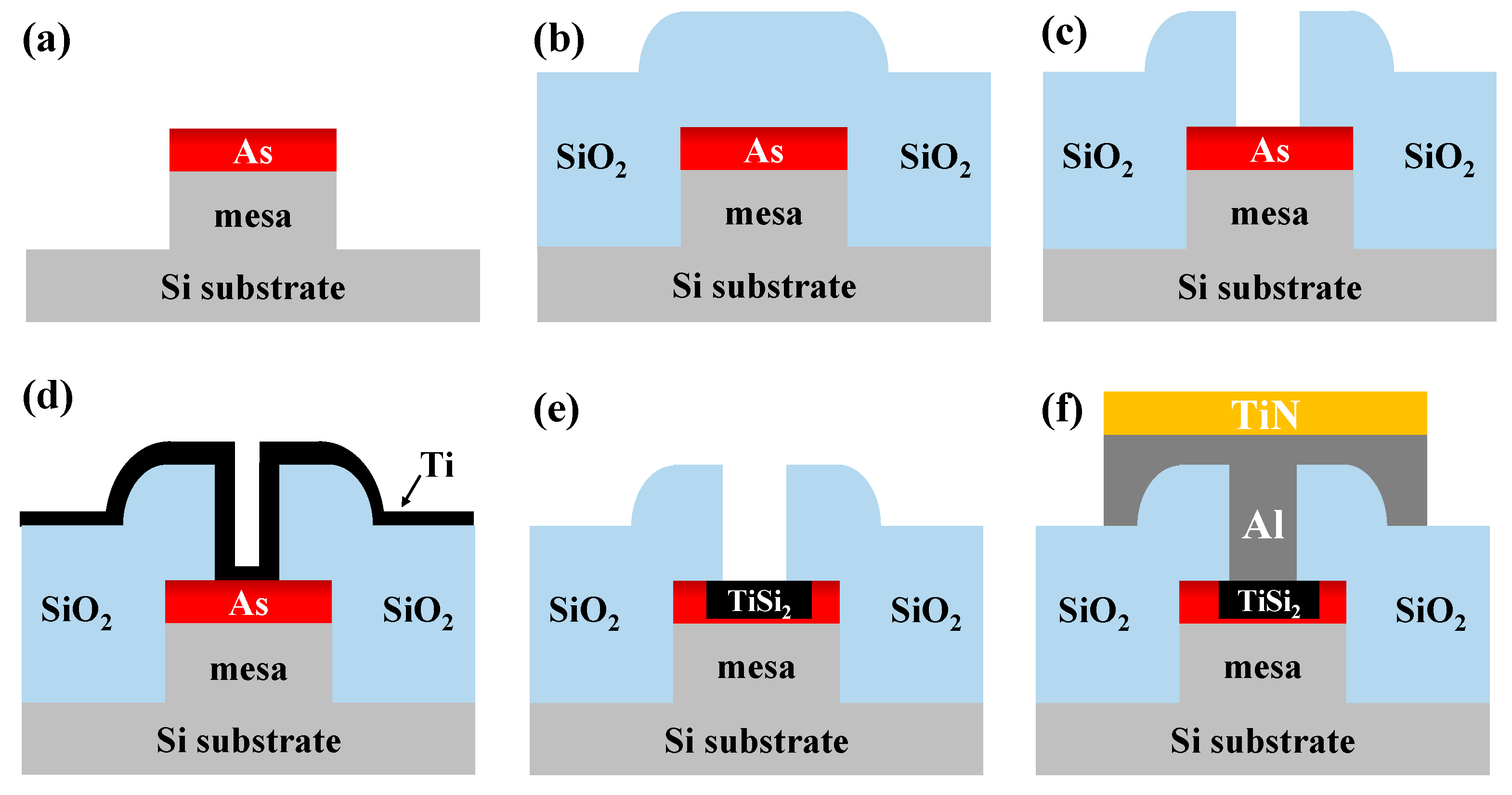
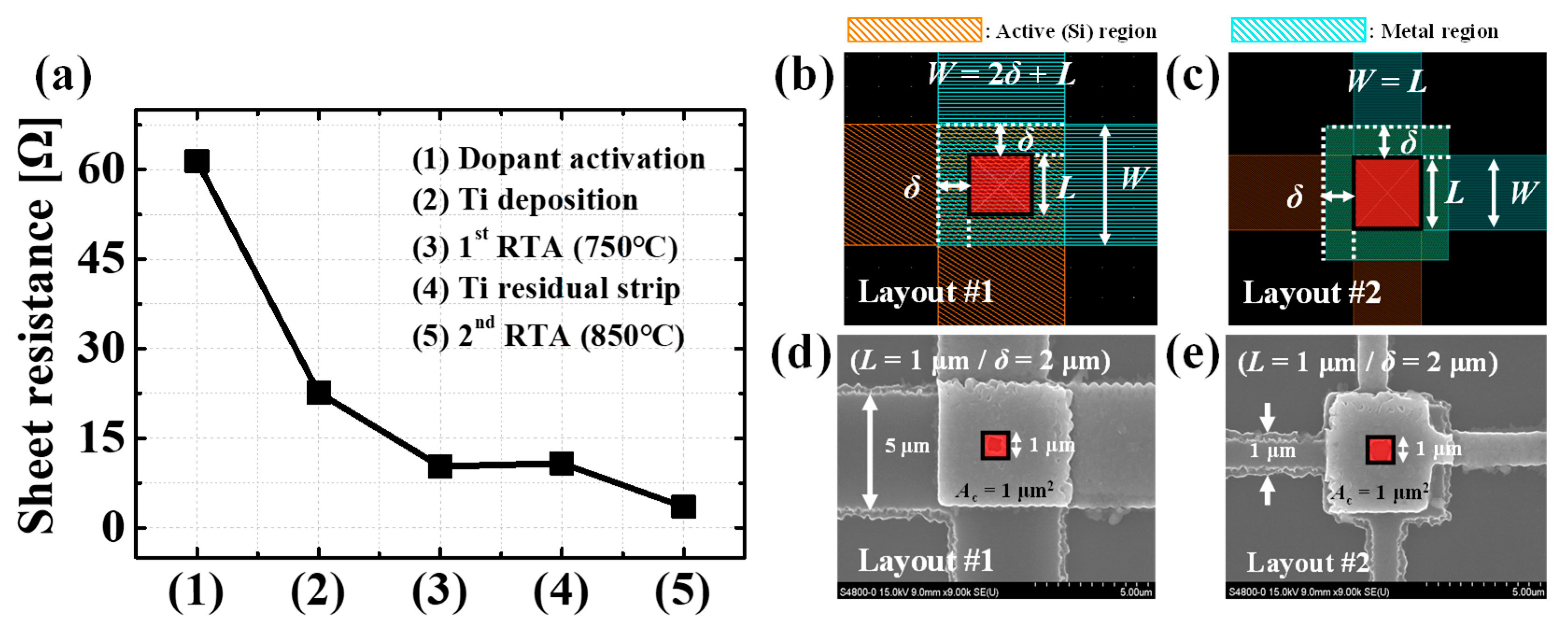
2. Fabrication Process

The CBKR test pattern is fabricated using a (100) low-doped p-type substrate. A 3 × 1020 cm−3-doped n-type region is formed by using an arsenic ion implantation (1 × 1015 cm−2-dose and 10 keV-acceleration energy), followed by a dopant activation at 1050 °C in an N2 atmosphere for 30 s with a rapid thermal annealing (RTA). It is patterned by photolithography and a Si reactive ion etching (RIE) for 1 µm depth to create a mesa pattern [Figure 2a]. A 400 nm-thick SiO2 is deposited using a plasma-enhanced chemical vapor deposition (PECVD), and a contact hole is patterned by the dry and wet etching process [Figure 2b,c]. After depositing a 30 nm-thick Ti with the help of a sputtering system [Figure 2d], two-step annealing processes are performed for a TiSi2 at the contact hole region. The first annealing is conducted at 750 °C for 30 s. Subsequently, an unreacted Ti is selectively removed using a sulfuric acid and hydrogen peroxide mixture (SPM, H2SO4:H2O2 = 4:1) at 120 °C for 20 min [Figure 2e]. The conditions for the second annealing are 850 °C and 30 s to convert the C-49 phase to the C-54 phase [27]. Figure 3a shows the Rsh of non-patterned arsenic-doped Si at each Ti silicidation step measured by a four-point probe. It is clear that the Rsh decreases as the processes proceed. As a back-end process, a 400 nm-thick Al and a 30 nm-thick TiN are sputtered on the substrate in sequence, followed by the patterning [Figure 2f]. Finally, a thermal annealing is performed at 400 °C for 30 s.
The CBKRs are fabricated in two different layouts. In the case of layout #1, an active width (W) is larger than the length of one side of a square-shaped contact hole (L) by a double align margin (δ) (i.e., W = L + 2δ) [Figure 3b]. On the other hand, layout #2 features the same W and L [Figure 3c]. Both layouts define the contact hole area (Ac) as a square of L (i.e., Ac = L2). The δ is identical along both the X and Y axes in layout #1 and layout #2. Figure 3d,e shows the plan-view scanning electron microscope (SEM) images for layouts #1 and #2 samples, respectively. In order to analyze the influence of pattern design, the various samples with the different L and δ are fabricated. The detailed information about design parameters is summarized in Table 1.

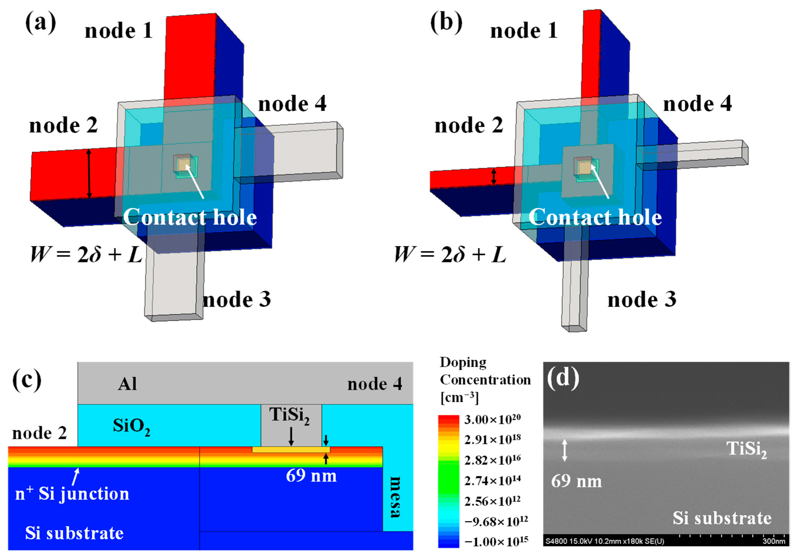
3. Simulation Structures and Extraction Condition

To analyze the measurement error related to the layout design, the technology computer-aided design (TCAD, Sentaurus™) simulations are performed. To account for omnidirectional current crowding, the three-dimensional (3D) structures are considered. Figure 4a,b shows the schematic view of 3D CBKR structures for layout #1 and layout #2, corresponding to the fabricated structures. Figure 4c shows the cross-sectional view (Y–Z plane) between nodes 2 and 4 at the center of the contact hole. Considering the ion implantation process conditions, the n+ Si junction exhibits a Gaussian doping profile with a peak doping concentration of 3 × 1020 cm−3 at the surface. A TiSi2 thickness is 69 nm, as shown in Figure 4d, which is 2.3 times thick at 30 nm; deposited Ti thickness. Last of all, the Al is used as the metal layer for nodes 3 and 4. The TiN on top of Al shown in Figure 2f is ignored for the simulation due to its negligible impact on contact resistance. To extract Rc in CBKR structures, I24 is swept from −40 μA to 40 μA in both simulation and measurement. In measurement, I24 is applied using the source measurement unit (SMU), while V13 is measured using the voltage measurement unit (VMU) of Keithley 4200A-SCS. Rc is extracted at current saturation points; I24 = ±40 μA.

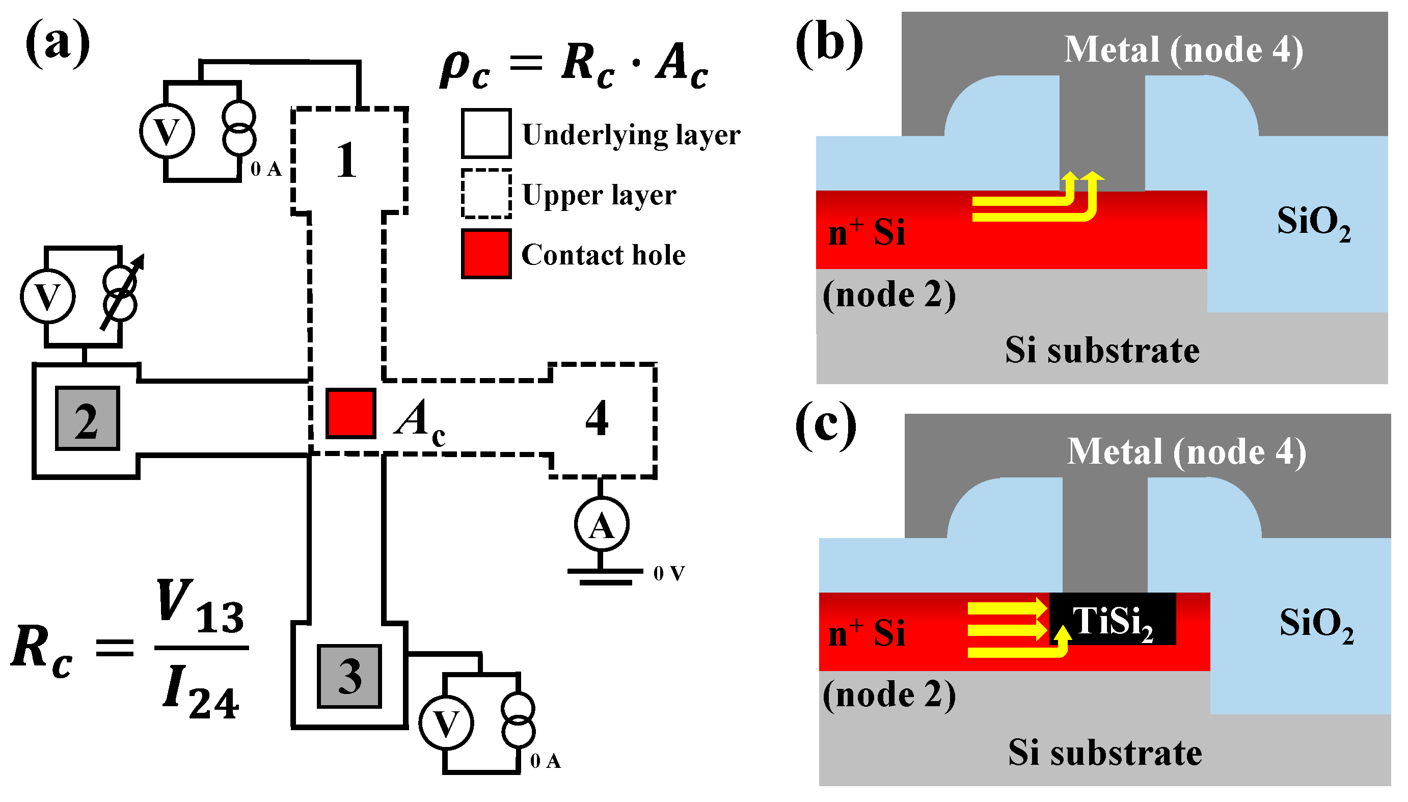
4. Theoretical ρc Calculation

The ρc between TiSi2 and n+ Si is theoretically calculated based on the doping concentration and Schottky barrier height (SBH, ϕb) to evaluate the measurement accuracy of the test patterns. If the doping concentrations exceed 5 × 1019 cm−3, a field emission dominates the tunneling process, and ρc is expressed as Equation (1) [28].
ρ c = k B sin π c 1 k T A * π q T exp q ϕ b E 00
Here, q, kB, T, εSi, and A* represent electron charge, Boltzmann constant, temperature, silicon permittivity, and the effective Richardson constant, respectively. The A* is 120 A∙cm−2∙K−2, where the effective mass (m*) is equal to the free electron mass (m0) [28]. The functions E00 and c1 describe the dependence of tunneling current on the temperature and doping concentration, which are expressed as Equations (2) and (3), respectively.
E 00 = q h 4 π N S i ε S i m t
c 1 = l n 4 q ϕ b E f 2 · E 00
The h, NSi, mt, and Ef represent the Plank constant, doping concentration of silicon, effective tunneling mass, and Fermi level of silicon, respectively. Here, mt is set to 0.19∙m0 [28]. Although an ideal SBH between TiSi2 and n-Si is 0.6 eV [29], it decreases due to a barrier lowering (Δϕb) caused by image force expressed as Equations (4) and (5) [30].
ϕ b = q E m a x 4 π ε S i
E m a x = 2 q N S i ψ S i ε S i
The Emax and ψSi represent the maximum electric field and surface potential at the silicon region, respectively. Based on Equations (1) to (5), Figure 5a,b shows the calculated Δϕb and ρc as a function of NSi, respectively. Considering NSi of the fabricated sample is ~3 × 1020 cm−3 (Figure 2), it corresponds to the 0.29 eV-Δϕb, resulting in a 0.31 eV effective ϕb in Equations (1) and (3) at the TiSi2/n+ Si interface. Consequently, the theoretical ρc is ~1.05 × 10⁻⁸ Ω∙cm2, which is used as a reference value for the evaluation of measurement results [Figure 5b].

5. Results and Discussion

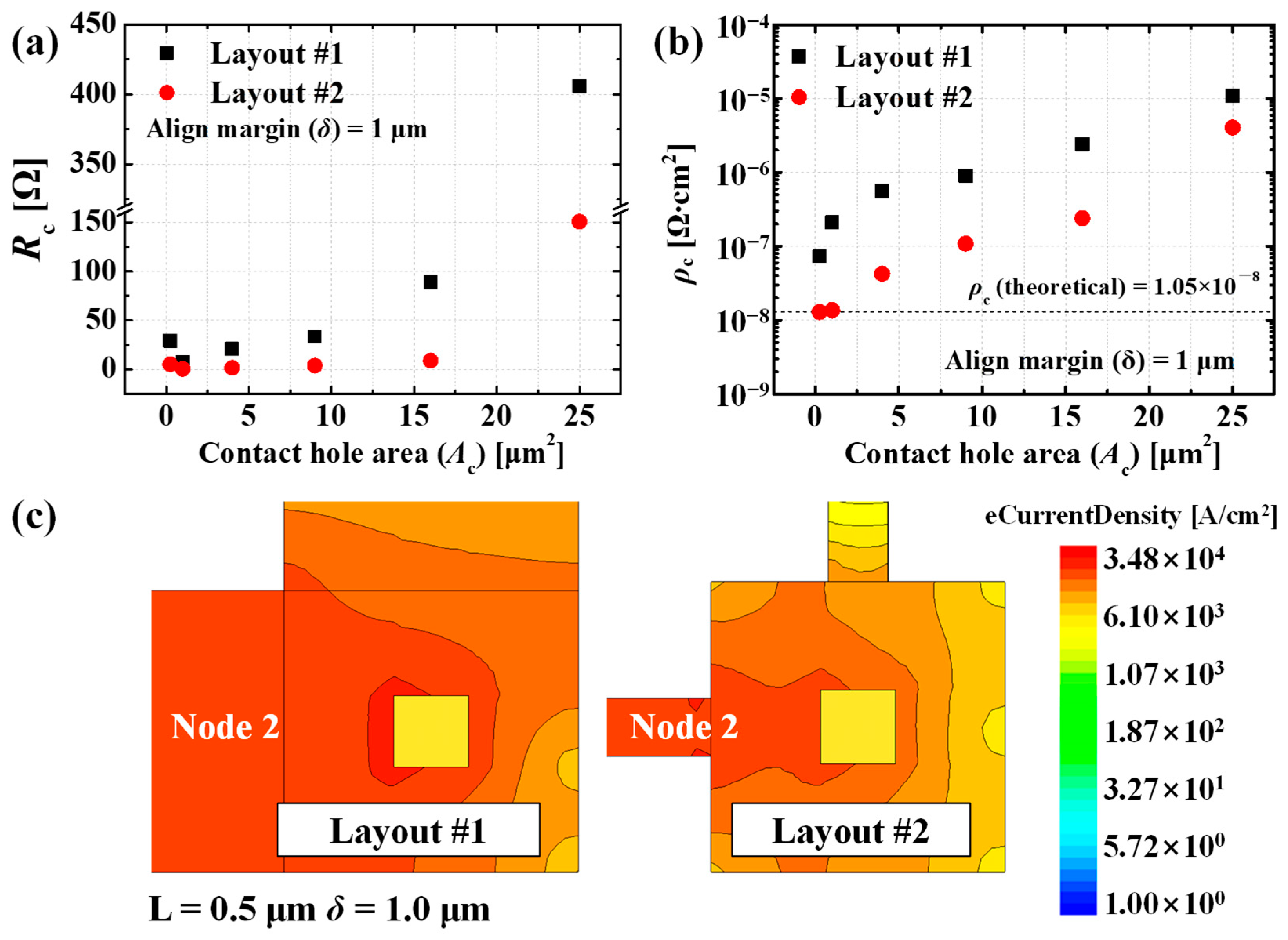
5.1. Layout Comparison

Figure 6a,b shows the measured Rc and ρc for layout #1 and #2 as a function of Ac with 1 μm- δ. The Rc of layout #2 is lower than that of layout #1 across all Ac, resulting in approximately an order of magnitude lower ρc compared to layout #1. The design parameters of layout #1 and #2 are identical, as shown in Table 1, except for the size of W. It indicates that a narrower W in layout #2 effectively constrains the current path, suppressing current crowding and decreasing the parasitic voltage drop in V13. Figure 6c shows the simulated plan-view current density distribution of both layouts, providing direct evidence of this improvement. Compared to layout #1, layout #2 confines the current path toward the contact hole, which leads to an accurate contact resistance measurement.

5.2. Contact Hole Area (Ac) Variation

Despite the improvement of measurement accuracy in layout #2, the measured ρc is much higher than the theoretical ρc at Ac above 1 μm2. On the other hand, the measured ρc is almost the same as the theoretical ρc when the Ac is less than 0.25 μm2 [Figure 6b]. In other words, the measurement errors significantly decrease with the smaller Ac. This result indicates that the actual area contributing to the Rc is smaller than the Ac for the large Ac, causing significant measurement errors during the ρc extraction. The current from n+ Si to TiSi2 does not flow uniformly across the Ac but flows toward the contact edge where the path resistance is lowest. The current density reduces away from the edge since the resistance consisting of Rsh and ρc along the contact hole increases. Therefore, the voltage drop V13 peaks at the edge and then exponentially decreases [Figure 7a]. This decay length, at which the voltage drop decreases to 1/e of its peak value, is defined as transfer length (LT) and determined by the ρc and Rsh (i.e., L T = ρ c / R s h ) [26]. Therefore, the effective contact hole area (Ac, eff), where the voltage drop V13 occurs, is expressed as the multiplication of LT and L (i.e., Ac, eff = LTL). Using the theoretical ρc and measured Rsh of TiSi2 [Figure 3a], LT is calculated to be 0.55 μm. For Ac-0.25 μm2, where L is smaller than LT, the voltage drop V13 occurs across the entire Ac. However, when L becomes larger than LT, the voltage drop V13 is confined within LT, causing measurement errors during ρc extraction [Figure 7b]. Therefore, L should be designed smaller than the LT to minimize the measurement errors caused by the mismatch between Ac and Ac, eff.

5.3. Align Margin (δ) Variation

Figure 8a shows the measured ρc as a function of δ for layouts #1 and #2 with Ac of 0.25 μm2. Layout #1 shows the measured ρc an order of magnitude higher than the theoretical ρc across all δ values due to the large W, which fails to constrain the current path, as discussed in Section 5.1. Layout #2 shows the measured ρc close to the theoretical ρc for δ from 3 μm to 1 μm. However, the measured ρc increases by an order of magnitude when δ decreases below 0.5 μm. This phenomenon is due to the recessed TiSi2 formation at the contact hole region. Figure 8b shows the simulated current density distribution for δ of 0.2 μm and 1 μm in layout #2. At δ of 0.2 μm, current concentrates within the narrow δ region, resulting in high current density near the recessed TiSi2 region. In contrast, at δ of 1 μm, current disperses over a wide δ region, exhibiting low current density near the recessed TiSi2 region. Although V13 should measure only the voltage drop at the contact interface, this high current density at the semiconductor region for small δ introduces additional parasitic voltage to V13, causing significant measurement errors. In contrast to the prior research showing that narrowing δ suppresses the current crowding and reduces measurement error [19], our results demonstrate that with Ti silicidation, narrowing δ increases the current crowding and measurement errors. While improved measurement accuracy is achieved at δ of 2 μm and 3 μm, the average value of measured ρc is most close to the theoretical ρc at δ of 1 μm. Also, considering layout area efficiency, a δ of 1 μm is optimal.

6. Conclusions

In this study, contact resistance measurements between TiSi2 and n+ Si are performed using various CBKR test pattern layout designs with evaluation of layout-dependent errors. The theoretical ρc is calculated to be ~1.05 × 10⁻⁸ Ω∙cm2 as a function of Nsi and Δϕb. A modified CBKR design with narrow W (layout #2) shows improvement in measurement accuracy compared to the conventional layout (layout #1) by confined current path. Investigation of Ac variations shows that accurate ρc extraction can be achieved when L is designed smaller than LT, as demonstrated with Ac-0.25 μm² since the entire Ac contributes to the voltage drop of Rc. Also, investigation of δ variations shows that recessed TiSi2 formation affects current distribution near the contact region. At δ of 1 μm, current disperses over a wide area, while at smaller δ, current concentrates near the recessed TiSi2 region, introducing parasitic voltage in V13 measurement. The optimized layout #2 with δ-1 μm and Ac-0.25 μm² achieves ρc measurements closely aligned with theoretical ρc, demonstrating the elimination of layout-dependent measurement errors between TiSi2 and n+ Si contact resistance characterization.

Author Contributions

Conceptualization, H.N. and S.K.; methodology, H.N., C.C., Y.J., and D.O.; validation, H.N.; investigation, H.N.; resources, H.N.; writing—original draft preparation, H.N.; writing—review and editing, S.K.; visualization, H.N.; supervision, S.K.; project administration, H.N.; funding acquisition, S.K. All authors have read and agreed to the published version of the manuscript.

Funding

This work was supported in part by the MOTIE (1415181069) and KSRC (20020830) support programs for the development of the future semiconductor device and in part by the Technology Innovation Program (20022821, Development of 532 nm Laser Thermal Processing Technology and Equipment Optimized for Semiconductor Process) funded by the MOTIE, Korea, and, in part, by National Research Foundation (NRF) of Korea funded by Ministry of Science and ICT under Grant NRF-2022R1A2C2092727 and, in part, by the MSIT, Korea, under the ITRC support program (IITP 2024-RS-2023-00260091) supervised by the IITP. The EDA tool was supported by the IC Design Education Center (IDEC), Korea.

Data Availability Statement

The data presented in this study are available in this article.

Conflicts of Interest

The authors declare no conflicts of interest.

References

  1. Schaller, R.R. Moore’s law: Past, present and future. IEEE Spectr. 1997, 34, 52–59. [Google Scholar] [CrossRef]
  2. Yu, B.; Chang, L.; Ahmed, S.; Wang, H.; Bell, S.; Yang, C.-Y.; Tabery, C.; Ho, C.; Xiang, Q.; King, T.-J.; et al. FinFET scaling to 10 nm gate length. In Proceedings of the 2002 International Electron Devices Meeting (IEDM), San Francisco, CA, USA, 8–11 December 2002; pp. 251–254. [Google Scholar]
  3. Yoon, J.-S.; Jeong, J.; Lee, S.; Baek, R.-H. Systematic DC/AC performance benchmarking of Sub-7-nm node FinFETs and nanosheet FETs. IEEE J. Electron. Devices Soc. 2018, 6, 942–947. [Google Scholar] [CrossRef]
  4. Wu, C.C.; Lin, D.W.; Keshavarzi, A.; Huang, C.H.; Chan, C.T.; Tseng, C.H.; Chen, C.L.; Hsieh, C.Y.; Wong, K.Y.; Cheng, M.L.; et al. High performance 22/20nm FinFET CMOS devices with advanced high-K/metal gate scheme. In Proceedings of the 2010 International Electron Devices Meeting (IEDM), San Francisco, CA, USA, 6–8 December 2010; pp. 27.1.1–27.1.4. [Google Scholar]
  5. Bae, G.; Bae, D.I.; Kang, M.; Hwang, S.M.; Kim, S.S.; Seo, B.; Kwon, T.Y.; Lee, T.J.; Moon, C.; Choi, Y.M.; et al. 3 nm GAA Technology featuring Multi-Bridge-Channel FET for Low Power and High Performance Applications. In Proceedings of the 2018 IEEE International Electron Devices Meeting (IEDM), San Francisco, CA, USA, 1–5 December 2018; pp. 28.7.1–28.7.4. [Google Scholar] [CrossRef]
  6. Jang, D.; Bury, E.; Ritzenthaler, R.; Bardon, M.G.; Chiarella, T.; Miyaguchi, K.; Raghavan, P.; Mocuta, A.; Groeseneken, G.; Mercha, A.; et al. Self-heating on bulk FinFET from 14nm down to 7nm node. In Proceedings of the 2015 IEEE International Electron Devices Meeting (IEDM), Washington, DC, USA, 7–9 December 2015; pp. 11.6.1–11.6.4. [Google Scholar]
  7. Mahapatra, S.; Sharma, U. A Review of Hot Carrier Degradation in n-Channel MOSFETs—Part II: Technology Scaling. IEEE Trans. Electron. Devices 2020, 67, 2672–2681. [Google Scholar] [CrossRef]
  8. AThean, A.V.; Yakimets, D.; Bao, T.H.; Schuddinck, P.; Sakhare, S.; Bardon, M.G.; Sibaja-Hernandez, A.; Ciofi, I.; Eneman, G.; Veloso, A.; et al. Vertical device architecture for 5nm and beyond: Device & circuit implications. In Proceedings of the 2015 Symposium on VLSI Technology (VLSI Technology), Kyoto, Japan, 16–18 June 2015; pp. T26–T27. [Google Scholar]
  9. Jung, S.-G.; Kim, J.-K.; Yu, H.-Y. Analytical Model of Contact Resistance in Vertically Stacked Nanosheet FETs for Sub-3-nm Technology Node. IEEE Trans. Electron. Devices 2022, 69, 930–935. [Google Scholar] [CrossRef]
  10. Thompson, S.E.; Parthasarathy, S. Moore’s law: The future of Si microelectronics. Mater. Today 2006, 9, 20–25. [Google Scholar] [CrossRef]
  11. Yeric, G. Moore’s law at 50: Are we planning for retirement? In Proceedings of the 2015 IEEE International Electron Devices Meeting (IEDM), Washington, DC, USA, 7–9 December 2015; pp. 1.1.1–1.1.8. [Google Scholar]
  12. Gupta, S.; Manik, P.P.; Mishra, R.K.; Nainani, A.; Abraham, M.C.; Lodha, S. Contact resistivity reduction through interfacial layer doping in metal-interfacial layer-semiconductor contacts. J. Appl. Phys. 2013, 113, 234505. [Google Scholar] [CrossRef]
  13. Adusumilli, P.; Alptekin, E.; Raymond, M.; Breil, N.; Chafik, F.; Lavoie, C.; Ferrer, D.; Jain, S.; Kamineni, V.; Ozcan, A.; et al. Ti and NiPt/Ti liner silicide contacts for advanced technologies. In Proceedings of the 2016 IEEE Symposium on VLSI Technology, Honolulu, HI, USA, 14–16 June 2016; pp. 1–2. [Google Scholar]
  14. Qiu, Z.; Zhang, Z.; Ostling, M.; Zhang, S.L. A Comparative Study of Two Different Schemes to Dopant Segregation at NiSi/Si and PtSi/Si Interfaces for Schottky Barrier Height Lowering. IEEE Trans. Electron. Devices 2008, 55, 396–403. [Google Scholar] [CrossRef]
  15. Yu, H.; Schaekers, M.; Peter, A.; Pourtois, G.; Rosseel, E.; Lee, J.G.; Song, W.-B.; Shin, K.M.; Everaert, J.-L.; Chew, S.A.; et al. Titanium Silicide on Si: P With Precontact Amorphization Implantation Treatment: Contact Resistivity Approaching 1 × 10⁻⁹ Ohm-cm2. IEEE Trans. Electron. Devices 2016, 63, 4632–4641. [Google Scholar] [CrossRef]
  16. Chew, S.A.; Yu, H.; Schaekers, M.; Demuynck, S.; Mannaert, G.; Kunnen, E.; Rosseel, E.; Hikavyy, A.; Dangol, A.; De Meyer, K.; et al. Ultralow resistive wrap-around contact to scaled FinFET devices by using ALD-Ti contact metal. In Proceedings of the 2017 IEEE International Interconnect Technology Conference (IITC), Hsinchu, Taiwan, 16–18 May 2017; pp. 1–3. [Google Scholar]
  17. Breil, N.; Lavoie, C.; Ozcan, A.; Baumann, F.; Klymko, N.; Nummy, K.; Sun, B.; Jordan-Sweet, J.; Yu, J.; Zhu, F.; et al. Challenges of nickel silicidation in CMOS technologies. Microelectron. Eng. 2015, 137, 79–87. [Google Scholar] [CrossRef]
  18. Mao, S.; Luo, J. Titanium-based ohmic contacts in advanced CMOS technology. J. Phys. D Appl. Phys. 2019, 52, 503001. [Google Scholar] [CrossRef]
  19. Stavitski, N.; Klootwijk, J.H.; van Zeijl, H.W.; Kovalgin, A.Y.; Wolters, R.A.M. Cross-Bridge Kelvin Resistor Structures for Reliable Measurement of Low Contact Resistances and Contact Interface Characterization. IEEE Trans. Semicond. Manuf. 2009, 22, 146–152. [Google Scholar] [CrossRef]
  20. Ono, M.; Nishiyama, A.; Toriumi, A. A simple approach to understanding measurement errors in the cross-bridge Kelvin resistor and a new pattern for measurements of specific contact resistivity. Solid-State Electron. 2002, 46, 1325–1331. [Google Scholar] [CrossRef]
  21. Kovalgin, A.Y.; Tiggelman, N.; Wolters, R.A.M. An Area-Correction Model for Accurate Extraction of Low Specific Contact Resistance. IEEE Trans. Electron. Devices 2012, 59, 426–432. [Google Scholar] [CrossRef]
  22. Holland, A.S.; Reeves, G.K.; Leech, P.W. Universal error corrections for finite semiconductor resistivity in cross-Kelvin resistor test structures. IEEE Trans. Electron. Devices 2004, 51, 914–919. [Google Scholar] [CrossRef]
  23. Loh, W.; Saraswat, K.; Dutton, R. Analysis and scaling of Kelvin resistors for extraction of specific contact resistivity. IEEE Electron. Device Lett. 1985, 6, 105–108. [Google Scholar] [CrossRef]
  24. Grover, S.; Sahu, S.; Zhang, P.; Davis, K.O.; Kurinec, S.K. Standardization of Specific Contact Resistivity Measurements using Transmission Line Model (TLM). In Proceedings of the IEEE 33rd International Conference on Microelectronic Test Structures (ICMTS), Edinburgh, UK, 4–18 May 2020; pp. 1–6. [Google Scholar]
  25. Stavitski, N.; Van Dal, M.J.; Lauwers, A.; Vrancken, C.; Kovalgin, A.Y.; Wolters, R.A. Evaluation of Transmission Line Model Structures for Silicide-to-Silicon Specific Contact Resistance Extrac-tion. IEEE Trans. Electron. Devices 2008, 55, 1170–1176. [Google Scholar] [CrossRef]
  26. Wu, Y.; Xu, H.; Gong, X.; Yeo, Y.C. A Ladder Transmission Line Model for the Extraction of Ultralow Specific Contact Resistivity—Part I: Theoretical Design and Simulation Study. IEEE Trans. Electron. Devices 2020, 67, 2682–2689. [Google Scholar] [CrossRef]
  27. Aldrich, D.B.; Chen, Y.L.; Sayers, D.E.; Nemanich, R.J.; Ashburn, S.P.; Öztürk, M.C. Stability of C54 titanium germanosilicide on a silicon-germanium alloy substrate. J. Appl. Phys. 1995, 77, 5107–5114. [Google Scholar] [CrossRef]
  28. Sze, S.M.; Ng, K.K. Physics of Semiconductor Devices, 3rd ed.; John Wiley & Sons: Hoboken, NJ, USA, 2006; pp. 79–124. [Google Scholar] [CrossRef]
  29. Aboelfotoh, M.O.; Tu, K.N. Schottky-barrier heights of Ti and TiSi2 on n-type and p-type Si(100). Phys. Rev. B. 1986, 34, 2311–2318. [Google Scholar] [CrossRef] [PubMed]
  30. Schroder, D.K. Semiconductor Material and Device Characterization, 3rd ed.; John Wiley & Sons: Hoboken, NJ, USA, 2005. [Google Scholar] [CrossRef]
Figure 1. (a) Measurement method of Rc using Ohm’s law in CBKR test pattern where Ac denotes the contact hole area. The current path of CBKR from node 2 to node 4 in case of (b) without and (c) with Ti silicidation. Due to Si consumption during Ti silicidation, recessed TiSi2 is formed and changes the current path.
Electronics 14 00762 g001
Figure 2. Process flow of cross-bridge Kelvin resistor (CBKR) test pattern with Ti silicidation. (a) Formation of n-type doped region (3 × 1020 cm−3) and mesa pattern via ion implantation and RIE, respectively. (b) SiO2 deposited by PECVD. (c) Contact hole formation through RIE and wet etching. (d) Ti metal deposition via sputtering. (e) TiSi2 formation by 2-step annealing process and unreacted Ti removal using SPM solution. (f) Back-end process for metal pad formation.
Electronics 14 00762 g002
Figure 3. (a) The Rsh of arsenic-doped Si measured at each Ti silicidation step. Two different layouts: (b) layout #1 (W = L + 2δ) and (c) layout #2 (W = L). The plan-view SEM images for the CBKR patterns with (d) layout #1 and (e) layout #2. Red rectangular represents the contact hole area.
Electronics 14 00762 g003
Figure 4. Schematic view of 3D CBKR structures in case of (a) layout #1 and (b) layout #2. The red and blue regions represent the n+ Si junction and Si substrate, respectively. Cross-sectional view of (c) 3D CBKR structure and (d) non-patterned TiSi2. The n+ Si junction shows Gaussian doping profile. The structures are shown for L and δ of 1 μm.
Electronics 14 00762 g004
Figure 5. (a) Calculated barrier lowering (∆Φb) as a function of NSi and (b) theoretical ρc incorporating the NSi.
Electronics 14 00762 g005
Figure 6. The measured (a) Rc and (b) ρc as a function of Ac for layouts #1 and #2. (c) The current density of layout #1 and #2 at I24 = 40 μA when L and δ are 0.5 and 1 μm, respectively. The current density near the contact hole is reduced in layout #2.
Electronics 14 00762 g006
Figure 7. (a) Equivalent circuit model showing resistance components (Rsh and ρc) and voltage drop V13 along the contact hole within LT. (b) Schematic comparison of contact area when L is larger than LT. The blue region indicates the Ac, eff contributing to voltage drop V13 while the gray region is not contributing.
Electronics 14 00762 g007
Figure 8. (a) The measured ρc when the Ac is 0.25 μm2 as a function of δ for layout #1 and #2. (b) Current density in case of layout #2 at I24 = 40 μA according to the δ. The current density within the δ region is more concentrated at δ-0.2 μm.
Electronics 14 00762 g008
Table 1. Design parameters of CBKR layout.
ParametersLayout #1Layout #2
Contact hole length (L)0.5/1/2/3/4/5 μm
Contact hole area (Ac)0.25/1/4/9/16/25 μm2
Align margin (δ)0.2/0.5/1/2/3 μm
Active (W)2δ + LL
Disclaimer/Publisher’s Note: The statements, opinions and data contained in all publications are solely those of the individual author(s) and contributor(s) and not of MDPI and/or the editor(s). MDPI and/or the editor(s) disclaim responsibility for any injury to people or property resulting from any ideas, methods, instructions or products referred to in the content.

