Article

Simulation Design of an Electron Gun for Microchannel Plate Scrubbing

1
Key Laboratory of Optoelectronic Devices and Systems of Ministry of Education and Guangdong Province, Shenzhen 518060, China
2
College of Physics and Optoelectronic Engineering, Shenzhen University, Shenzhen 518060, China
*
Author to whom correspondence should be addressed.
Electronics 2025, 14(3), 614; https://doi.org/10.3390/electronics14030614
Submission received: 6 January 2025 / Revised: 1 February 2025 / Accepted: 3 February 2025 / Published: 5 February 2025

Abstract

:
The microchannel plate (MCP) is susceptible to the adsorption of substantial amounts of gas during its fabrication process. To mitigate this, a uniform electron source is essential for effective electron scrubbing and gas removal. Thermionic emission, a method of electron generation, can be employed to create the electron source. In this study, a flat spiral filament was designed and simulated using the CST Studio Suite electron simulation software to assess the cleaning performance of the electron gun. The impact of variations in electron gun parameters on the uniformity of the electron beam and current density was systematically analysed. The simulation results show that, with filament, grid, focusing sleeve, and anode voltages set to 200 V, 500 V, 250 V, and 300 V, respectively, a uniform electron beam with a diameter exceeding 30 mm can be achieved. In order to obtain the current density (5~50 nA/mm2) required for the MCP, the temperature of the filament should be 1800–2000 K through theoretical calculation. These findings offer valuable insights for designing a more efficient electron gun for MCP scrubbing.

1. Introduction

The microchannel plate (MCP) is an electron multiplication device made of glass, commonly used in image intensifiers. It is known for its excellent characteristics, including small size, low noise, high electronic gain, and fast response, making it widely applicable in areas such as low-light night vision, gated imaging, medical diagnosis, and high-speed photography [1]. During MCP operation, electrons enter the channels from the input surface and are continuously accelerated by the parallel electric field generated by the electrodes at both ends. These electrons strike the inner walls of the channels, generating secondary electrons, thus achieving electron multiplication. However, residual gas left over from the manufacturing process can interact with multiplied electrons, leading to ion feedback and increased instability in secondary electron emission [2]. These residual gases contain water vapour and other gases; while the water vapour can be removed through high-temperature baking, excessive baking temperatures can soften or damage the MCP. Additionally, some gases cannot be entirely evacuated, and these residual gases may adhere to the photocathode surface during MCP operation, thereby reducing its sensitivity.
Electronic scrubbing uses a surface-emitting electron source to generate a uniform electron beam. When subjected to an electric field, the electron beam strikes the inner walls of the MCP channels, causing the gas adhered to these walls to be released, thus achieving a more thorough and uniform degassing effect [3]. To perform degassing on large-sized MCPs and improve the efficiency of the electron-cleaning process, it is essential to design an electron gun with a surface-emitting electron source capable of emitting a uniform electron beam over a large area and delivering the required current density. Cheng et al. developed an electron gun with a “V”-shaped filament [4]. The structure had a height of 20 mm and an outer diameter of φ35 mm, making it suitable for scrubbing MCPs with a diameter of φ30 mm. The design also allowed for adjustable current output during the degassing process. However, the study did not provide a detailed analysis of the uniformity of the generated surface electron source. Qiu et al. designed three types of filament shapes: conical spiral, flat spiral, and hemispherical [5]. By analysing the uniformity of thermal electrons emitted from the electron sources with different filament shapes, it was concluded that the surface uniformity of the flat spiral structure was superior. However, the experiment primarily focused on the greyscale values of the results, without providing specific uniformity measurements. Additionally, the study did not include an analysis of the flat spiral uniformity of the filament under varying parameters, such as filament width or the number of turns.
This study presents the design of an electron gun with a planar spiral filament structure, developed using the Particle Studio module in CST Studio Suite. The operational temperature range of the electron gun is determined by applying the current density calculation formula. Additionally, the simulation assesses the impact of various parameters—such as voltage across different structures and the temperature of the emission source—on the emitted current density. This analysis not only facilitates the generation of a uniform electron beam but also establishes the relationship between the emission source’s operating temperature and the emitted current density.

2. Simulation Model of Electron Gun

2.1. Thermionic Emission Theory

The velocities of free electrons within a metal follow a Fermi–Dirac distribution. Since the energy of the electrons is typically lower than the surface potential barrier, these free electrons are confined within the metal and it is difficult for them to escape from the surface. The minimum energy needed to surpass the barrier is known as the metal’s work function [6]. Thermionic emission is the most widely utilised electron emission method due to its advantages, such as high emitted current density, good stability, and relatively simple fabrication processes. The thermionic current density J e T can be approximated using the Richardson–Dushman thermal electron emission formula, as shown in Equation (1) [7]:
J e T = A T 2 exp W K T
where A denotes the theoretical value of the Richardson emission constant, T denotes the cathode temperature, W denotes the cathode work function, and K denotes the Boltzmann constant. According to Equation (1), primarily, two methods can be used modify the current density of thermionic emission. The first involves selecting different electron emission materials to adjust the work function, while the second involves varying the operating temperature.
Thermionic emission typically requires very high temperatures, which in turn necessitates the use of materials with high melting points. Tungsten, molybdenum, and tantalum are three metals commonly used as filaments for electron emission, and their properties are summarised in Table 1.
Tungsten has a high melting point, allowing filaments made from this material to withstand elevated temperatures. During the operation of the electron gun, the current passing through the tungsten filament was adjusted to achieve different operating temperatures. The high-temperature heating of the metal enables electrons to gain enough energy to overcome the surface potential barrier and escape from the metal surface [8]. Therefore, during the simulation process, varying the filament temperature results in different emission current densities.

2.2. Electron Gun Model

To achieve a uniformly emitting planar electron source, the flat spiral filament structure offers superior thermionic emission uniformity compared to other filament models [9]. Consequently, the filament was designed with a flat spiral configuration, as shown in Figure 1. The filament had a rectangular cross-section measuring 0.16 × 0.1 mm, with a pitch of 0.04 mm per turn. The overall diameter of the filament was 8 mm. It was positioned 8.9 mm from the bottom of the electron gun. An emission source was positioned on the surface of the filament to simulate electron emission when the filament was heated, and tungsten was selected as the material.
The grid was designed with a trumpet-shaped configuration, having a total length of 32 mm. The inner diameter at the inlet was φ10 mm, and the outer diameter was φ14 mm. At the outlet, the inner diameter ranged φ35–φ36 mm, and the outer diameter ranged φ37–φ38 mm. Within this range, the resulting electron beam diameter can exceed 30 mm, which is sufficient for large-scale scrubbing of the microchannel plate without requiring multiple cleaning cycles, thus reducing time-related costs. Furthermore, the electron beam diameter remains below 38 mm, ensuring that the current density does not become excessively low and simplifying the design of subsequent components [10]. In this study, inner and outer diameters of φ35.6 mm and φ37.6 mm, respectively, were selected within this range.
A focusing pole with an inner diameter of φ35.6 mm, an outer diameter of φ37.6 mm, and a length of 27 mm was positioned 1 mm behind the grid to focus the electron beam [11]. A 1-mm thick non-conductive barrier ring was placed between the grid and focusing pole, allowing the grid and the focusing pole to be biased at different voltages. Finally, an anode receiving surface with a diameter of φ37.6 mm was positioned 70 mm from the focusing pole to collect the electrons.
The cross-sectional view of the electron gun, modelled in CST Studio Suite, is shown in Figure 2. The structure consists of four components: the filament, grid, focusing pole, and anode. Based on the configuration of these components, the overall length of the electron gun was set to 130 mm.
The boundary of the flat spiral filament exhibited considerable variation; however, the temperature in the central region remained highly uniform, resulting in excellent surface uniformity. When a voltage was applied to both ends of the filament, it began to heat up. Once it reached a certain temperature, electrons were emitted. By applying a high voltage to the electron input surface of the MCP relative to the filament, the emitted electrons were directed toward the MCP input surface under the influence of the electric field. By carefully adjusting the voltages across the various components, the size of the electron beam incident on the MCP input surface could be controlled, achieving a uniform electron beam distribution with a diameter greater than 30 mm [12].

3. Simulation Results and Discussions

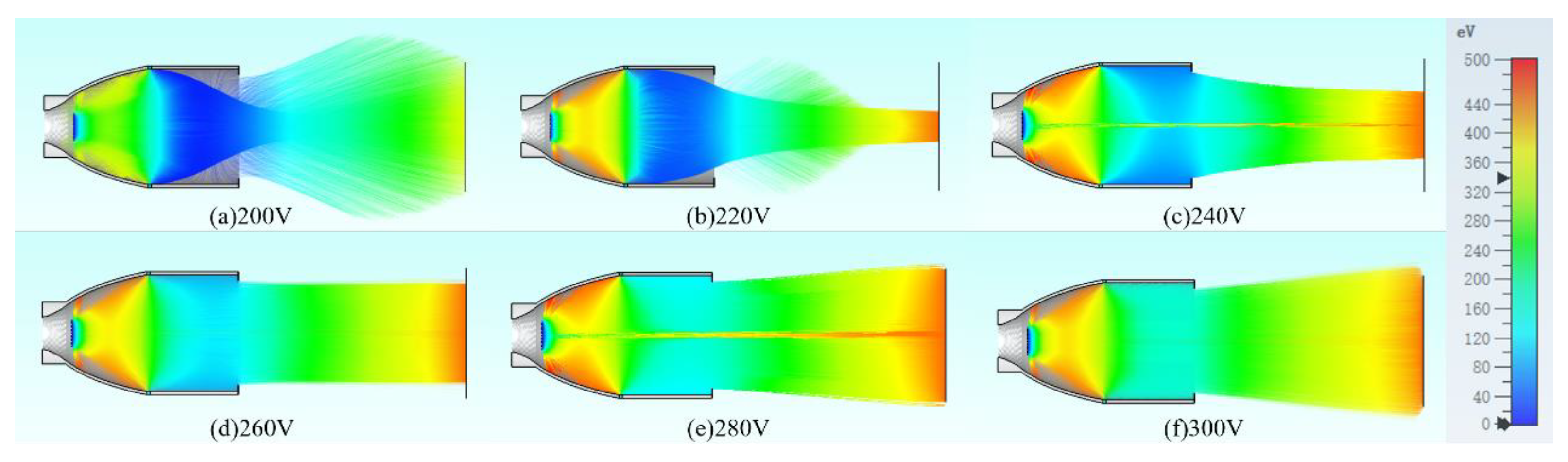
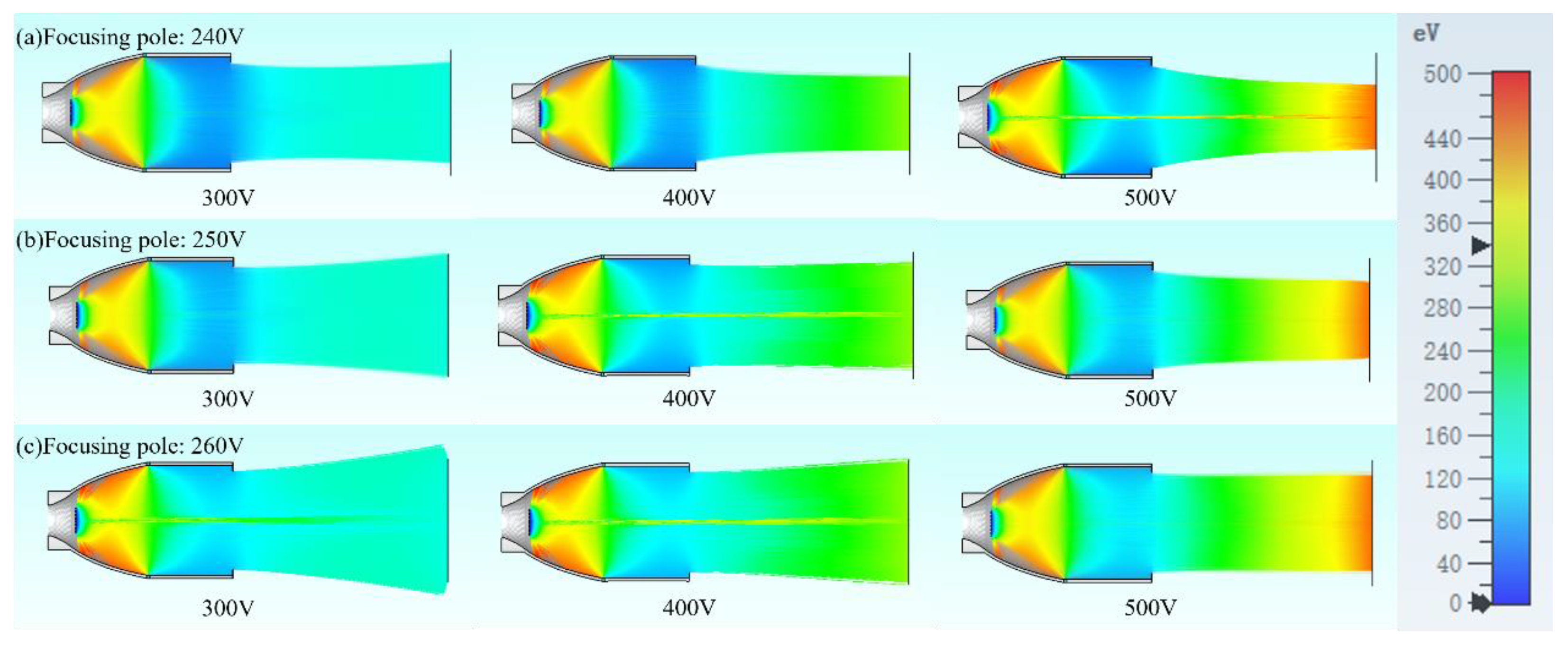
3.1. Effects of Focusing Pole Voltage and Anode Voltage on Electron Trajectory

In this electron gun simulation model, to mitigate the risks associated with high voltage and prevent potential damage to the microchannel plate from excessively high energy in the emitted electron beam, the voltage of each component was maintained within 50–500 V [13]. The reference point for the various voltage described in this paper is the voltage of the filament. Since electrons were emitted from the filament, the voltages of other structures were set with the filament voltage as the reference point, thereby achieving the purpose of diverging, focusing, and receiving the electron beam. Specifically, the filament voltage was set to 200 V, while the voltages of the grid structure and anode were both adjusted to a maximum of 500 V. This configuration helped to disperse the electrons emitted from the filament within the electric field, thereby increasing the electron distribution area. By varying the focusing sleeve voltage from 200 V to 300 V in increments of 20 V, different electron trajectories were achieved, as shown in Figure 3.
As illustrated in Figure 3, the electron beam, originating from the filament, first underwent diffusion within the grid structure, followed by convergence within the focusing sleeve, and was finally emitted toward the anode. Upon examining the electron trajectories under varying focusing voltages, it was observed that at lower focusing voltages, the electrons primarily converged at the centre of the anode. As the focusing voltage increased, the electrons gradually spread outward [14].
Since the diffusion of the electron beam increased when the anode voltage was reduced, the focusing sleeve voltage can be set to 240 V, 250 V, and 260 V, respectively. Meanwhile, the anode voltage can be adjusted from 300 V to 500 V to obtain different electron motion trajectories, as shown in Figure 4.
As depicted in Figure 4b, when the focusing sleeve was set to 250 V, the electron trajectories emitted from the focusing sleeve and reaching the anode transition from diffusion to focusing as the anode voltage changed. When the anode voltage exceeded 400 V, the electrons emitted from the electron gun no longer diffused effectively, resulting in a smaller area for the emitted electron beam. To achieve a larger and more uniform electron beam distribution, it was necessary to adjust the anode voltage. Hence, the most optimal voltage configuration was as follows: a filament voltage of 200 V, a grid voltage of 500 V, a focusing sleeve voltage of 250 V, and an anode voltage varying between 300 V and 400 V. The voltages of the various components could be adjusted proportionally [15], resulting in an electron beam distribution with a diameter greater than 30 mm at the anode.
The particle distribution plot and the corresponding histogram of the electron beam at the anode were generated using the electromagnetic simulation software CST Studio Suite, as shown in Figure 5. The particle distribution plot illustrates the two-dimensional positions of the penetration points where particles impacted the surface of the monitor, represented in absolute coordinates. The particle distribution histogram shows the normalised number of particles passing through the monitor surface at specific particle positions [16].
As shown in Figure 5, the electron density was significantly higher at both the centre and edges compared to other regions. This was because the central portion of the flat spiral filament emitted more electrons, which were more effectively directed toward the centre of the anode than those emitted from other areas. Additionally, the voltage difference between the focusing pole and the anode caused the electrons to spread toward the edges, resulting in higher electron density in these regions. From Figure 5c, the electron density variation within a 30 mm diameter range at the anode was found to be 0.019985.
To achieve a more uniform electron beam distribution within a 30 mm diameter range, this study explored two approaches. The first involved removing the central portion of the filament to reduce the electron density in the centre of the beam [17]. The second approach involved adjusting the anode voltage to ensure that the electron beam diffused toward the edges and extended beyond the 30 mm diameter, thereby resulting in a more uniform distribution within the 30 mm range.
As shown in Figure 6, after hollowing out the central radius of 0.4 mm in the original filament model, the electron beam was no longer focused at the centre. This resulted in a more uniform particle distribution. The electron density difference between the two filament models was calculated within a 30 mm diameter range. For model 2, the electron density difference was found to be 0.013711. Comparing this with the electron density difference for model 1, it could be observed that the overall uniformity of the particle distribution of the electron beam in model 2 improved by 31.40%.

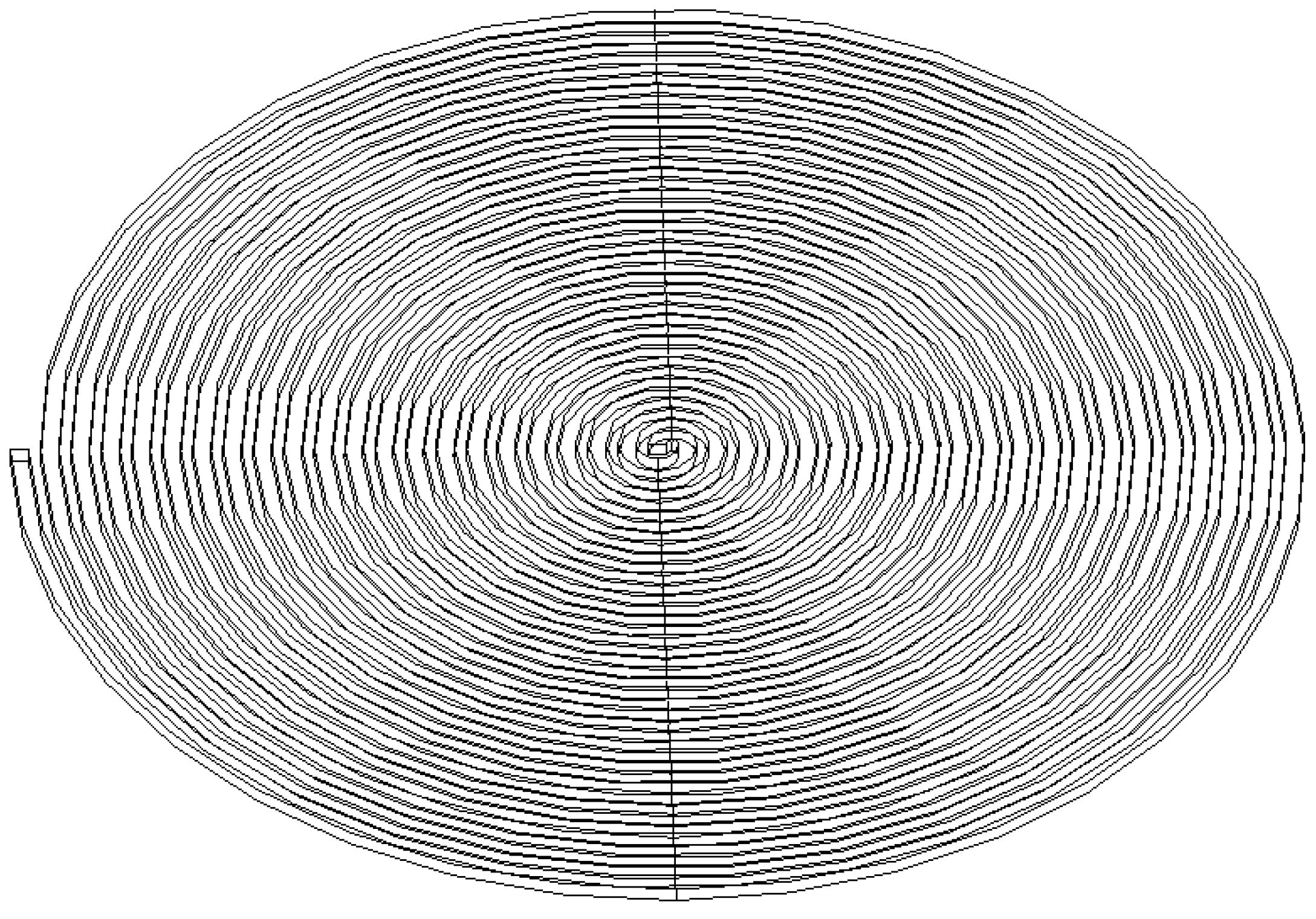
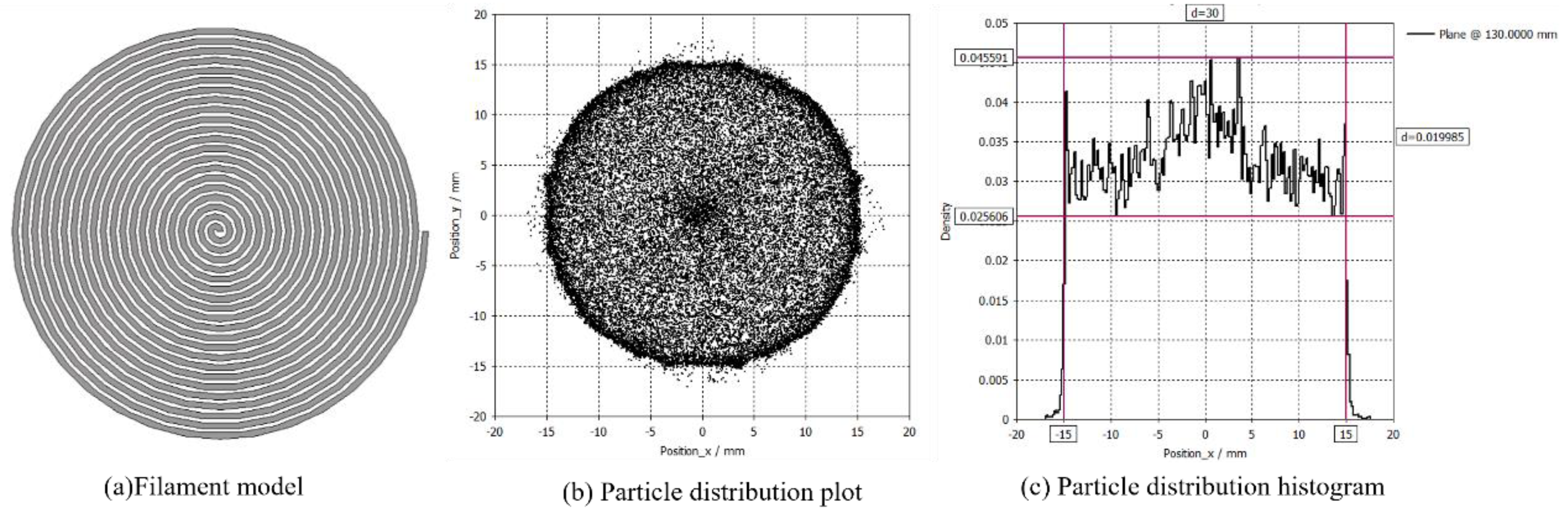
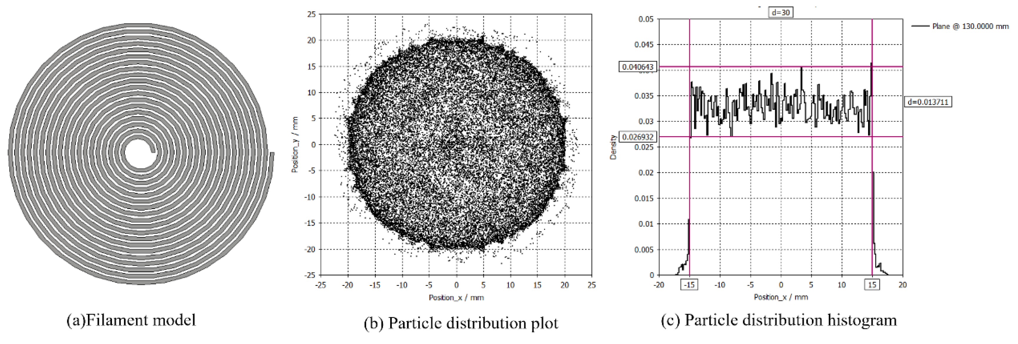
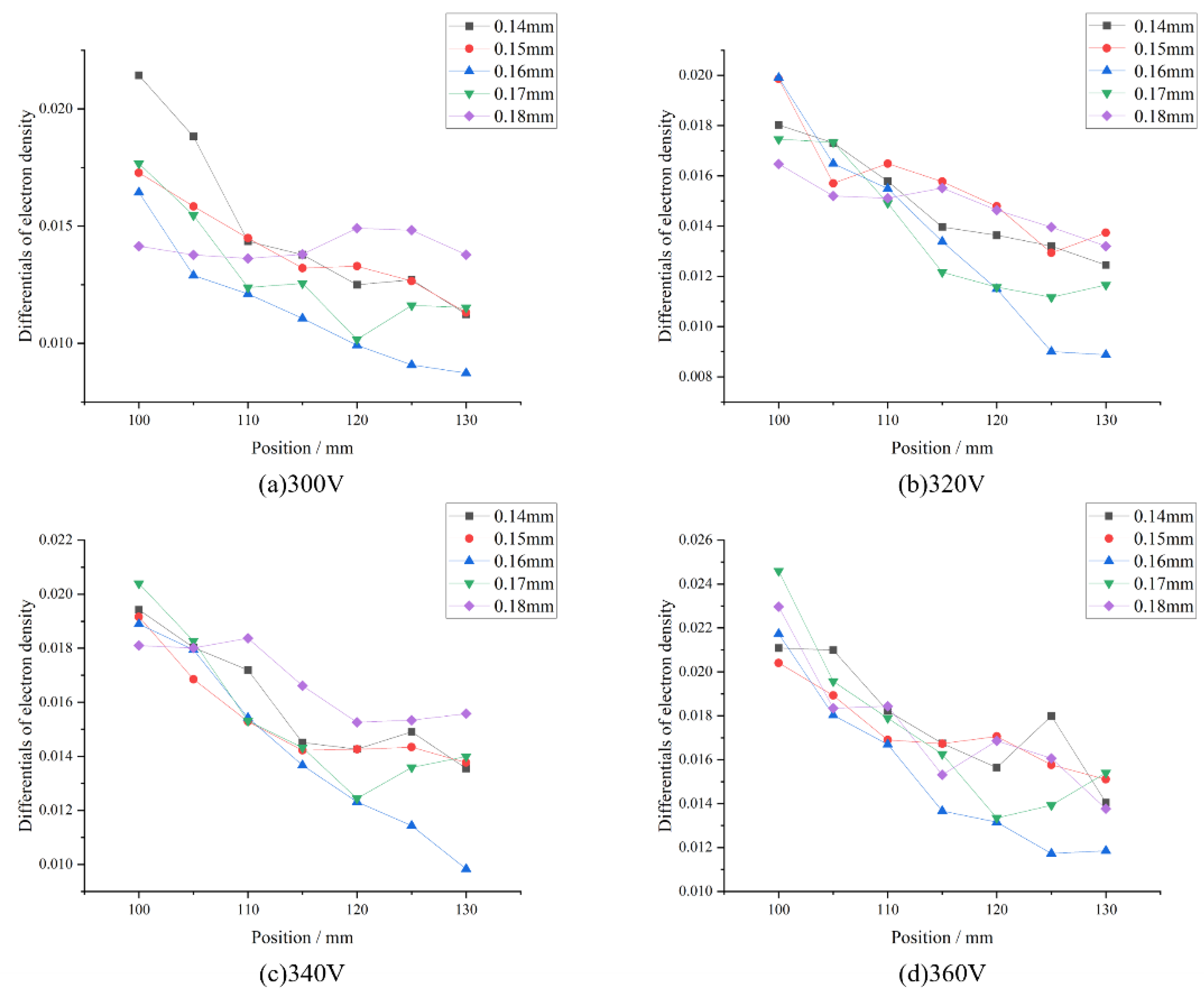
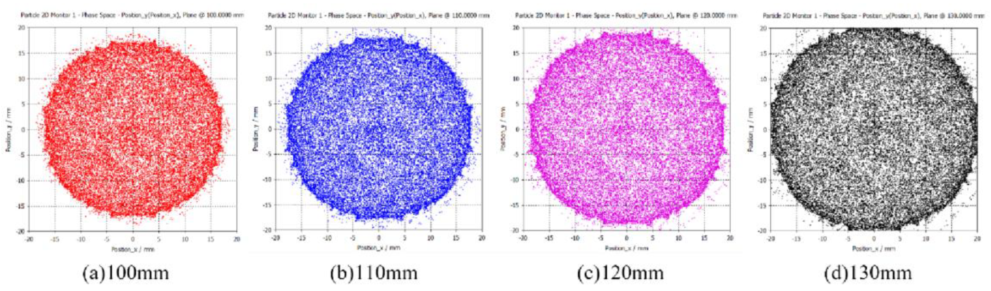
3.2. Effect of Filament Width on Electron Beam Uniformity

The electron gun designed in this study required an adjustable range of at least 30 mm from the exit to the anode to ensure a uniform electron beam within this range. This design facilitated effective scrubbing of the microchannel plate at various positions within the specified range. The anode voltage was incrementally set to 300 V, 320 V, 340 V, and 360 V, with a 2D monitor positioned between 100 mm and 130 mm from the bottom of the electron gun. Using the filament model, the filament width was varied in steps of 0.01 mm within the range of 0.14–0.18 mm. This resulted in corresponding filament areas of 39.276 mm2, 42.082 mm2, 44.887 mm2, 47.693 mm2, and 50.498 mm2. The particle counts of 78,552, 84,163, 89,774, 95,385, and 100,996 were adjusted to maintain a constant electron emission density. The relationship between the variation in electron beam density and filament width after processing the particle distribution is depicted in Figure 7.
As shown in Figure 7, the uniformity of the electron beam emitted from the electron gun was influenced by the electron emission area of the filament, but not in a direct proportional relationship. When the electron emission density was kept constant, if the filament width was less than 0.16 mm, an increase in filament width resulted in a larger emission area, causing more electrons to be directed toward regions with lower electron density due to the influence of the electric field. This ultimately reduced the variation in electron density and improved the uniformity of the electron distribution. When the filament width exceeded 0.16 mm, the variation in the number of electrons in the dense region was greater than that in the sparse region, resulting in an increase in the overall variation in electron density.
When the filament width was 0.16 mm, the electron density variation in the particle distribution at a distance of 130 mm was minimised, with values of 0.00873, 0.00887, 0.00983, and 0.01185. At this point, the emitted electron beam was the most uniform, with an anode voltage of 300 V, yielding an electron density variation of 0.00873. Compared with the initial electron beam, the overall uniformity of the particle distribution increased by 56.32%.
With an anode voltage of 300 V and a filament width of 0.16 mm, particle distribution diagrams at distances of 100 mm, 110 mm, 120 mm, and 130 mm from the bottom of the electron gun are presented in Figure 8. As shown, the designed electron gun offered an adjustable range of 30 mm for the emitted electron beam. Within this range, a uniform electron distribution was maintained over a 30 mm diameter area.

3.3. Effect of Filament Temperature on Output Current Density

The electron gun emitter was made of tungsten, with a work function of 4.54 eV. The voltages applied to the filament, grid, focusing sleeve, and anode were set to 200 V, 500 V, 250 V, and 300 V, respectively, with the filament width fixed at 0.16 mm. Using the Richardson–Dushman equation, the filament temperature was varied within 1800–2000 K. The emission current density was measured for each temperature setting, and the resulting relationship between current density and temperature is shown in Figure 9.
As shown in Figure 9, when the filament operating temperature varied between 1800 K and 2000 K, the emission current density of the electron gun increased exponentially, ranging from 5 to 50 nA/mm2. This trend is in agreement with the results obtained from the gain model found in the literature [18]. Prior to scrubbing the MCP, the filament current was adjusted to achieve the corresponding operating temperature within the simulation range. The resulting emission current density fell within this range, providing an electron flux sufficient to meet the cleaning requirements of the MCP.

4. Conclusions

In conclusion, the uniformity of the electron gun was influenced by the focusing voltage, anode voltage, and filament design. Keeping other parameters constant, the voltages for the filament, grid structure, and focusing sleeve were set to 200 V, 500 V, and 250 V, respectively, while the anode voltage was varied between 300 V and 400 V to maintain a consistent emission diameter of 30 mm. The filament was designed as a flat spiral with a width of 0.16 mm and an overall diameter of 8 mm, with the central region (radius 0.4 mm) hollowed out. This configuration resulted in the highest uniformity of the emitted electron beam, achieving a 56.32% improvement in uniformity as compared to the original filament model. Additionally, when the filament operating temperature varied between 1800 K and 2000 K, the emission current density increased exponentially within the range of 5 to 50 nA/mm2 as the temperature increased. By adjusting the filament current to achieve different temperatures, corresponding emission current densities were obtained, enabling the effective cleaning of the microchannel plate.

Author Contributions

Conceptualization/supervision: J.Z.; methodology/writing—original draft preparation: Z.Y. and Y.X.; writing—review and editing: Z.Y. and J.Z.; formal analysis: Z.Y.; funding acquisition: J.Z. All authors have read and agreed to the published version of the manuscript.

Funding

This paper was funded by the National Natural Science Foundations of China (NSFC) (No. 12175153, No. 11805137).

Data Availability Statement

The data in this article were simulated using CST studio suite software. If readers need it, the author can provide it to them as appropriate.

Conflicts of Interest

The authors declare no conflicts of interest.

References

  1. Cui, D.X.; Zheng, S.C.; Qiu, Y.F.; Qian, Y.S.; Chang, B.K. Effect of Electron Rinse on Output SNR and Electron Gain of the Microchannel Plates. Acta Photonica Sin. 2012, 41, 962–966. [Google Scholar]
  2. Hui, L.; Liu, F.; Zhang, L.D.; Gao, X.; Miao, Z.; Niu, S.; Wang, L.; Zhang, X.H. Study on electron scrubbing methods of Cs2Te ultraviolet double-MCP image intensifiers. In Proceedings of the International Symposium on Photoelectronic Detection and Imaging 2013: Low-Light-Level Technology and Applications, Beijing, China, 25–27 June 2013. [Google Scholar]
  3. Lian, J.; Sun, Y.; Zhang, X.; Feng, Y.; Bo, T.; Xu, T.; Shi, X.; Cai, H.; Liu, H. Effect of electron scrubbing on gain and dynamic range of microchannel plate. In Optical Sensing and Imaging Technologies and Applications; SPIE: Bellingham, WA, USA, 2018. [Google Scholar]
  4. Cheng, H.C.; Shi, F.; Hou, Z.P.; Shi, H.L.; Shi, P.F. Design of electron gun for scrubbing microchannel plate. J. Appl. Opt. 2007, 28, 582–586. [Google Scholar]
  5. Qiu, Y.F.; Chang, B.K.; Zhang, J.J.; Tian, S.; Fu, R.G. Area Source Filament Thermion Emission Flow Density And Uniformity Analysis. Acta Armamentarii 2009, 30, 617–621. [Google Scholar]
  6. Xue, Z.Q. Electron Emission and Electron Spectroscopy; Peking University Press: Beijing, China, 1993. [Google Scholar]
  7. Martin, R. Theory and Design of Charged Particle Beams, 2nd ed.; WILEY-VEH Verlag Gmbh & Co. KgaA: Weinheim, Germany, 2008. [Google Scholar]
  8. Liu, Q.; Wang, H.T.; Chen, H.S. Development of the electron gun filament power supply for small size betatron. Nucl. Tech. 2022, 45, 39–45. [Google Scholar]
  9. Qiu, Y.F. Research on Luminance Characteristics and Testing Technology of Low Light Image Intensifier Fluorescence Screen; Nanjing University of Science and Technology: Nanjing, China, 2008. [Google Scholar]
  10. Lin, Y.J. Study of the Uniform Surface Electron Source and the Channel Electron Multiplier; Guangxi University: Nanning, China, 2019. [Google Scholar]
  11. Liu, C.D.; Zhang, D.H.; Dai, M.K. Structural Analysis of Electron Optical System of the Electron Gun in Electron-beam Bombardment Furnace. J. Hebei Inst. Archit. Civ. Eng. 2017, 35, 91–94. [Google Scholar]
  12. Tang, L.M. Research on Cleaning and Testing Techniques for Large-area Microchannel Plates; Nanjing University of Science and Technology: Nanjing, China, 2017. [Google Scholar]
  13. Song, C.X.; Qiu, Y.F.; Qian, Y.S.; Tang, L.M. Design of large area MCP electron rinse and test system. J. Appl. Opt. 2016, 37, 833–838. [Google Scholar]
  14. Fan, J.; Peng, Y.; Xu, J.; Xu, H.; Yang, D.; Li, X.; Zhou, Q. Numerical simulation of beam current control mechanism in the thermionic electron gun. Vacuum 2019, 164, 278–285. [Google Scholar] [CrossRef]
  15. Hua, Z.Y.; Gu, C.X. Electron Optics; Fudan University Press: Shanghai, China, 1993. [Google Scholar]
  16. Spachmann, H.; Becker, U. Electron gun simulation with CST PARTICLE STUDIO. Nucl. Inst. Methods Phys. Res. A 2005, 558, 50–53. [Google Scholar] [CrossRef]
  17. Yu, Y. Study of the Surface Electron Source for the Micro Channel Plate Electron Scrubbing and the Gated Power Supply for the Image Intensifier; Xi’an University of Technology: Xi’an, China, 2017. [Google Scholar]
  18. Gu, Y.; Lin, Y.; Yan, B.; Liu, S.; Yang, Y.; Yu, Y.; Wen, K.; Wang, Y. Design of New Electron Gun Capable of Generating Uniform Electron-Beam with Large Width. Chin. J. Vac. Sci. Technol. 2019, 39, 1109–1113. [Google Scholar]
Figure 1. Schematic diagram of the flat spiral filament.
Electronics 14 00614 g001
Figure 2. Cross-sectional structure of the electron gun.
Electronics 14 00614 g002
Figure 3. Electron trajectories at different focusing voltages: (a) 200 V; (b) 220 V; (c) 240 V; (d) 260 V; (e) 280 V; (f) 300 V.
Electronics 14 00614 g003
Figure 4. Electron trajectories at different anode voltages. (a) Focusing pole is 240 V. (b) Focusing pole is 250 V. (c) Focusing pole is 260 V.
Electronics 14 00614 g004
Figure 5. Particle distribution plot and histogram of the original filament model. (a) Filament model. (b) Particle distribution plot. (c) Particle distribution histogram.
Electronics 14 00614 g005
Figure 6. Particle distribution plot and histogram of the filament model after removing the central part. (a) Filament model. (b) Particle distribution plot. (c) Particle distribution histogram.
Electronics 14 00614 g006
Figure 7. Relationship between the variation in emitted electron density and filament width at different anode voltages: (a) 300 V; (b) 320 V; (c) 340 V; (d) 360 V.
Electronics 14 00614 g007
Figure 8. Particle distribution plots at (a) 100 mm, (b) 110 mm, (c) 120 mm, and (d) 130 mm from the bottom of the electron gun.
Electronics 14 00614 g008
Figure 9. Relationship between the emission current density and the filament operating temperature.
Electronics 14 00614 g009
Table 1. Properties of conventional filament materials.
MaterialWork Function/eVResistivity/nΩ·mMelting Point/°C
Tungsten4.5452.83410
molybdenum4.2453.42625
Tantalum4.131312996
Disclaimer/Publisher’s Note: The statements, opinions and data contained in all publications are solely those of the individual author(s) and contributor(s) and not of MDPI and/or the editor(s). MDPI and/or the editor(s) disclaim responsibility for any injury to people or property resulting from any ideas, methods, instructions or products referred to in the content.

