

A Novel Non-Resonant Full-Bridge Multi-Output Topology for Domestic Induction Heating Applications


Abstract
1. Introduction
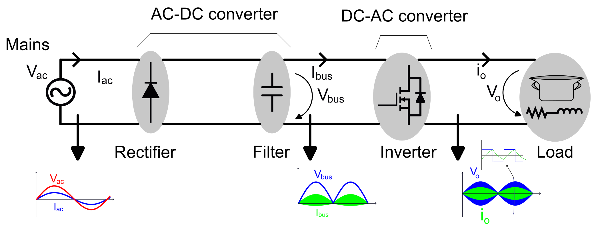
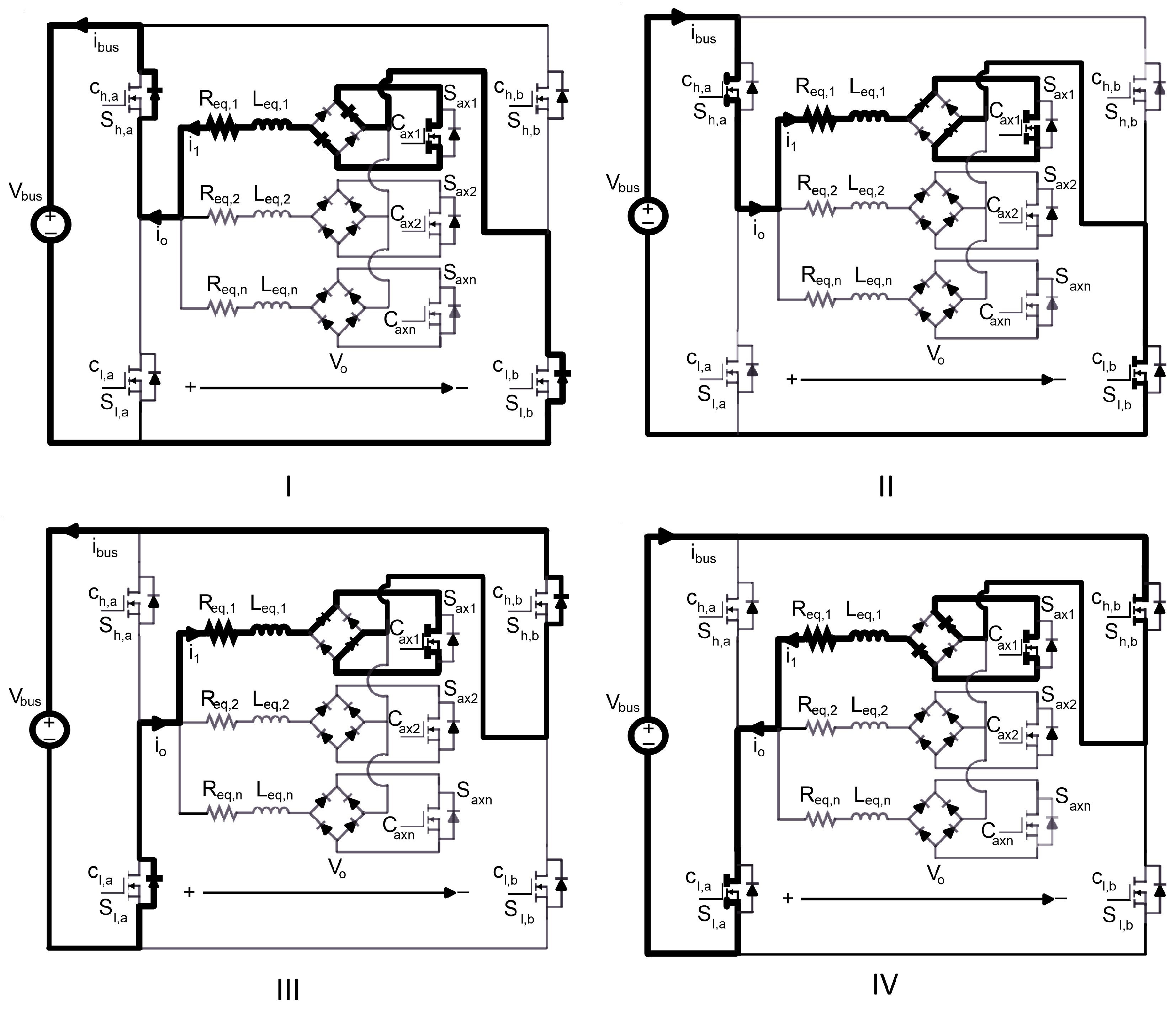
2. The Proposed Non-Resonant Full-Bridge Multi-Output Topology
2.1. Topology
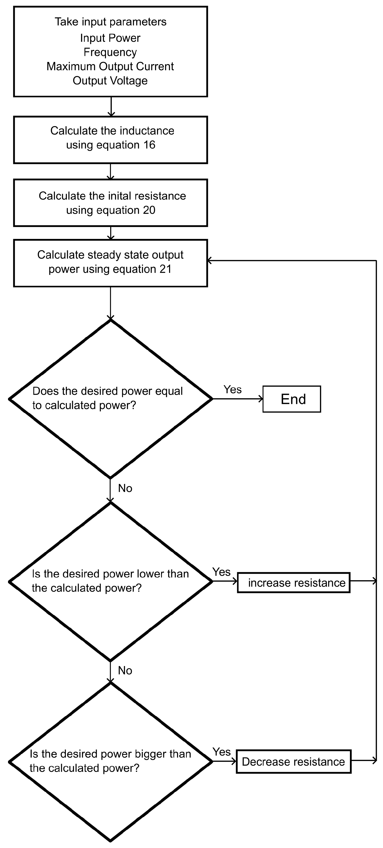
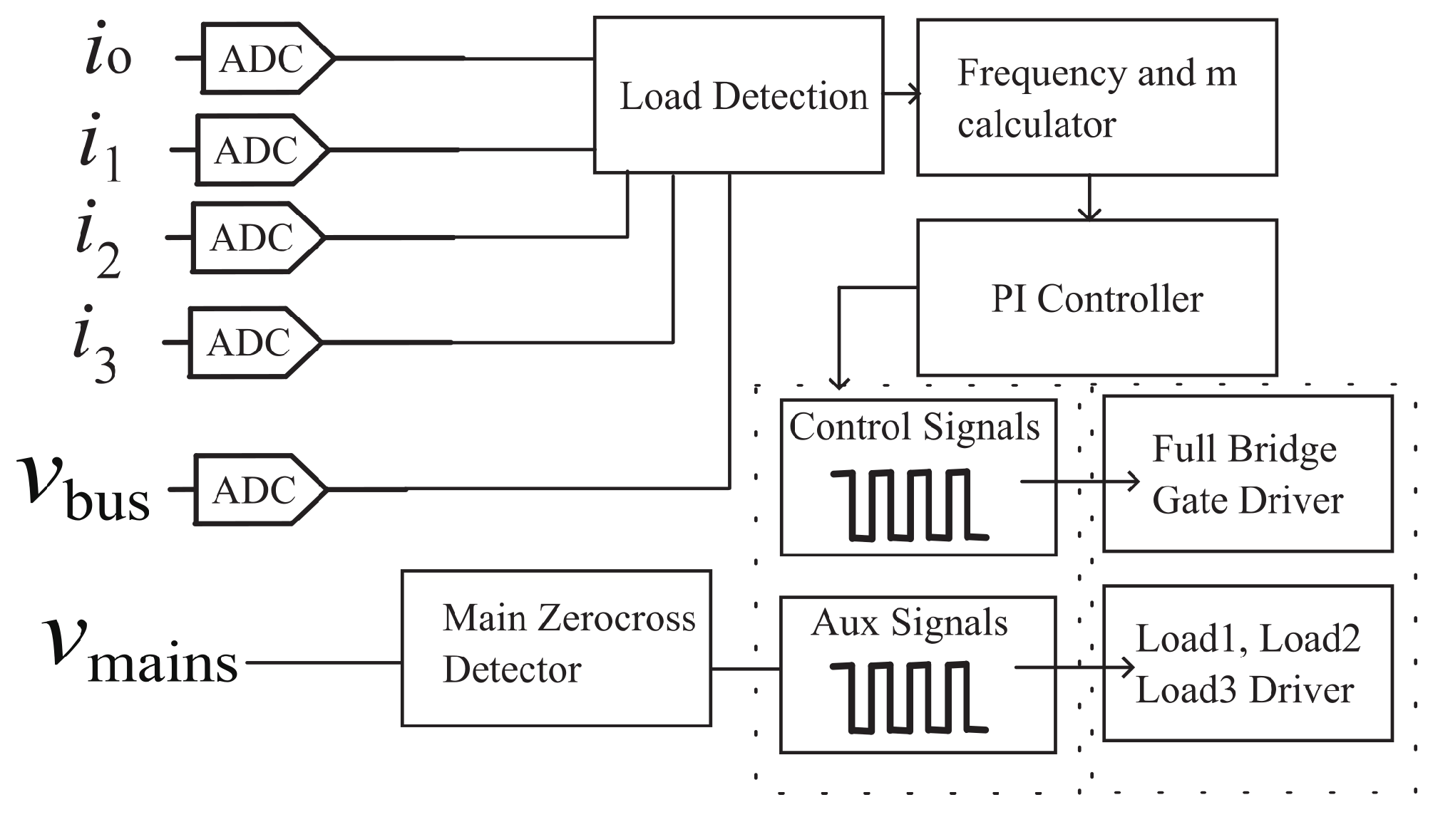
2.2. Load Sensing
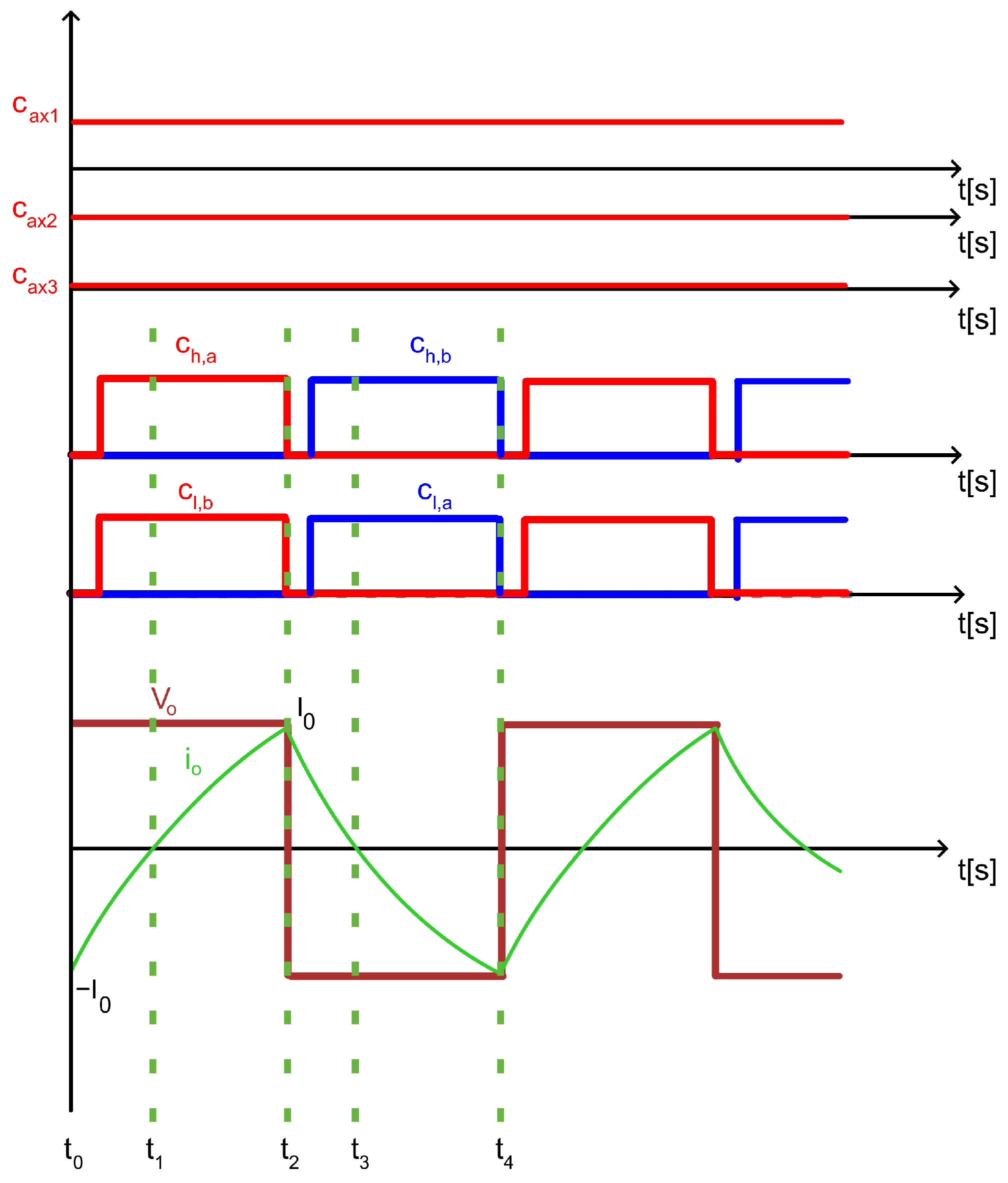
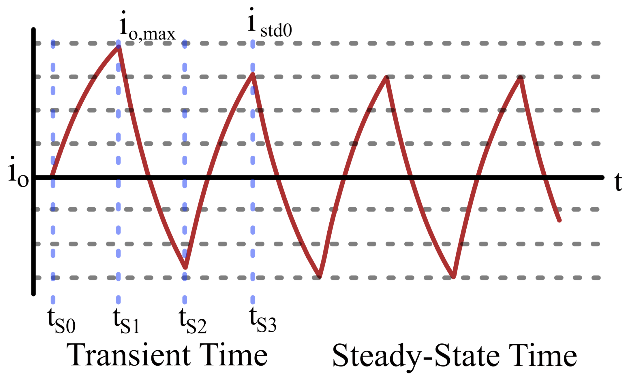
2.3. Modulation Strategies and Power Control
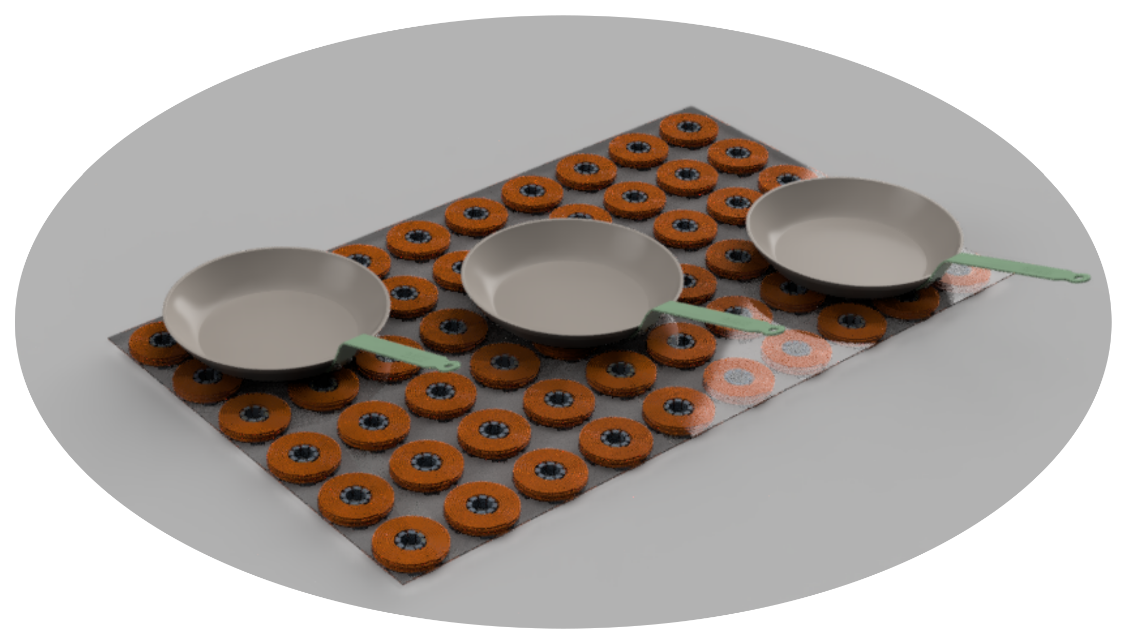
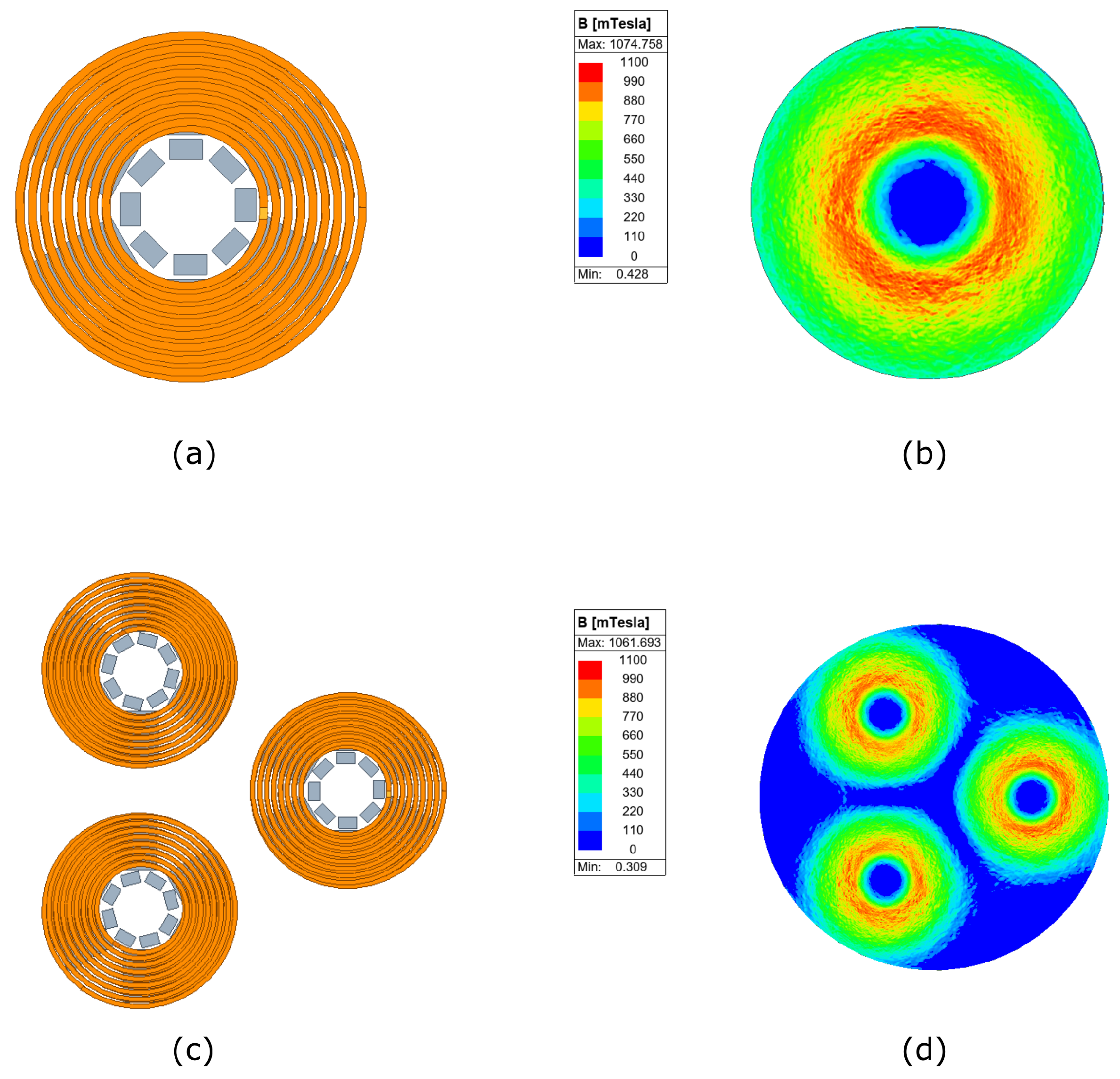
2.4. Coil Design
3. Implementation
3.1. Prototype
- A voltage rating of 1200 V and a current rating of 98 A.
- A low RDS(on) value of 19 m, ensuring minimal conduction losses and high efficiency.
- A gate threshold voltage of 4.2 V, offering immunity to parasitic turn-on events, and compatibility with a 0 V gate-off voltage.
3.2. Experimental Results and Comparison
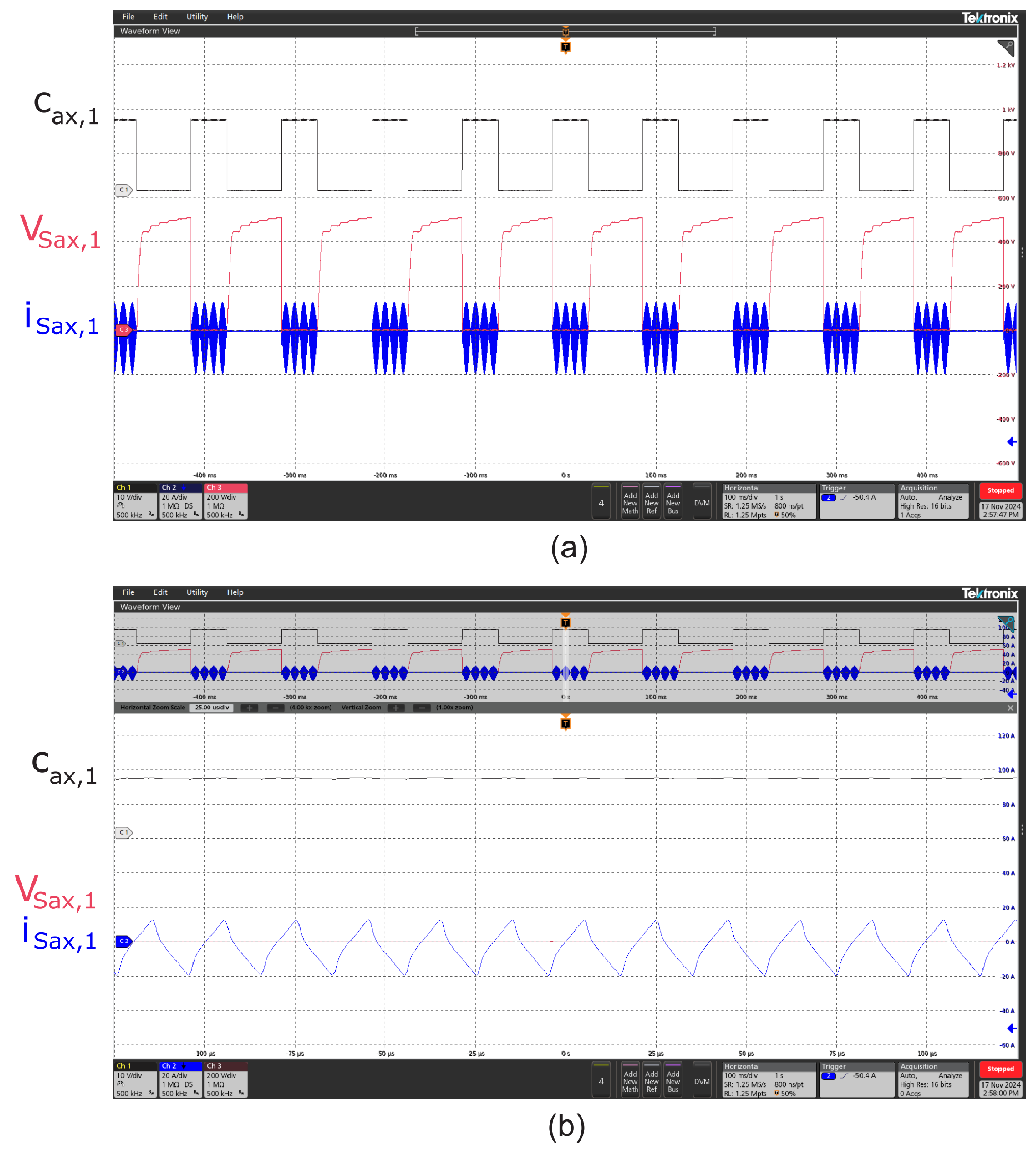
3.2.1. Control Signal and Switching Waveforms
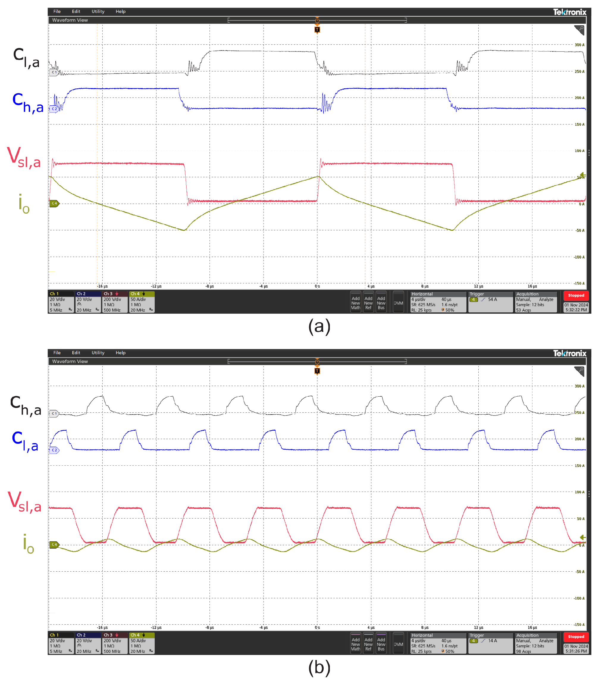
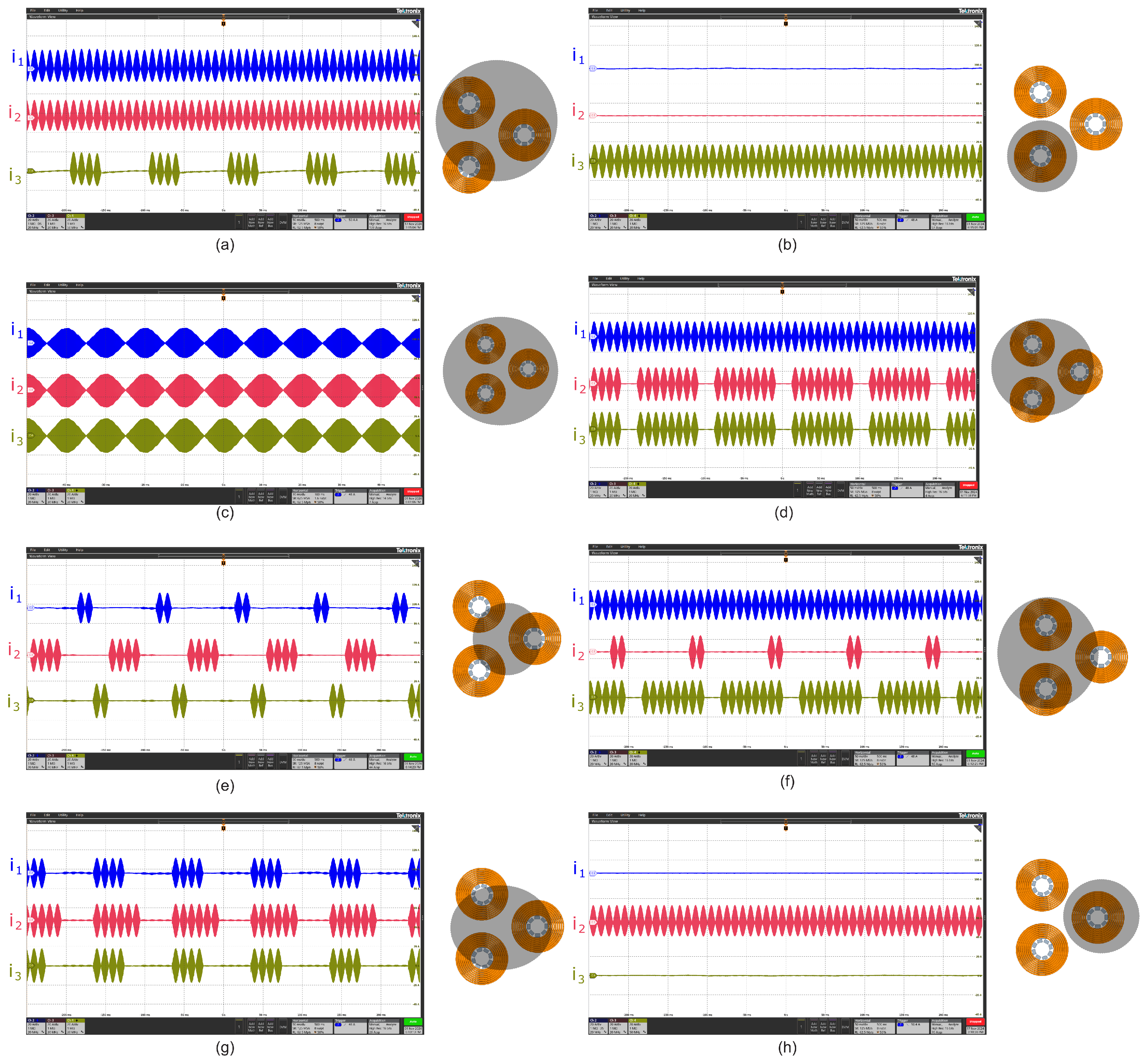
3.2.2. General Operation Waveforms
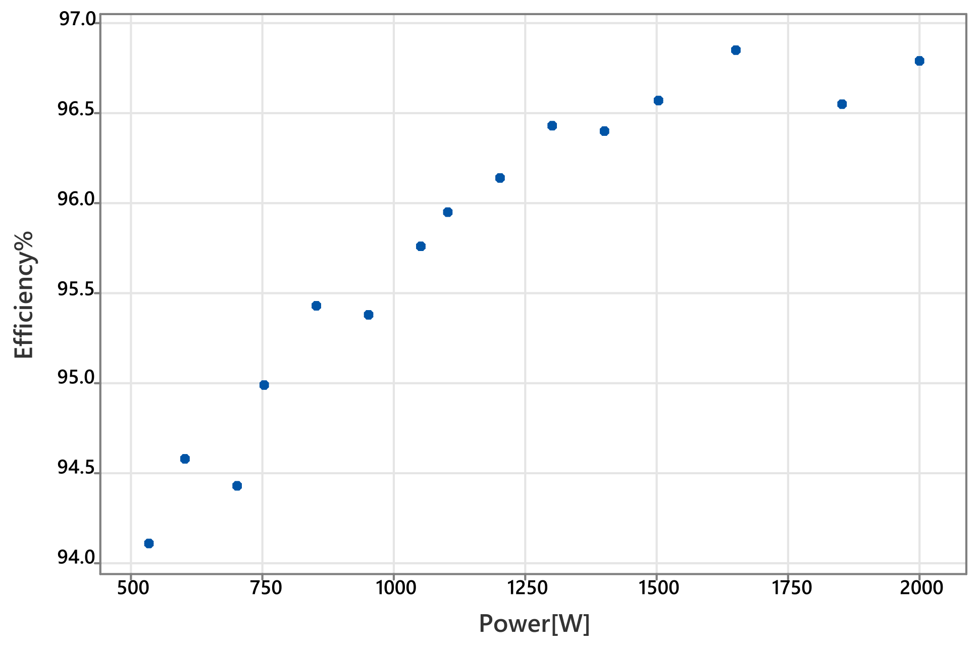
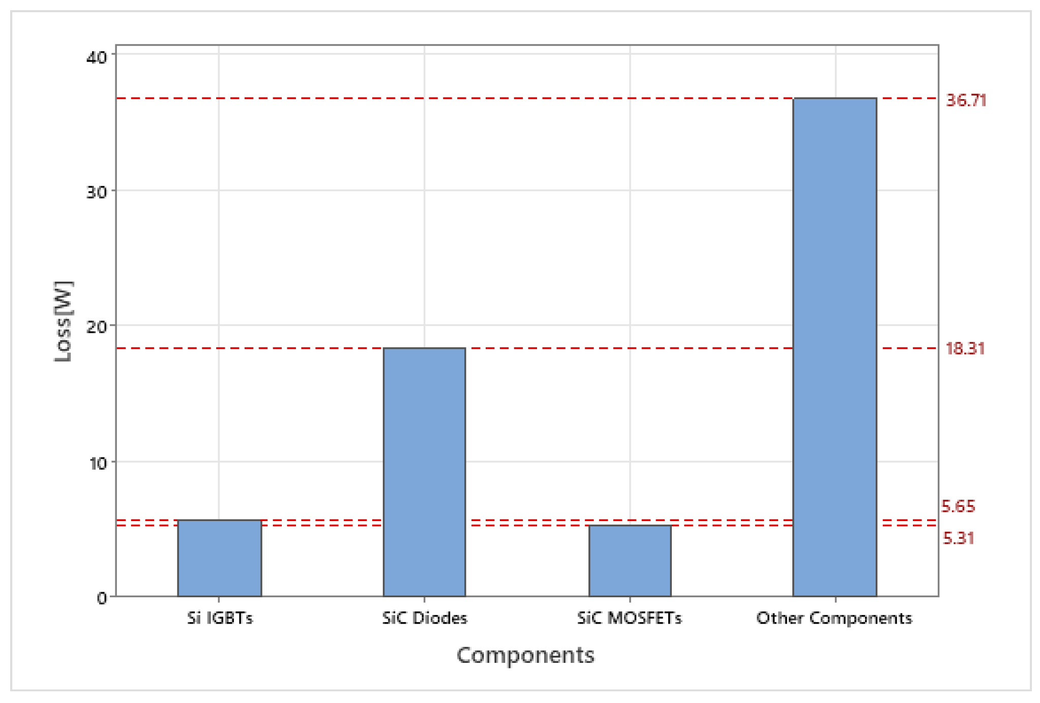
3.2.3. Efficiency Measurements Results
3.2.4. Comparison and Discussion
4. Conclusions
Author Contributions
Funding
Data Availability Statement
Acknowledgments
Conflicts of Interest
Abbreviations
| IH | Induction Heating |
| SiC | Silicon carbide |
| SSQR | Single Switch Quasi-Resonant |
| HBSR | Half-bridge series resonant |
| SE-ZCS | Single-Ended Zero-Current Switching |
| ZVS | Zero-Voltage Switching |
| QR | Quasi-Resonant |
| PDM | Pulse-density modulation |
| WBG | Wide Band Gap |
| GaN | Gallium nitride |
| PSM | Phase-shifted modulation |
| PWM | Pulse-width modulation |
| ADC | Analog to Digital Converter |
References
- Lucia, O.; Maussion, P.; Dede, E.J.; Burdio, J.M. Induction Heating Technology and Its Applications: Past Developments, Current Technology, and Future Challenges. IEEE Trans. Ind. Electron. 2014, 61, 2509–2520. [Google Scholar] [CrossRef]
- Chen, X.; Wang, J.; Ma, B.; Duan, Z.; Wang, H. Research Status and Applications of Dual-Frequency Induction Heating Power Supply. Electronics 2024, 13, 4913. [Google Scholar] [CrossRef]
- Moreland, W.C. The Induction Range: Its Performance and Its Development Problems. IEEE Trans. Ind. Appl. 1973, IA-9, 81–85. [Google Scholar] [CrossRef]
- Ozturk, M. A Simplified Design Method for Quasi-Resonant Inverter Used in Induction Hob. Electronics 2023, 12, 4145. [Google Scholar] [CrossRef]
- Altuntaş, H.; Arslan, M.S. A New Approach for Infrared Temperature Measurement Sensor Systems and Temperature Control for Domestic Induction Hobs. Sensors 2025, 25, 235. [Google Scholar] [CrossRef] [PubMed]
- Xu, Q.; Ma, F.; Luo, A.; Chen, Y.; He, Z. Hierarchical Direct Power Control of Modular Multilevel Converter for Tundish Heating. IEEE Trans. Ind. Electron. 2016, 63, 7919–7929. [Google Scholar] [CrossRef]
- Stauffer, P.R.; Cetas, T.C.; Jones, R.C. Magnetic Induction Heating of Ferromagnetic Implants for Inducing Localized Hyperthermia in Deep-Seated Tumors. IEEE Trans. Biomed. Eng. 1984, BME-31, 235–251. [Google Scholar] [CrossRef]
- Di Barba, P.; Dughiero, F.; Sieni, E. Synthesizing Distributions of Magnetic Nanoparticles for Clinical Hyperthermia. IEEE Trans. Magn. 2012, 48, 263–266. [Google Scholar] [CrossRef]
- Zungor, F.; Bodur, H.; Ozturk, M.; Obdan, H. Design Methodology of Series Resonant Half Bridge Inverter for Induction Cooker. IEEE Access 2023, 11, 135476–135492. [Google Scholar] [CrossRef]
- Ozturk, M.; Aslan, S.; Altintas, N.; Sinirlioglu, S. Comparison of Induction Cooker Power Converters. In Proceedings of the 2018 6th International Conference on Control Engineering & Information Technology (CEIT), Istanbul, Turkey, 25–27 October 2018. [Google Scholar]
- Omori, H.; Nakaoka, M. New Single-Ended Resonant Inverter Circuit and System for Induction-Heating Cooking Apparatus. Int. J. Electron. 1989, 67, 277–296. [Google Scholar] [CrossRef]
- Koertzen, H.W.; van Wyk, J.D.; Ferreira, J.A. Design of the Half-Bridge, Series Resonant Converter for Induction Cooking. In Proceedings of the PESC ’95—Power Electronics Specialist Conference, Atlanta, GA, USA, 18–22 June 1995; Volume 2, pp. 729–735. [Google Scholar]
- Pérez-Tarragona, M.; Sarnago, H.; Lucía, Ó.; Burdío, J.M. High Performance Full-Bridge Multi-Inverter Featuring 900-V SiC Devices for Domestic Induction Heating Applications. EPE J. Eur. Power Electron. Drives J. 2017, 27, 143–152. [Google Scholar] [CrossRef]
- Ngoc, H.P.; Fujita, H.; Ozaki, K.; Uchida, N. Phase Angle Control of High-Frequency Resonant Currents in a Multiple Inverter System for Zone-Control Induction Heating. IEEE Trans. Power Electron. 2011, 26, 3357–3366. [Google Scholar] [CrossRef]
- Guillen, P.; Sarnago, H.; Lucia, O.; Burdio, J.M. Multi-Output Resonant Power Converters for Domestic Induction Heating. In Proceedings of the IECON 2020 The 46th Annual Conference of the IEEE Industrial Electronics Society, Singapore, 18–21 October 2020; pp. 4320–4327. [Google Scholar]
- Sarnago, H.; Lucía, Ó.; Mediano, A.; Burdío, J.M. A Class-E Direct AC–AC Converter with Multicycle Modulation for Induction Heating Systems. IEEE Trans. Ind. Electron. 2014, 61, 2521–2530. [Google Scholar] [CrossRef]
- Hobson, L.; Tebb, D.W.; Turnbull, D. Dual-Element Induction Cooking Unit Using Power MOSFETs. Int. J. Electron. 1985, 59, 747–757. [Google Scholar] [CrossRef]
- Dawson, F.P.; Jain, P. A Comparison of Load Commutated Inverter Systems for Induction Heating and Melting Applications. IEEE Trans. Power Electron. 1991, 6, 430–441. [Google Scholar] [CrossRef]
- Pham, H.N.; Fujita, H.; Ozaki, K.; Uchida, N. Dynamic Analysis and Control for Resonant Currents in a Zone-Control Induction Heating System. IEEE Trans. Power Electron. 2013, 28, 1297–1307. [Google Scholar] [CrossRef]
- Burdío, J.M.; Monterde, F.; García, J.R.; Barragán, L.A.; Martínez, A. A Two-Output Series-Resonant Inverter for Induction-Heating Cooking Appliances. IEEE Trans. Power Electron. 2005, 20, 815–822. [Google Scholar] [CrossRef]
- Forest, F.; Laboure, E.; Costa, F.; Gaspard, J.Y. Principle of a Multi-Load/Single Converter System for Low Power Induction Heating. IEEE Trans. Power Electron. 2000, 15, 223–230. [Google Scholar] [CrossRef]
- Sarnago, H.; Saoudi, M.; Mediano, A.; Puyal, D.; Lucía, Ó. Hybrid Full/Half Wave Inverter Designed for Low Cost Induction Heating Appliances. In Proceedings of the IECON 2011—37th Annual Conference of the IEEE Industrial Electronics Society, Melbourne, Australia, 7–10 November 2011; pp. 2539–2544. [Google Scholar]
- Sarnago, H.; Lucía, Ó.; Burdío, J.M. FPGA-Based Resonant Load Identification Technique for Flexible Induction Heating Appliances. IEEE Trans. Ind. Electron. 2018, 65, 9421–9428. [Google Scholar] [CrossRef]
- Lucía, Ó.; Acero, J.; Carretero, C.; Burdío, J.M. Induction Heating Appliances: Toward More Flexible Cooking Surfaces. IEEE Ind. Electron. Mag. 2013, 7, 35–47. [Google Scholar] [CrossRef]
- Acero, J.; Burdío, J.M.; Barragán, L.A.; Navarro, D.; Alonso, R.; Ramón, J.R.; Monterde, F.; Hernández, P.; Llorente, S.; Garde, I. Domestic Induction Appliances. IEEE Ind. Appl. Mag. 2010, 16, 39–47. [Google Scholar] [CrossRef]
- Sarnago, H.; Lucía, Ó.; Pérez-Tarragona, M.; Burdío, J.M. Dual-Output Boost Resonant Full-Bridge Topology and Its Modulation Strategies for High-Performance Induction Heating Applications. IEEE Trans. Ind. Electron. 2016, 63, 3554–3561. [Google Scholar] [CrossRef]
- Sarnago, H.; Lucía, Ó.; Mediano, A.; Burdío, J.M. Design and Implementation of a High-Efficiency Multiple-Output Resonant Converter for Induction Heating Applications Featuring Wide Bandgap Devices. IEEE Trans. Power Electron. 2014, 29, 2539–2549. [Google Scholar] [CrossRef]
- Lucía, Ó.; Carretero, C.; Burdío, J.M.; Acero, J.; Almazán, F. Multiple-Output Resonant Matrix Converter for Multiple Induction Heaters. IEEE Trans. Ind. Appl. 2012, 48, 1387–1396. [Google Scholar] [CrossRef]
- Saoudi, M.; Puyal, D.; Sarnago, H.; Antón, D.; Mediano, A. A New Multiple Coils Topology for Domestic Induction Cooking System. In Proceedings of the IECON 2011—37th Annual Conference of the IEEE Industrial Electronics Society, Melbourne, Australia, 7–10 November 2011. [Google Scholar]
- Papani, S.K.; Neti, V.; Murthy, B.K. Dual Frequency Inverter Configuration for Multiple-Load Induction Cooking Application. IET Power Electron. 2015, 8, 591–601. [Google Scholar] [CrossRef]
- Khatroth, S.; Shunmugam, P. Cascaded Full-Bridge Resonant Inverter Configuration for Different Material Vessel Induction Cooking. IET Power Electron. 2020, 13, 4428–4438. [Google Scholar] [CrossRef]
- Burdío, J.M.; Barragán, L.A.; Monterde, F.; Navarro, D.; Acero, J. Asymmetrical Voltage-Cancellation Control for Full-Bridge Series Resonant Inverters. IEEE Trans. Power Electron. 2004, 19, 461–469. [Google Scholar] [CrossRef]
- Sarnago, H.; Burdío, J.M.; Lucía, Ó. High-Performance and Cost-Effective ZCS Matrix Resonant Inverter for Total Active Surface Induction Heating Appliances. IEEE Trans. Power Electron. 2019, 34, 117–125. [Google Scholar] [CrossRef]
- Sarnago, H.; Guillén, P.; Burdío, J.M.; Lucía, Ó. Multiple-Output ZVS Resonant Inverter Architecture for Flexible Induction Heating Appliances. IEEE Access 2019, 7, 157046–157056. [Google Scholar] [CrossRef]
- Ozturk, M.; Altintas, N. Multi-Output AC–AC Converter for Domestic Induction Heating. Electr. Eng. 2023, 105, 297–316. [Google Scholar] [CrossRef]
- Rehm, F.; Hiller, M. A Non-Resonant Multi-Output Half-Bridge Inverter for Flexible Cooking Surfaces. In Proceedings of the 2023 11th International Conference on Power Electronics and ECCE Asia (ICPE 2023—ECCE Asia), Jeju Island, Republic of Korea, 22–25 May 2023; pp. 2591–2597. [Google Scholar]
- Raeber, M.; Amiras, P.; Heinzelmann, A. Analysis on the Use of Non-Resonant Inverters in Single-Phase Induction Heating Applications. In Proceedings of the IECON 2020 The 46th Annual Conference of the IEEE Industrial Electronics Society, Singapore, 18–21 October 2020; pp. 4315–4319. [Google Scholar]
- Jordan, J.; Esteve, V.; Sanchis-Kilders, E.; Dede, E.J.; Maset, E.; Ejea, J.B.; Ferreres, A. A Comparative Performance Study of a 1200 V Si and SiC MOSFET Intrinsic Diode on an Induction Heating Inverter. IEEE Trans. Power Electron. 2014, 29, 2550–2562. [Google Scholar] [CrossRef]
- Aslan, S.; Ozturk, M.; Altintas, N. A Comparative Study of SiC and Si Power Devices in Induction Cookers. In Proceedings of the 2018 5th International Conference on Electrical and Electronic Engineering (ICEEE), Istanbul, Turkey, 3–5 May 2018; pp. 297–301. [Google Scholar]
- Sarnago, H.; Burdío, J.M.; Lucía, Ó. High-Frequency GaN-Based Induction Heating Versatile Module for Flexible Cooking Surfaces. In Proceedings of the 2019 IEEE Applied Power Electronics Conference and Exposition (APEC), Anaheim, CA, USA, 17–21 March 2019; pp. 448–452. [Google Scholar]
- Jang, E.; Kwon, M.J.; Park, S.M.; Ahn, H.M.; Lee, B.K. Analysis and Design of Flexible-Surface Induction-Heating Cooktop with GaN-HEMT-Based Multiple Inverter System. IEEE Trans. Power Electron. 2022, 37, 12865–12876. [Google Scholar] [CrossRef]
- Erken, A.; Obdan, A.H. Examining the Optimal Use of WBG Devices in Induction Cookers. Appl. Sci. 2023, 13, 12517. [Google Scholar] [CrossRef]
- Lucía, Ó.; Burdío, J.M.; Millan, I.; Acero, J.; Puyal, D. Load-Adaptive Control Algorithm of Half-Bridge Series Resonant Inverter for Domestic Induction Heating. IEEE Trans. Ind. Electron. 2009, 56, 3106–3116. [Google Scholar] [CrossRef]


| Parameters | Input Parameters’ Explanation | Value |
|---|---|---|
| P | Power | 670 W × 3 (2010 W) |
| F | Frequency | 50 kHz |
| Maximum output current | 33.24 A | |
| Output voltage | 226 V |
| Parameters and Aspects | Single Coil Details | Triple Coil Details |
|---|---|---|
| Parameter determination (Resistance (R), Inductance (L)) | R = 8 , L = 68 μH Power = 670 W. | Parameters for individual coils remain the same; total power = 2010 W |
| Operating conditions | Power = 670 W Current = 18 A Frequency = 50 kHz. | Total power = 2010 W Total current = 54 A Frequency = 50 kHz |
| Coil current and frequency | Sinusoidal current of 18 A peak, 50 kHz. | Sinusoidal current distributed across three coils (54 A total) |
| Analysis convergence | Mesh density = 1.72%. | Mesh density = 1.72% |
| Boundary conditions | Vacuum environment; domain size large enough to avoid flux distortion. | Same as single coil |
| Current excitation | Direct sinusoidal current applied (18 A, 50 kHz). | Total sinusoidal current distributed across coils (54 A, 50 kHz) |
| Topology | Transistor | Relay | Diode |
|---|---|---|---|
| Non-resonant multi-output half-bridge inverter [36] | 2 | 0 | |
| Full-bridge series resonant multi-inverter [13] | 0 | 0 | |
| Proposed topology | 0 | 4 |
| Topology | Control | Output Power | Switching Frequency |
|---|---|---|---|
| Non-resonant multi-output half-bridge inverter | PSM, FM | 828 W | 100–500 kHz |
| Full-bridge series resonant multi-inverter | PSM, PDM, FM | 700 W | 146–240 kHz |
| Proposed topology | PDM, FM | 2010 W | 50–190 kHz |
Disclaimer/Publisher’s Note: The statements, opinions and data contained in all publications are solely those of the individual author(s) and contributor(s) and not of MDPI and/or the editor(s). MDPI and/or the editor(s) disclaim responsibility for any injury to people or property resulting from any ideas, methods, instructions or products referred to in the content. |
© 2025 by the authors. Licensee MDPI, Basel, Switzerland. This article is an open access article distributed under the terms and conditions of the Creative Commons Attribution (CC BY) license (https://creativecommons.org/licenses/by/4.0/).
Share and Cite
Aslan, S.; Oktay, U.; Altintas, N. A Novel Non-Resonant Full-Bridge Multi-Output Topology for Domestic Induction Heating Applications. Electronics 2025, 14, 596. https://doi.org/10.3390/electronics14030596
Aslan S, Oktay U, Altintas N. A Novel Non-Resonant Full-Bridge Multi-Output Topology for Domestic Induction Heating Applications. Electronics. 2025; 14(3):596. https://doi.org/10.3390/electronics14030596
Chicago/Turabian StyleAslan, Sezer, Ulas Oktay, and Nihan Altintas. 2025. "A Novel Non-Resonant Full-Bridge Multi-Output Topology for Domestic Induction Heating Applications" Electronics 14, no. 3: 596. https://doi.org/10.3390/electronics14030596
APA StyleAslan, S., Oktay, U., & Altintas, N. (2025). A Novel Non-Resonant Full-Bridge Multi-Output Topology for Domestic Induction Heating Applications. Electronics, 14(3), 596. https://doi.org/10.3390/electronics14030596