Article

A 5-Transistor CMOS Voltage Reference with Double Supply-Regulation

1
Department of Electronic Engineering, Hanbat National University, Daejeon 34158, Republic of Korea
2
School of Electronic Engineering, Engineering Research Institute (ERI), Gyeongsang National University, Jinju 52828, Republic of Korea
*
Author to whom correspondence should be addressed.
Electronics 2025, 14(3), 588; https://doi.org/10.3390/electronics14030588
Submission received: 20 December 2024 / Revised: 17 January 2025 / Accepted: 26 January 2025 / Published: 1 February 2025
(This article belongs to the Special Issue New Horizons and Recent Advances of Power Electronics)

Abstract

:
This paper presents an ultra-low-power CMOS voltage reference designed and verified in an 180 nm standard CMOS technology. To achieve DC and AC supply sensitivity under 0.01%/V and −100 dB, it employs a single transistor and two 2-T cores to improve supply immunity with minimal overhead, adding only one drain-to-source voltage for the total supply voltage. The proposed design achieves a line sensitivity of 0.0027%/V in a supply voltage range of 0.5 V to 2 V and consumes 630 pW with a supply voltage of 0.5 V. The simulated temperature coefficient is 12 ppm/°C in a temperature range of −40 °C to 150 °C, and the simulated power supply rejection ratio is −100.5 dB at 100 Hz without requiring any output decoupling capacitor.

1. Introduction

The rapid advancement of sensor technology has enabled various applications, including the Internet of Things (IoT) nodes and portable electronics. However, these applications often operate in energy-constrained environments where power availability is limited, requiring ultra-low-power operation. Voltage references, as essential building blocks for generating internal biases, must maintain accurate and stable outputs while consuming minimal power to extend system longevity. In addition to low power, such systems require voltage sources with low supply voltage dependency, as the supply voltage can fluctuate significantly due to power/data transfer activities, energy harvesting variations, or external interferences.
Voltage reference can be categorized into three types: bandgap reference (BGR) [1,2], hybrid reference (HR) [3,4], and CMOS reference (CR) [5,6,7,8,9,10,11,12]. In BGR and HR circuits, the reference voltage is generated by adding a proportional-to-absolute-temperature (PTAT) voltage to a complementary-to-absolute-temperature (CTAT) voltage of a BJT, effectively canceling out temperature variation. While BGR and HR topologies offer strong immunity to process, voltage, and temperature (PVT) variations, their reliance on BJTs limits their adoption in supply voltage-constrained environments.
As an alternative, CRs address this limitation by operating the transistor in the subthreshold region and exploiting the threshold voltages as a reference instead of the silicon bandgap voltage. Ref. [5] presents a 2-transistor (2-T)-based voltage reference that generates a reference voltage based on the threshold difference of two different transistor types. This approach achieves power consumption under nanowatt-level while maintaining the conventional requirement such as temperature coefficient (TC) and minimum supply voltage.
However, dc and ac supply stability, determined by the intrinsic gain of the transistors, may deteriorate when the reference voltage is scaled up [6] or when the circuit is implemented in recent technology nodes [7].
Various methods have been proposed to suppress the supply dependency [8,9,10,11]. Ref. [8] employed a low-impedance diode-connected transistor to mitigate the impact of the supply voltage on the reference core, albeit at the cost of significantly higher power consumption compared to 2-T reference. Refs. [9,10] proposed a current subtraction path to compensate for supply dependency, requiring trimming or output decoupling capacitor. Ref. [11] duplicated three 2-T cores to regulate the effective supply voltage, though its power supply rejection ratio (PSRR) remains unverified. Ref. [12] proposed a gate-leakage-based TC compensation and a diode-connected voltage divider to alleviate the temperature dependence, but this approach introduces increased costs for trimming options.
This paper presents an ultra-low-power CMOS voltage reference that utilizes a single transistor and two 2-T cores to enhance the supply immunity with minimal overhead, requiring only the additional drain-to-source voltage for the overall supply voltage. The overall circuit, implemented using a total of five transistors (5-T), is designed and verified in a 180 nm standard CMOS technology. The proposed circuit consumes 630 pW at a supply voltage of 0.5 V, achieving a line sensitivity (LS) of 0.0027%/V across a supply voltage range of 0.5 V to 2 V and a PSRR of −100.5 dB at 100 Hz without requiring any decoupling capacitor. The TC of the proposed circuit is 12 ppm/°C over a temperature range of −40 °C to 150 °C.
The remainder of this paper is organized as follows: Section 2 describes the proposed double regulation method and compares it with the conventional 2-T CR. Section 3 presents the simulation results, demonstrating the performance improvements. Finally, Section 4 concludes the paper.

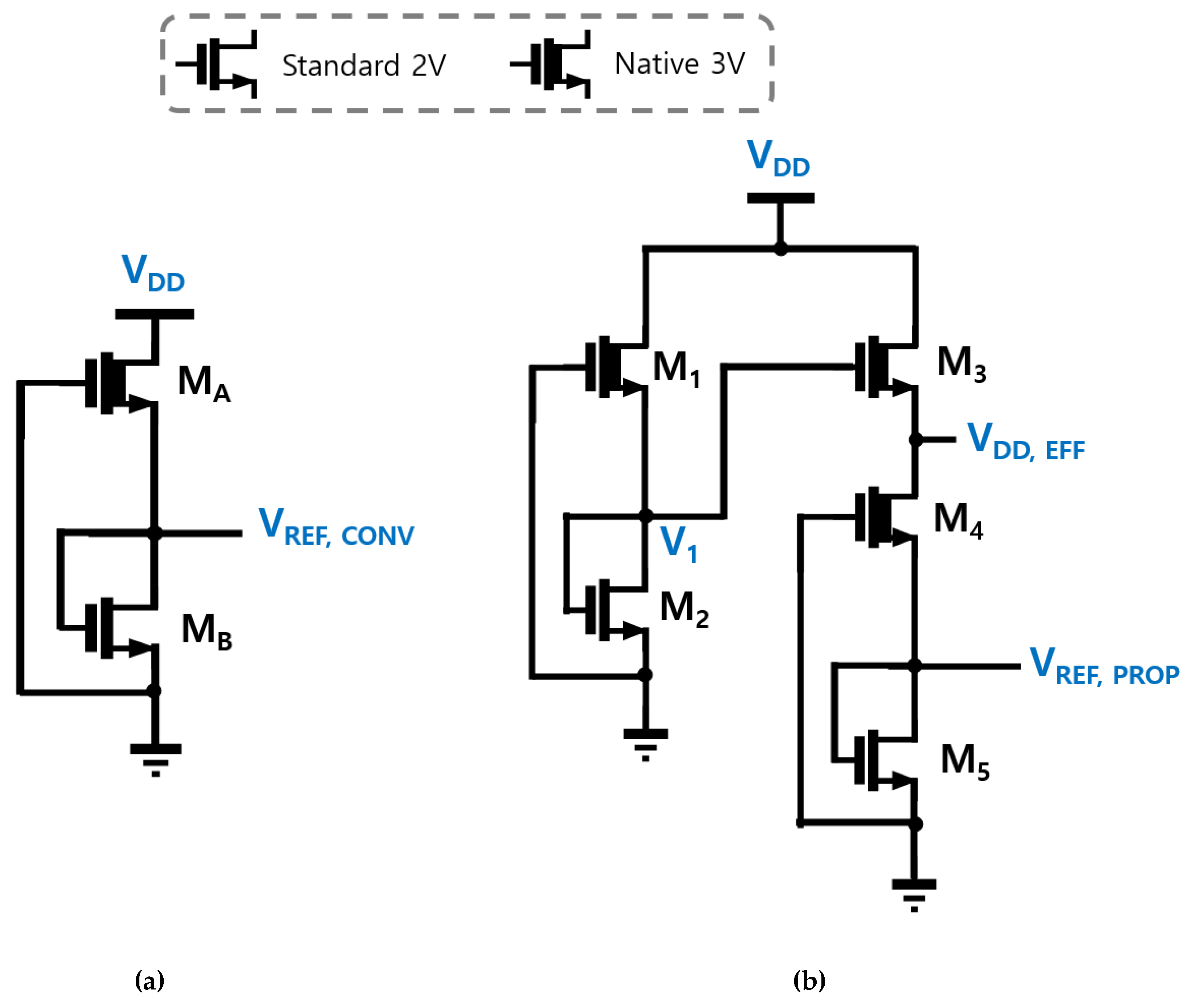
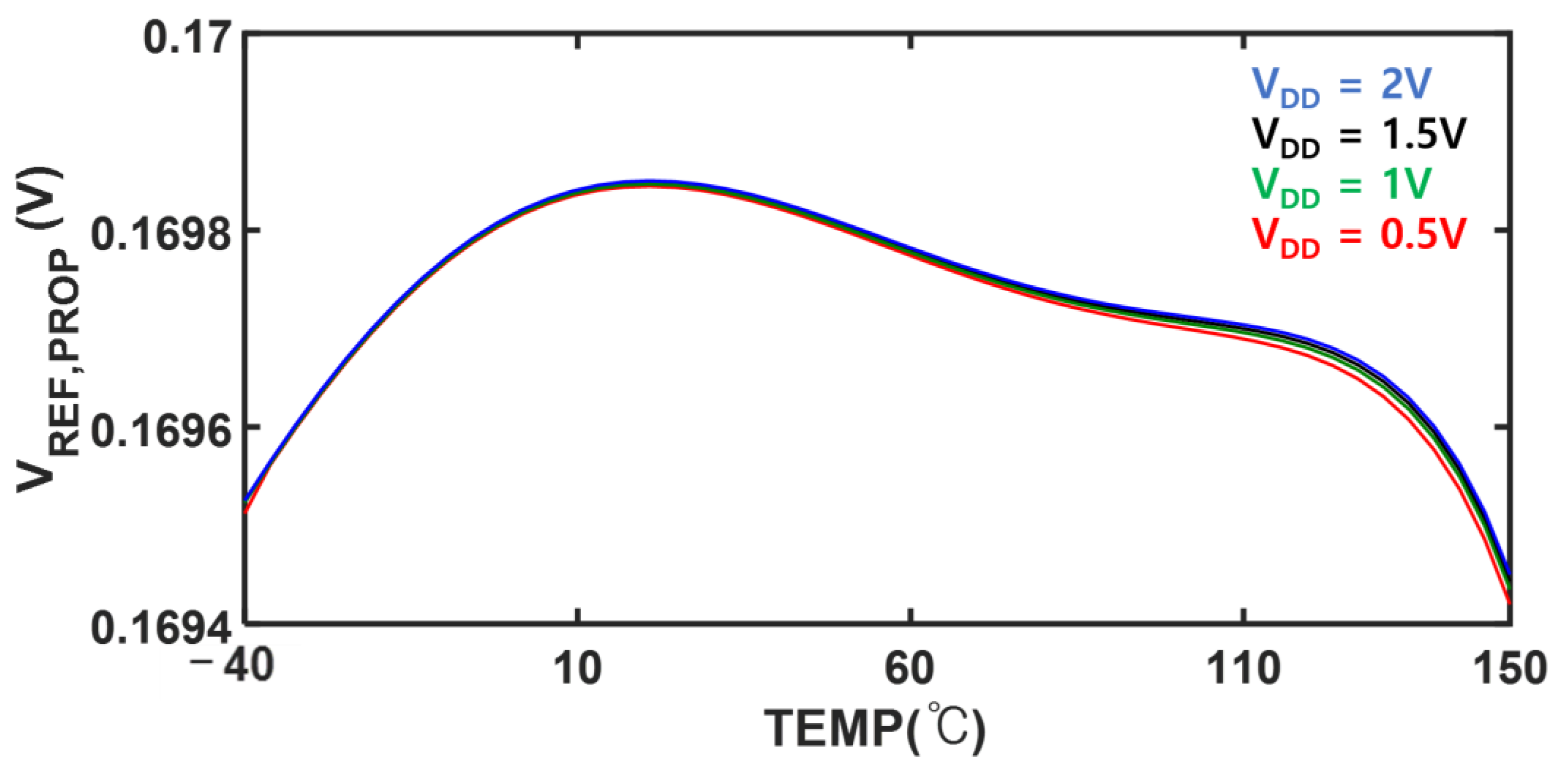
2. Proposed CR with Double Supply Regulation and Post-Layout Simulation Results on Supply Variations

Figure 1 illustrates the overall circuit diagrams of the conventional 2-T CR [5] and the proposed 5-T CR. By equating the subthreshold current equations of two transistors in Figure 1a, the reference voltage of the conventional 2-T CR, VREF,CONV, can be expressed as
V R E F , C O N V = V T H , B V T H , A + m B V T ln W A L B W B L A ,
where the subscripts A and B represent the parameters of MA and MB, respectively, and VTH, VT, and m denote the threshold voltage, thermal voltage, and subthreshold slope factor. In Equation (1), parameters such as mobility, oxide capacitance, and subthreshold slope factor are assumed to be identical for both transistors to simplify the equation. The optimum dimension ratio between MA and MB can be derived using the following equation [5]:
W B L A W A L B e C T H , B C T H , A T m B V T ,
where C represents the first-order temperature dependency of the threshold voltage.
The proposed 5-T CR is depicted in Figure 1b. Based on the conventional 2-T core (M1 and M2), the first-regulated output, V1, is used to provide an effective supply voltage for the second-2T core, VDD,EFF, via a single transistor (M3) operating as a source follower. This output is then further regulated by another 2-T core (M4 and M5) to generate the final reference voltage, VREF,PROP. It is worth noting that the core operation of the proposed 5-T CR remains identical to that of the conventional 2-T CR, except for the double regulation process. Consequently, Equations (1) and (2) from the conventional 2-T CR can also be applied to the proposed design. In the proposed circuit, nominal transistors are used for M2 and M5, while native transistors are used for M1, M3, and M4. Each body of the transistors is connected to the ground. The dimensions of all transistors are listed in Table 1.
Figure 2 shows the small-signal models of the conventional 2-T CR (Figure 2a) and the proposed 5-T CR (Figure 2b), where gm and ro are the transconductance and output resistance of the transistors, respectively, with subscripts corresponding to individual transistors. Using Kirchhoff’s Law in Figure 2a, the supply sensitivity of the 2-T CR can be derived as follows:
V R E F , C O N V V D D   1 g m , A + g m , B r o , A + 1     .
A similar approach can be applied to derive the equations for the proposed 5-T CR. The regulated voltage, VDD,EFF, can be expressed as
V D D , E F F g m , 3 V R E F , C O N V + V D D r o , 3 + g m , 4 V R E F , P R O P + V R E F , P R O P r o , 4 g m , 3 r o , 3 r o , 4 + r o , 4 + r o , 3 r o , 3 r o , 4   .
By substituting V R E F , C O N V from Equation (3) into Equation (4) and changing the subscripts A and B to 1 and 2, VDD,EFF can be rearranged as
V D D , E F F = g m , 3 V D D   g m , 1 r o , 1 + g m , 2 r o , 1 + 1 + V D D r o , 3 + g m , 4 V R E F , P R O P + V R E F , P R O P r o , 4 × r o , 3 r o , 4 g m , 3 r o , 3 r o , 4 + r o , 4 + r o , 3 .
Additionally, the relationship between M4 and M5 can be written as
V R E F , P R O P = 1 r o , 4 V D D ,   E F F g m , 4 + g m , 5 + 1 r o , 4 .
Substituting V D D , E F F from Equation (5) into Equation (6), the final reference voltage, VREF,PROP, can be derived as
V R E F ,   P R O P V D D =   g m , 1 + g m , 2 r o , 1 + g m , 3 r o , 3 g m , 3 ( g m , 1 + g m , 2 ) ( g m , 4 + g m , 5 ) r o , 1 r o , 3 r o , 4 .
Assuming gm,1 = gm,a, gm,2 = gm,b, and ro,1 = ro,a, the supply stability ratio between the conventional 2-T and the proposed 5-T can be derived from Equations (3) and (7) as follows:
V R E F , C O N V / V D D V R E F ,   P R O P / V D D = 1 ( g m , 1 + g m , 2 ) r o , 1 /   g m , 1 + g m , 2 r o , 1 + g m , 3 r o , 3 g m , 3 g m , 1 + g m , 2 ) ( g m , 4 + g m , 5 r o , 1 r o , 3 r o , 4 = g m , 3 g m , 4 + g m , 5 r o , 1 r o , 3 r o , 4   g m , 1 + g m , 2 r o , 1 + g m , 3 r o , 3 .
Consequently, the supply sensitivity of the proposed 5-T CR is improved by approximately one order of magnitude, proportional to the intrinsic gain of a transistor (gmro). In our design, the value calculated from Equation (8) is 85.8, which may vary depending on the transistor dimensions or level of flowing currents. The device parameters for each transistor in the proposed 5-T CR are listed in Table 2. Since M3 functions as a source follower and does not affect the core regulation process, its dimension is designed to be minimum to reduce the area cost.
Figure 3 compares the original supply voltage, VDD, with the effective supply voltage, VDD,EFF, after passing through the first 2-T core and M3. Since the regulated supply is applied to the 2-T core, the proposed 5-T CR demonstrates superior LS compared to the conventional 2-T core. This improvement is quantified as gmro, as shown in Figure 4. The simulated LS of the proposed 5-T CR is 0.0027%/V across a supply voltage range of 0.5 V to 2 V, greatly outperforming the conventional 2-T CR, which exhibits a LS of 0.304%/V over the same range.
The minimum supply voltage condition for the 2-T CR in Figure 1a can be written as
V D D , m i n , C O N V = V R E F + V D S , A ,
whereas the minimum supply voltage for the proposed 5-T CR in Figure 1b is derived as
V D D , m i n , P R O P = V R E F + V D S , 3 + V D S , 4 = V D D , m i n , C O N V + V D S .
For fair comparison, both designs were configured to dissipate the same amount of current per each branch. While the proposed 5-T CR consumes twice the current and requires a supply headroom of VDS, LS achieves about 50 times better and PSRR achieves about 30 times better supply characteristics.

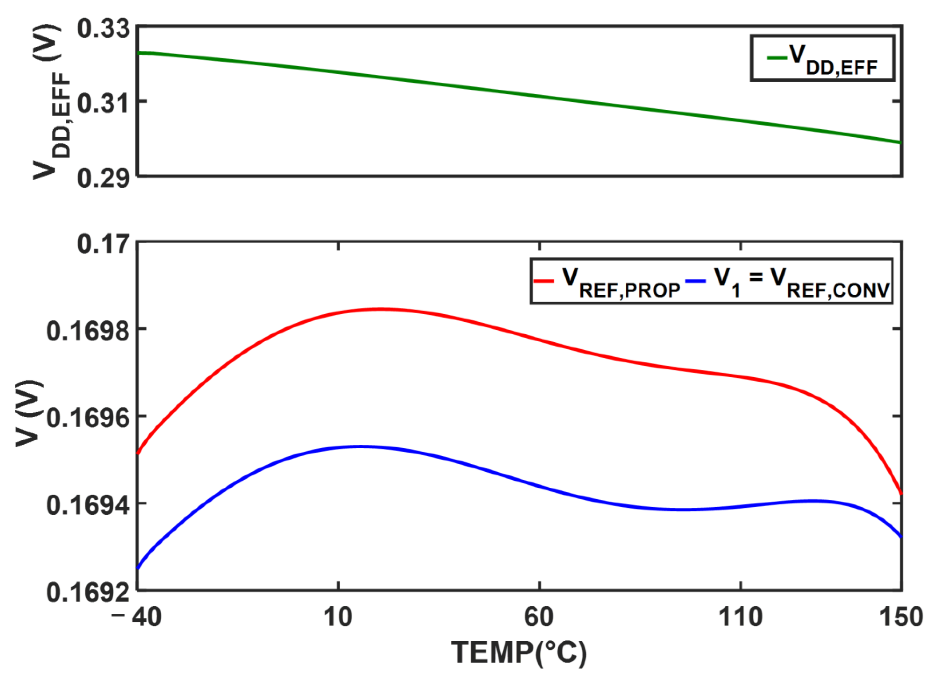
3. Post-Layout Simulation Results on Process and Temperature Variations

Figure 5 shows the simulated PSRR for each node voltage over a frequency range from 1 Hz to 100 MHz. By applying the pre-regulated voltage, VDD,EFF, instead of the overall supply voltage, VDD, to the 2-T core, the proposed 5-T CR achieves double regulation. The final reference voltage, VREF,PROP, shows a PSRR of −100.5 dB at 100 Hz, which is an improvement of approximately −40 dB compared to the conventional 2-T CR. The dominant pole remains at the same frequency as that of the conventional 2-T CR.
Figure 6 illustrates temperature dependency of each node voltage. Through the modulated threshold voltage of the native transistor, M3, the supply voltage, VDD,EFF, for the 2-T core is successfully generated from the first regulated voltage, V1. The TC of VREF,PROP is 12 ppm/ ° C over a temperature range from −40 °C to 150 °C. Despite the significant suppression of the achieved supply variation, there is no penalty in temperature characteristics. Figure 7 shows the simulated temperature dependency of VREF,PROP at different supply voltage levels. Thanks to the superior supply immunity, the overall shape and TC remain regardless of the supply voltage level.
To verify the inaccuracy of VREF,PROP across multiple samples, a Monte Carlo simulation with 500 samples is performed, accounting for process, mismatch, and both (process and mismatch) variations, respectively. Figure 8a shows the distribution of VREF,PROP, revealing an average of 184.9 mV and a standard deviation of 11.6 mV. Since VREF,PROP is a function of threshold difference of two types of transistors, the main source for variation is the process variation. Figure 8b presents the statistical spread for TC, showing an average of 14.4 ppm/°C and a standard deviation of 6.1 ppm/°C. The worst-case and the best-case TCs are 30.9 ppm/°C and 4.33 ppm/°C, respectively. Figure 8c depicts the LS distribution at room temperature, showing an average of 0.00382%/V and a standard deviation of 0.0011%/mV. The worst-case and the best-case LS values are 0.0022%/V and 0.0075%/V, respectively. Figure 9 demonstrates an exemplary layout of the proposed 5-T CR, with an active area of 787.3 µm2 (18.7 µm × 42.1 µm).
Table 3 summarizes and compares the performance of the proposed 5-T CR with recently reported voltage references. Figure 10 compares the performances of the previously reported CRs and the proposed CR by visualizing the TC against the maximum operating temperature and the LS against the minimum supply voltage.

4. Conclusions

This paper presented a CR optimized for ultra-low-power applications, with improvements in LS and PSRR achieved using only five transistors, without any penalty in TC. The circuit was designed and verified in an 180 nm standard CMOS technology, generating a reference voltage of 169 mV and consuming only 630 pW under nominal conditions. It achieves an average TC of 12 ppm/°C over a temperature range of −40 °C to 150 °C and an average LS of 0.0027%/V across a supply voltage range of 0.5 V to 2 V at room temperature. The simulated PSRR is −100.5 dB at the 100 Hz and at a minimum operating supply voltage of 0.5 V. The proposed CR is suitable for energy-constrained electronics such as IoT systems, where accuracy against PVT variations and ultra-low power operation is critical.

Author Contributions

Conceptualization, M.J. and Y.J.; methodology, M.J. and Y.J.; software, M.J. and K.M.; validation, M.J., K.M., H.S. and Y.J.; formal analysis, M.J., H.S. and Y.J.; investigation, M.J. and Y.J.; resources, Y.J.; data curation, M.J.; writing—original draft preparation, M.J.; writing—review and editing, H.S. and Y.J.; visualization, M.J.; supervision, Y.J.; project administration, Y.J. All authors have read and agreed to the published version of the manuscript.

Funding

This results was supported by “Regional Innovation Strategy (RIS)” through the National Research Foundation of Korea (NRF) funded by the Ministry of Education (MOE) (2021RIS-004). This research was supported by the MSIT (Ministry of Science and ICT), Korea, under the ICAN (ICT Challenge and Advanced Network of HRD) support program (IITP-2025-RS-2022-00156212) supervised by the IITP (Institute for Information & Communications Technology Planning & Evaluation).

Data Availability Statement

The original contributions presented in this study are included in the article. Further inquiries can be directed to the corresponding author(s).

Conflicts of Interest

The authors declare no conflicts of interest.

References

  1. Chen, K.; Petruzzi, L.; Hulfachor, R.; Onabajo, M. A 1.16-V 5.8-to-13.5-ppm/°C Curvature-Compensated CMOS Bandgap Reference Circuit with a Shared Offset-Cancellation Method for Internal Amplifiers. IEEE J. Solid-State Circuits 2021, 56, 267–276. [Google Scholar] [CrossRef]
  2. Kim, M.; Cho, S. A Single BJT Bandgap Reference with Frequency Compensation Exploiting Mirror Pole. IEEE J. Solid-State Circuits 2021, 56, 2902–2912. [Google Scholar] [CrossRef]
  3. Ji, Y.; Lee, J.; Kim, B.; Park, H.J.; Sim, J.Y. A 192-pW Voltage Reference Generating Bandgap-Vth with Process and Temperature Dependence Compensation. IEEE J. Solid-State Circuits 2019, 54, 3281–3291. [Google Scholar] [CrossRef]
  4. Lee, I.; Blaauw, D. A 31 pW-to-113 nW Hybrid BJT and CMOS Voltage Reference with 3.6% ±3σ-inaccuracy from 0 °C to 170 °C for Low-Power High-Temperature IoT Systems. In Proceedings of the Symposium on VLSI Circuits, Kyoto, Japan, 9–14 June 2019; pp. C142–C143. [Google Scholar] [CrossRef]
  5. Seok, M.; Kim, G.; Blaauw, D.; Sylvester, D. A Portable 2-Transistor Picowatt Temperature-Compensated Voltage Reference Operating at 0.5 V. IEEE J. Solid-State Circuits 2012, 47, 2534–2545. [Google Scholar] [CrossRef]
  6. Lee, I.; Sylvester, D.; Blaauw, D. A Subthreshold Voltage Reference with Scalable Output Voltage for Low-Power IoT Systems. IEEE J Solid-State Circuits 2017, 52, 1443–1449. [Google Scholar] [CrossRef]
  7. Huang, C.J.; Lai, Y.J.; Yang, Y.J.O.; Chen, H.W.; Kuo, C.C.; Chen, K.H.; Lin, Y.H.; Lin, S.R.; Tsai, T.Y. A 4.2 nW and 18 ppm/°C Temperature Coefficient Leakage-Based Square Root Compensation (LSRC) CMOS Voltage Reference. IEEE Trans. Circuits Syst. II Express Briefs 2019, 66, 728–732. [Google Scholar] [CrossRef]
  8. Lin, J.; Wang, L.; Zhan, C.; Lu, Y. A 1-nW Ultra-Low Voltage Subthreshold CMOS Voltage Reference with 0.0154%/V Line Sensitivity. IEEE Trans. Circuits Syst. II Express Briefs 2019, 66, 1653–1657. [Google Scholar] [CrossRef]
  9. Wang, Y.; Sun, Q.; Luo, H.; Wang, X.; Zhang, R.; Zhang, H. A 48 pW, 0.34 V, 0.019%/V Line Sensitivity Self-Biased Subthreshold Voltage Reference with DIBL Effect Compensation. IEEE Trans. Circuits Syst. I Regul. Pap. 2020, 67, 611–621. [Google Scholar] [CrossRef]
  10. Azimi, M.; Habibi, M.; Crovetti, P. A Two-Stage Sub-Threshold Voltage Reference Generator Using Body Bias Curvature Compensation for Improved Temperature Coefficient. Electronics 2024, 13, 1390. [Google Scholar] [CrossRef]
  11. Bialek, H.; Johnston, M.L.; Natarajan, A. A 6-Transistor Ultra-Low Power CMOS Voltage Reference with 232 0.02%/V Line Sensitivity. In Proceedings of the IEEE Custom Integrated Circuits Conference (CICC), Boston, MA, USA, 22–25 March 2020; pp. 1–4, 233. [Google Scholar] [CrossRef]
  12. Huang, Y.; Luo, Y.; Zeng, Y. Picowatt Dual-Output Voltage Reference Based on Leakage Current Compensation and Diode-Connected Voltage Divider. Electronics 2024, 13, 3533. [Google Scholar] [CrossRef]
Figure 1. Overall circuit diagram of (a) the conventional 2-T CR and (b) the proposed 5-T CR.
Electronics 14 00588 g001
Figure 2. The small-signal model of (a) the conventional 2-T CR and (b) the proposed 5-T CR.
Electronics 14 00588 g002
Figure 3. Simulated VDD for the conventional 2-T CR and VDD, EFF for the proposed 5-T CR.
Electronics 14 00588 g003
Figure 4. Simulated line sensitivity of VREF, PROP, and V1.
Electronics 14 00588 g004
Figure 5. PSRR of the proposed circuit at a supply of 0.5 V.
Electronics 14 00588 g005
Figure 6. Temperature stability of VREF,PROP and VREF,CONV from −40 °C to 150 °C.
Electronics 14 00588 g006
Figure 7. Temperature dependency of VREF,PROP from −40 °C to 150 °C with different supply voltages.
Electronics 14 00588 g007
Figure 8. Distribution using 500 runs of the Monte Carlo simulation. (a) VREF,PROP with process, mismatch, and both variations: (b) TC and (c) LS.
Electronics 14 00588 g008
Figure 9. Layout of the proposed 5-T CR.
Electronics 14 00588 g009
Figure 10. A benchmark with the recently reported CRs. (a) TC and maximum temperature and (b) LS and minimum supply voltage [5,6,7,8,9,10,11,12].
Electronics 14 00588 g010
Table 1. Transistor dimensions of the proposed circuit.
TransistorWidth(μm)Length(μm)Current(pA)
M1 = MA1.118628
M2 = MB1518628
M30.4214633
M41.1318633
M51518633
Table 2. Device parameters of the transistors in the proposed 5-T CR.
Transistorgm (nS)ro (GΩ)
M1 = MA20.9827.9
M2 = MB17.3525.2
M320.5118.9
M421.188.34
M517.5125.1
Table 3. Comparison table with previously reported CRs.
This Work[5][6][7][8][9][10][11][12]
Technology (nm)180180180180130401806565
VDD (V)0.5–20.5–31.4–3.60.4–1.80.5–1.80.9–1.50.5–2.10.5–1.80.4–2.5
VREF (V)0.170.181.250.150.180.580.190.260.28
Temp. Range (°C)−40~150−20~800~100−40~150−20~80−40~1500~1000~100−10~155
TC (ppm/°C)1216.92389.829*18*26.778.415.9 *
LS (%/V)0.00270.0330.310.1630.0360.2317.10.020.08
PSRR (dB)
Freq. (Hz)
−100.5
@100
−53
@100
−41
@100
−55
@100
−50.5
@10
−72
@1M
−72
@10
N/A
N/A
−76.7
@100
Power (pW)6302.223510002.2420028.814.353.8
* Trimmed.
Disclaimer/Publisher’s Note: The statements, opinions and data contained in all publications are solely those of the individual author(s) and contributor(s) and not of MDPI and/or the editor(s). MDPI and/or the editor(s) disclaim responsibility for any injury to people or property resulting from any ideas, methods, instructions or products referred to in the content.

