Article

Design of a Current-Mode Trapezoidal Waveform Generator in High-Voltage SOI Technology with Modifications Based on Safe Operating Area Limits †

by
Mariusz Jankowski
Department of Microelectronics and Computer Science, Lodz University of Technology, 93-005 Lodz, Poland
Jankowski, M. Practical Implementation of a Trapezoidal Waveform Generator in High Voltage SOI Technology. In Proceedings of the 31st International Conference on Mixed Design of Integrated Circuits and System (MIXDES), Gdansk, Poland, 27–28 June 2024; pp. 134–137.
Electronics 2025, 14(3), 512; https://doi.org/10.3390/electronics14030512
Submission received: 19 November 2024 / Revised: 20 January 2025 / Accepted: 22 January 2025 / Published: 27 January 2025
(This article belongs to the Special Issue Mixed Design of Integrated Circuits and Systems)

Abstract

:
Integrated circuits are the core building components of virtually all communication systems. Wireless communication systems are becoming increasingly common. They require specialized transmission components to reduce electromagnetic interference. This paper presents the design of a trapezoidal waveform generator intended for generation of waveforms with limited level and spectrum of radiated interference This limitation is important because the discussed circuit is a high-voltage function block that can drive the output antenna with relatively high-power pulses. The introduced design is based on a mix of low- and high-voltage devices; however, most of them operate in low-voltage steady and near steady conditions. The implemented design flow includes safe operating area controls, which result in the implementation of a set of overvoltage devices. The designed generator provides means of frequency and slew rate control and can produce high-quality output waveforms. The results show that this type of design can be further optimized for generating waveforms with a limited range of slew rate values. Moreover, this paper presents some operational aspects and phenomena that must be addressed to provide a design that can be practically implemented in modern high-voltage integrated circuits.

1. Introduction

1.1. Wireless Communications

Modern short-range wireless communication systems have become popular and have produced several accepted standards. Such systems make use of electromagnetic radiation to transmit information and, among others, are equipped with emitters and receivers. Emitters are usually made of antennae and their drivers intended to provide sufficient input signals for efficient data transmission. The frequency spectrum of radiated signals is an important aspect of wireless communication systems as they share the same working space.
Such coexistence of multiple specimens of different systems enforces the control and limitation of their radiated spectra. The radiated signal spectrum is defined by the shape of the waveform fed to the antenna. Basic waveform shapes can be described as being placed between two extremes: the sine and square waves that have the most limited and extended spectra, respectively. All other periodic signals have intermediate spectrum properties.
The discussed HV (high-voltage) trapezoidal waveform generator is intended to provide high-swing waveforms with limited (intermediate) spectrum to an RFID antenna with the IC (integrated circuit) transmitter and was initially introduced in [1]. This generator is also equipped with means of waveform shaping that include modifications of the signal period, symmetry, and slew rate. The control is expected to be provided by simple means limited to analog bias voltages or currents and logic control signals.
Trapezoidal waveforms are used in a number of specific applications that are often related to reducing the effects of EMI (Electro-Magnetic Interference), both transmitted in electronic devices and systems [2,3] and emitted into the surrounding environment [4,5]. Another reason for the application of trapezoidal waveforms is the reduction of power dissipation, as in, e.g., liquid crystal displays [6], where triangular waves are taken into account as an extreme case of a trapezoidal waveform.
It can be stated that the shape of the transmitted waveform is a compromise between the ease of data reception and the reduction of radiated EMI-related noise. A few waveform shapes (or, rather, generation methods) can be considered. The trapezoidal-shaped ones are possible candidates. Typical trapezoidal waveforms with linear slopes over most of their voltage swings are usually found to be sufficient [2,3,4,5,6], although additional edge-rounding techniques should remain possible for further spectrum optimization.
One type of edge modification is a trapezoidal waveform with sinusoidal slopes [4]. Unfortunately, the signal shape used in [4] still had sharp edges when it reached extreme voltage levels. Such shapes result in higher emitted power harmonics, and thus unwanted EMI effects. Rounding of these edges would improve the operation of an RFID transmitter. Edge-rounding techniques were studied by the author, and both LV (low-voltage) and high-voltage (HV) solutions were proposed [7]. The majority of application-specific edge-rounding techniques proposed in [7] can be implemented as independent signal-processing stages (not as modifications of existing ones) and can be used for various waveform shapes and their generator blocks.

1.2. High-Voltage Waveform Generation

The selection of the trapezoidal waveform with linear slopes was related to two questions. First, simple means of waveform modifications like changing slopes, including independent shaping of rising and falling slopes. Second, the necessity of waveform generation in the HV domain. Waveforms generated in the LV range require amplification into the HV range, which leads to amplification and frequency shift of the accompanying noise.
The high-voltage domain or range is defined by the supply and signal swing range, which cannot be handled by function blocks based only on classic planar MOS transistors. These circuits or function blocks intended for operation at higher voltage ranges are usually referred to as MV (medium voltage) and HV (high-voltage) devices. This MV vs. HV distinction is fluid, but can be based on both the capabilities and internal structure of specialized MOS devices. However, to avoid additional complications, all non-LV devices are often referred to as HV devices. Thus, the HV range starts above the maximum interterminal voltage acceptable for LV MOS transistors.
A typical approach to triangular and trapezoidal waveform generation is the application of function blocks based on OPAMPs (OPerational AMPlifiers) and OTAs (Operational Transconductance Amplifiers), both in the case of voltage [8] and current [9] waveforms. For example, an interesting possibility of generating trapezoidal waveforms is application of piecewise-linear interpolation. This method can be based on analog circuitry and can produce various waveform shapes, including interpolated sinewaves. The circuits presented in [10,11] show sinewave generators with a frequency adjustment ability of three orders of magnitude, up to 1 MHz. This is a very convenient feature useful for the generator discussed in this article. However, both of these solutions are LV structures intended for low-power applications. The circuits presented in [10,11] contain LV OPAMPs. Adaptation of this waveform generation method would require either amplification of the LV waveform into the HV range or application of an (at least partially) HV OPAMP. Signal amplification amplifies noise associated with the LV waveform, as aforementioned. On the other hand, adaptation of LV OPAMPs or OTAs into HV range can be problematic. LV MOS devices usually have maximum interterminal voltages that are not less (or even exceeding) the practically applicable maximum supply voltage for function blocks built from such devices. Maximum supply voltages are usually limited by the maximum drain-source voltages (Vds) of LV MOS transistors.
Thus, it can be difficult to adapt LV function blocks to MV/HV range operation. Some parts of OPAMPs, OTAs, and other typical structures may require a vast redesign and increased complexity to meet SOA (safe operating area) requirements. Keeping these requirements fulfilled is required to ensure proper operation of the designed circuitry by avoiding irreversible damage to the circuitry and a reduction in its lifetime. SOA checks are implemented in the design kits of numerous processes, especially those equipped with MV and HV devices. Typical SOA applications and capabilities (especially in analog circuit design) were analyzed [12]. Possible damage and lifetime reduction effects for specific types of MOS transistors are defined and discussed (sometimes referred to as short- and long-term aspects [13]). Moreover, there are approaches to optimizing integrated analog designs based on the optimized placement of device operating points in SOAs [14]. The SOA check is a capability of the XDM10 design kit provided by X-FAB (Erfurt, Germany). It is called an OCC (operation condition check) and provides valuable information about device damage and lifetime shortening. The XDM10 design kit includes special OCC device models that provides supervision of operation for all devices in the design kit. In addition to normal operation, it is crucial during the start and shutdown.
Unfortunately, both MV and HV MOS devices, due to their structure, usually have different maximum interterminal voltages with drain-source voltages higher than gate-source voltages (Vgs). Thus, the maximum Vgs values of MV and HV MOS devices are usually lower or even much lower than the possibly applicable supply voltages defined by the limitations of their maximum Vds values.
One of the approaches intended to overcome this limitation is the application of stacked LV devices in the MV/HV voltage range. There are several examples of such circuits, such as high-voltage xDSL output drivers [15] and high-voltage differential amplifiers [16]. However, such designs have limitations and are best suited to very specific applications. For example, the necessity for operation at different supply voltages may not be convenient for designs in which the number of stacked transistors is related to specific fixed supply voltage levels. Also, additional functionality like changeable or independent rising and falling slew rate values, might require additional complexity that is difficult to achieve using only low-voltage devices.
On the other hand, MV and HV MOS devices can theoretically form many function blocks similar to those designed for operation in the LV range. However, there are issues that may limit the applicability of such designs. MV and HV MOS devices may have different maximum inter-terminal voltages for different terminal pairs, as presented above, which means additional redesign. Moreover, MV and especially HV transistors tend to offer worse mismatch properties than their LV counterparts. The problem of process variation and device matching, also known as global and local or intradie and interdie variation, is well recognized and analyzed [17,18,19], including approaches related to analog design [20] and HV devices and applications [21].
Such knowledge leaves the designer with two main ways of design completion: either to design MV-only circuits more prone to mismatches or to try and combine LV and MV devices into better-matched structures. For example, the high-speed rail-to-rail class AB buffer amplifier presented in [22] is expected to be powered by an 18 V supply. Thus, at least some of its MOS transistors must be MV, but there is no clear information on which devices are of this type. All transistors used in the designed circuit are presented with identical symbols, which suggests that they are all MV devices. However, the matching issues are not mentioned in the paper. In the case of the discussed waveform generator, an attempt was made to combine LV and MV devices to ensure better matching, and thus operation quality, of the designed generator.
Cooperation of LV and MV/HV devices is difficult, as they generally have vastly different maximum interterminal voltages, and LV can be damaged by their neighboring MV counterparts. LV devices that are endangered by possible high-voltage swings between their specific terminals require additional protection, which may further increase the complexity of the designed generator. The author of this paper experienced such problems while designing high input impedance buffers in HV processes and finally preparing the design of the function block presented in this paper. The important aspects of the problems encountered are discussed in [23]. These problems were finally overcome, and the design was found to be feasible.

2. Design of the Generator

2.1. Mixed Low- and High-Voltage Topology of the Generator

As a result of the analysis conducted, a decision was made to implement the generator as a design that incorporates both low- and high-voltage devices. Such a decision suggests the choice of an HV SOI (silicon-on-insulator) technology. SOI processes are well suited for operation at temperatures higher than in case of classic CMOS processes [24]. The ability to cope with higher temperatures makes SOI technologies a good choice for implementing power electronics circuits and systems [25], as higher power densities can be allowed during the normal operation of SOI ICs. The waveform generator was designed as a single function block in a complex HV power electronics system. One of the HV SOI processes was selected for this task because such technologies are placed among the best for HV automotive applications [26] and are even specialized for such tasks [27]. Generally, SOI technologies are better for power applications, and the designed generator is intended to be part of an IC that comprises components such as HV half-bridge drivers. Moreover, practical aspects for selecting HV SOI technology include the possibility of shifting LV devices in the HV range due to the isolated bulk tubs of such devices.
The technology selected for implementation of the RFID-related SOI ASIC (Application-Specific Integrated Circuit) is X-FAB XDM10 Modular 1.0 μm 350 V Trench Insulated BCD Process. In the case of this technology, the LV range can be defined as 5 V (or 7 V due to the existence of modified MOS). Due to the capabilities of the selected X-FAB process, the waveform generator (as well as other potentially implemented circuits) can consist of transistors that can be referred to as LV and MV devices. All of them have their maximum gate-source (Vgs) voltages equal to 18 V. Due to the structure of these devices, the difference lies in the maximum drain-source voltage (Vds). All used LV devices: ne (NMOS) and pe (PMOS) have this voltage equal to 5.5 V. The MV devices called nme, nmeb (both NMOS), and pme (PMOS) have maximum Vds of 20, 32, and 20 V, respectively. There are also MOS transistors referred to as HV devices having maximum Vds values equal to over 100 V. However, these devices are relatively huge structures with unsatisfactory matching capabilities and were found unusable in the case of the HV function blocks designed by the author, including the discussed waveform generator.
The documentation of the XDM10 process also addresses this issue. Matching parameters like threshold voltage matching, linear region gain matching, and drain current matching are used to quantitatively describe the matching capabilities of different device types. The values of these parameters for LV transistors and medium-voltage transistors are included in the process documentation. Their values for MV transistors are up to two times higher (worse) than those for LV devices. HV transistors are not treated as devices suitable for matching, due to their not fully planar structure.
Although matching issues are considered in the process documentation, the XDM10 process is equipped with MOS device models that include only the process variation parameters. The discussed numerical values of the matching parameters and descriptions of the matching techniques are the only support for the designer.

2.2. Current Mode of Operation

It is required to avoid high-voltage swings in the case of LV transistors; thus, the selection of the waveform generator was focused on topologies that can work with limited voltage swings inside the circuit. Therefore, the waveform generation principle of steady currents that charge and discharge a capacitor was examined. This is a simple and efficient way to generate trapezoidal waveforms, and its derivatives are even patented [28].
The main idea is that the output waveform is generated by a capacitor charged and discharged with currents provided by a current source and sink, respectively. LV current mirrors require a limited voltage variations at their outputs. However, the output of the waveform generator experiences high-voltage swings during the charging and discharging of the output capacitor. Thus, the current source and sink of the output stage must include MV transistors.
An efficient way to provide highly stable currents to the output capacitor of the generator is to apply a bias current provided by a high-quality external current source, and then mirror and amplify it internally, and deliver it to the output capacitor by a set of high-quality current mirrors. The most typical current mirrors that provide high stability of their output currents against high output voltage swings are presented in [29]. The stability of the output current in the presence of the output voltage swing was achieved by very high output impedance of current mirrors. The analysis shows that sufficient quality of current mirroring and its stability against high output voltage swings can be provided by cascode mirrors. They and their modified versions are presented in Figure 1.
The simplest cascode mirror consists of four transistors in the form of two simple current mirrors stacked one on another. The lower (ground-bound) pair of transistors is referred to as the main transistors, whereas the additional upper pair are the so-called cascode transistors. The output current of a classic cascode mirror is very weakly dependent on the output voltage of the whole mirror because the main output transistor Mo is kept in saturation mode by the output cascode transistor Mc. The swing of the voltage on the drain of the output cascode transistor Mc should change its drain current. However, this current is defined by the main output transistor Mo of the mirror. This transistor sinks the current from the mirror output through the output cascode transistor Mc. To keep the current (almost) stable, the output cascode transistor Mc biases its source node to change its gate-source voltage to pass the current flow forced through its channel. This change in the gate-source voltage of the saturated output cascode transistor Mc can be up to several tens of times smaller than the change in its drain-source voltage that needs to be compensated. Thus, the voltage swing in the mirror output Iout is highly attenuated before it reaches the main output transistor Mo.
It can be observed that only the drain terminal of the output cascode transistor Mo is exposed to high-voltage swings. All remaining devices operate at limited and steady interterminal voltages. It is the pair of main mirror transistors Mi and Mo that copies current from input to output, and cascode transistors Ml and Mc are less important in this regard (also from the matching point of view). Thus, although the main transistor pair should be implemented with LV devices, cascode transistors can be MV devices.
The generator was originally designed to work with an input bias current equal 10 µA and the output capacitor value that results in a 125 kHz HV signal for RFID applications. The generator introduced in [1] and extensively discussed in this article is a derivative of its predecessors. These were first designed using Atmel 0.8 µm BCD-on-SOI SmartIs technology [30]. The next implementation attempt was made with the AMS H35B4 process provided by Austria Micro Systems (Premstaetten, Austria) and is mentioned in [1,23], but only the latest attempt based on the XDM10 process went beyond schematic-level design and achieved full layout implementation, which enables a much deeper analysis of the designed circuits.
Figure 2 presents an early predecessor or version of a trapezoidal waveform generator. It will be referred to as predecessor no. 1. Figure 3 shows the direct predecessor of the discussed and will also be called predecessor no. 2. Their structures are briefly discussed in relation to the latest generator version.
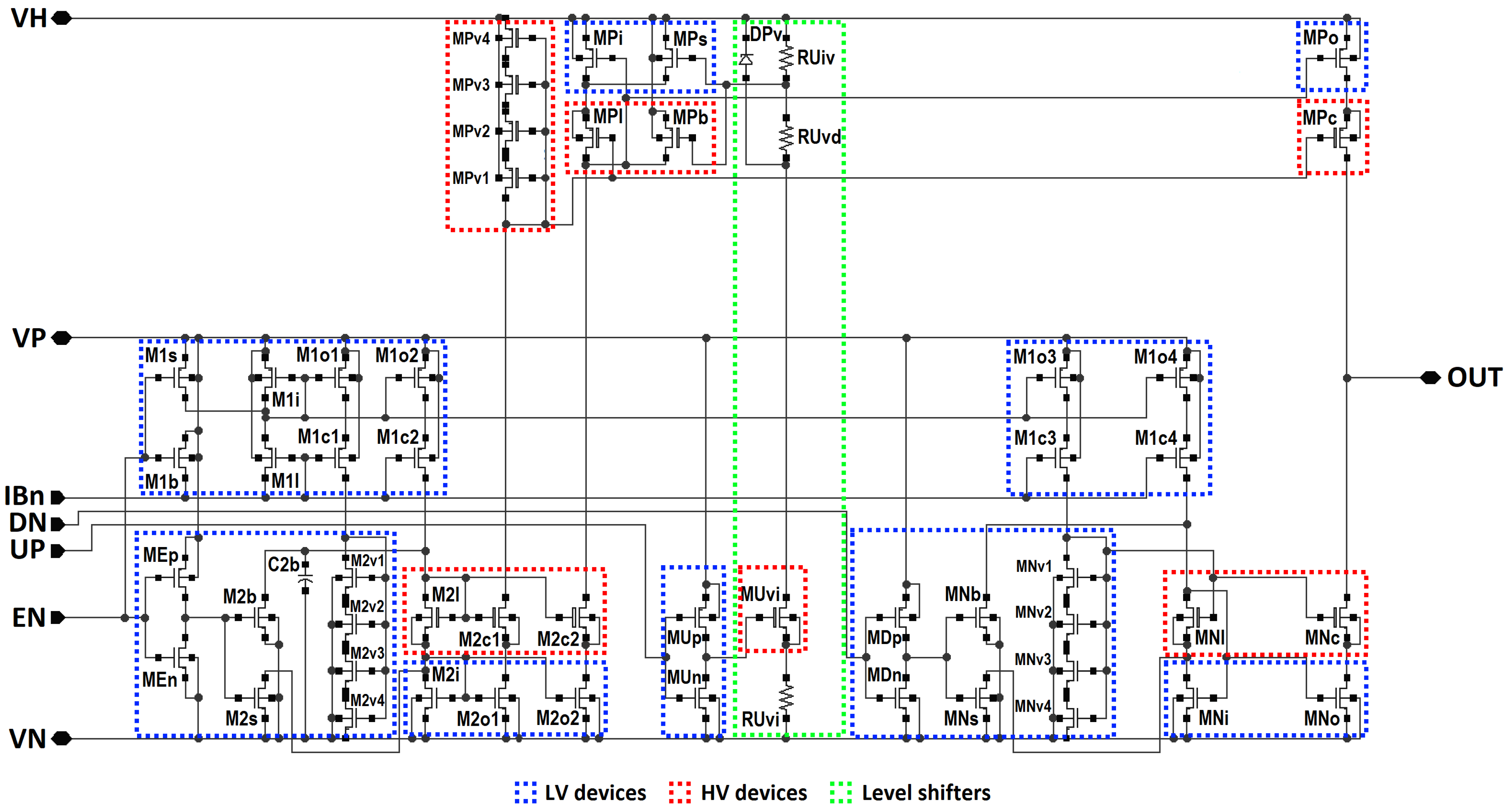
Figure 4 presents a schematic of the discussed waveform generator. MV MOS transistors have slightly different symbols; however, due to their general similarity, they are marked in Figure 4 with red dotted boxes. Overall, there are 41 NMOS and 10 PMOS transistors in the designed circuit, of which 6 NMOS and 7 PMOS devices are HV ones.
As shown in Figure 4, the HV trapezoidal waveform generator consists of a chain of LV and mixed LV and MV current mirrors biased with the external input current IBn copied and provided to the output current mirrors. The LV and MV mirrors are powered by the VP and HV power rails, respectively. These mirrors copy and amplify the input bias current four times before the source and sink currents are alternately provided to/from the output capacitor. The EN input is driven with a logic enable signal. If the EN input is low, input currents of the PMOS M1 mirror (consisting of M1i, M1l, M1o, and M1c transistors) and the following NMOS M2 mirror (consisting of M2i, M2l, M2o, and M2c transistors) are shorted to the VP and VN power rails, respectively. These short-circuits or bypasses are implemented with M1s and M1b transistors in case of the M1 mirror, and by the MEp/MEn inverter and M2s and M2b transistors in case of the M2 mirror. The sourcing and sinking phases of the operation are activated by two independent logical input signals named UP and DN that enable/disable operation of their related mirror similarly as in case of the EN signal. These signals define the start of waveform formation. When the output voltage reaches either the ground or HV supply level, the waveform voltage change stops regardless of the relevant logic signals [1].
The output node OUT (the one connected to the output capacitor) is the only one in the generator on which high-voltage swings are present. The majority of current mirrors in the circuit operates at steady LV conditions. The operation phases of the generator are switched by bypassing the input currents of the output current mirrors MP and Mn directly to the ground and high-supply nodes. The XDM10 process makes it possible to place LV logic circuitry between the MV/HV supply (the VH rail) and a virtual ground node level that is no more than 5 V lower than the VH voltage. This property of the XDM10 process helps shift the logic values to the circuitry that controls the operation of the high-side (current sourcing) output current mirror. The author proposed several topologies for logic shifters in the LV-to-HV range [30]. However, to simplify the circuitry, no virtual ground function block is implemented. Thus, the logic signal for controlling the high-side output mirror must be provided differently.
As in the case of the level shifters presented in [30], the applied function is based on passing or blocking a current flow from the LV to the HV side of the shifter (green box in Figure 2). The LV control signal is converted from the voltage logic to the current flow with MUvi transistor and RUvi resistor. Logical zero means no current flow. The flowing current passes through the RUiv and RUvd resistors connected to the HV rail and bypassed by the DPv Zener diode. The current flow causes a voltage drop in the series-connected resistors that is large enough to open the Zener diode that stabilizes the voltage on the series-connected resistors. The RUiv and RUvd form a voltage divider, and the division voltage is sufficiently lower than the HV supply level to turn the gate-connected MPs and MPb transistors into conduction mode, and thus bypass the input current from the MPi and MPl transistors that form the input of the high-side output mirror. Generally, the author found the application of current-mode signal processing very beneficial to avoid HV swings in HV circuits and systems. As presented in [30], current-mode processing was successfully utilized in a variety of HV function blocks, including unity gain buffers, waveform generators, level shifters, voltage-to-current converters, switches, and specialized edge-rounding circuits [7] for further (if needed) processing of trapezoidal waveforms.
Structure and operation of the direct predecessor (no. 2) (Figure 3) of the discussed generator (Figure 4) is virtually identical to the latter one. The structure of an early attempt (predecessor no. 1) is simpler. There is no logic level shifter, because the current bypassing functionality is not implemented in the output HV current mirrors MN and MP, but instead in preceding LV mirrors MU and M2. The resulting structure is very simple and has short current mirror chains for both the low- and high-sides of the generator. Unfortunately, if the charging/discharging currents are bypassed to the LV supply and ground nodes in the LV mirrors, the transistors of the output HV current mirrors are at the verge of conducting state, and MOS sizing mismatches can produce weak current flows and distortion of the generated waveforms. The output mirrors are partially composed of MV/HV MOS transistors that offer inferior matching capability, which can deepen this problem. This outcome resulted in the generator structure presented in Figure 3 and Figure 4.

3. Test Results

3.1. Test Bench Structure

Simulations of the waveform generator discussed in this paper were performed using the Cadence Virtuoso IC Design Environment version IC6.1.7-64b.500.12 provided by Cadence Design Systems, Inc. (San Jose, CA, USA) with the XDM10 design kit rev. 4.0 provided by X-FAB and the H35B4 design kit ver. 4.10 provided by AMS. All simulations presented were performed with application of the mentioned OCC (operation condition check) device models that enable constant observation of SOA fulfillment. The generator was fully laid out with the intent of sending it into production. However, the results presented in the article are simulation tests based on the design schematics and post-layout parameter extraction, along with their comparison.
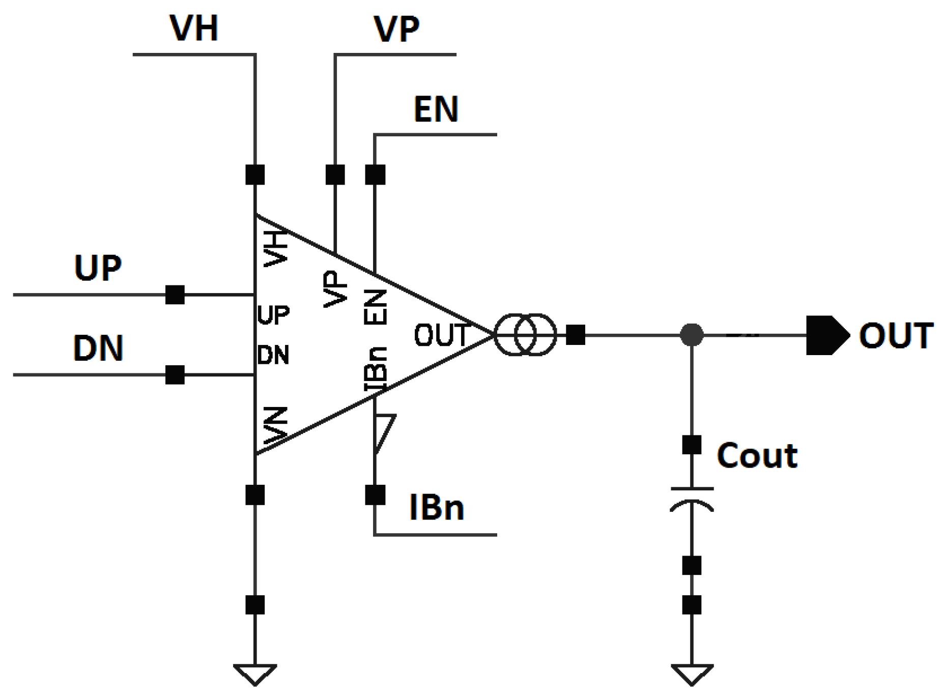
The main test bench is shown in Figure 5. The system consists of the generator loaded with the output capacitor Cout. The generator is connected to LV and HV supply rails (VP and VH, respectively) and ground node VN. The external input bias current source is connected to the IBn current input, and two external counterphase logic signals are provided to UP and DN inputs to drive the HV output current mirrors. As a rule, the designed waveform generator was simulated with 5 V for the LV and 18 V for the HV supply voltages.
To focus the analysis solely on the operation of the generator, the capacitor was implemented as an ideal element. In real applications, such a capacitor is replaced with series- or parallel-connected technology capacitors due to both the SOA requirements and the necessity of limiting variation of capacitance with the change in voltage between the capacitor sides. This phenomenon is possible in case of on-chip process-based devices, and can be more pronounced in case of HV applications. The capacitances of the generator transistors are taken into account in the performed simulations, including post-layout parasitic ones.
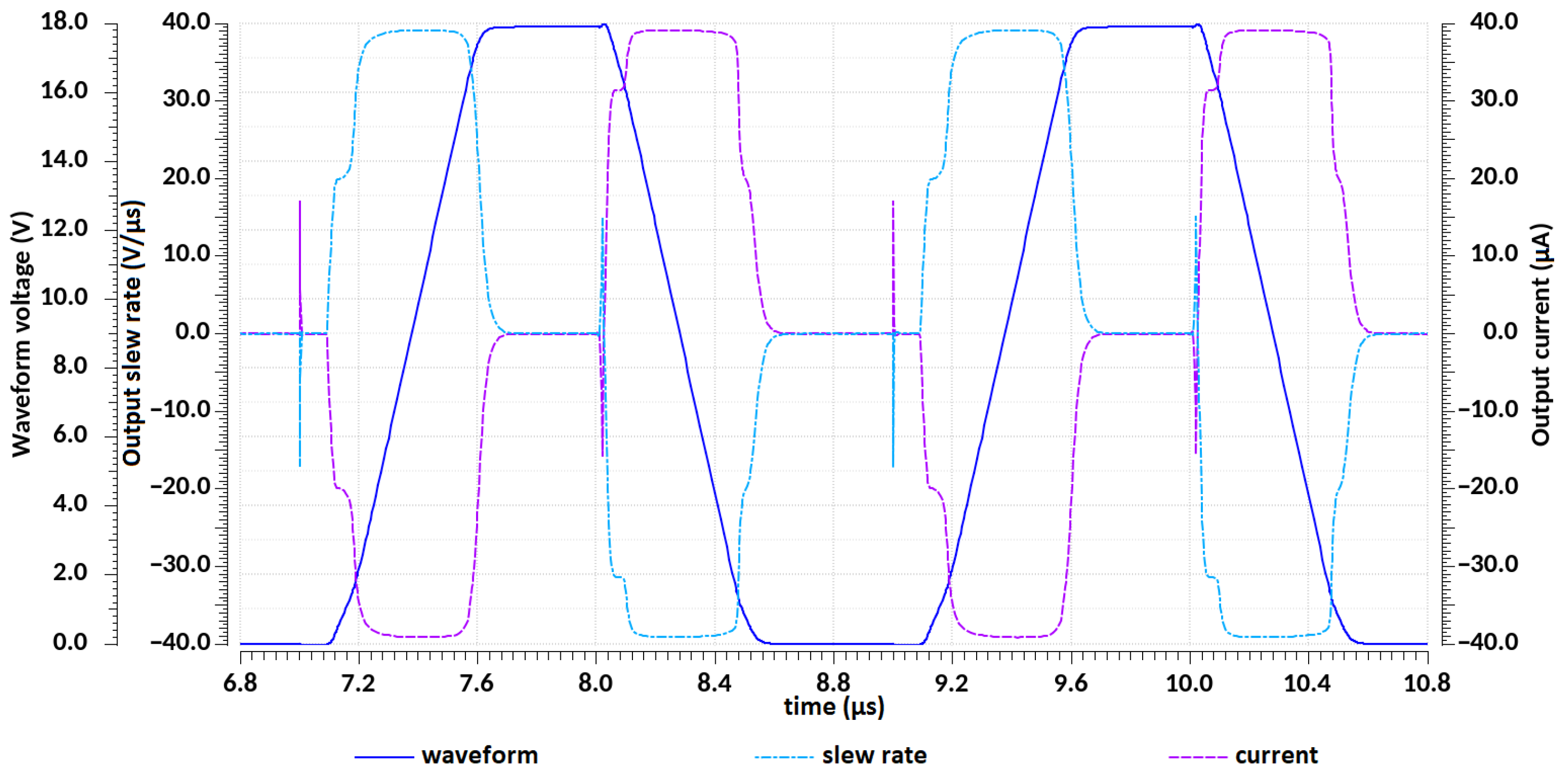
The basic operation of the generator schematic was confirmed in the introductory simulations presented in this section. The application of a basic control scheme of a single external IBn bias current and two 500 kHz counterphase logic signals results in the proper formation of the output. The main problem at higher frequencies is related to fast transients in the output stage, which requires more robust safe operating area protection. This in turn tends to degrade overall operation of the circuit. Figure 6 presents an overview of the operation achieved for an input bias current equal 10 µA and the output capacitor of 1 pF. The curves show the output waveform, its slew rates, and output currents over time. It can be observed that because of the ideal nature of the output capacitance, the shapes of the output waveform slew rate very closely resemble the output current values.

3.2. Design of the Overvoltage Protected Generator

The initial simulations also revealed an expected problem associated with SOA violations. There are several points in the circuit that experience short-term OV (overvoltage) events, including potentially destructive ones. Such problems must be solved using additional circuitry, which increases the design complexity. This problem is known and can be solved in various ways. There are several propositions of structures capable of both detection and action against overvoltage (whether negative or positive), as presented in [31,32]. The circuit presented in [32] protects an HV switch, i.e., a circuit with applications related to HV switches proposed by the author in [30].
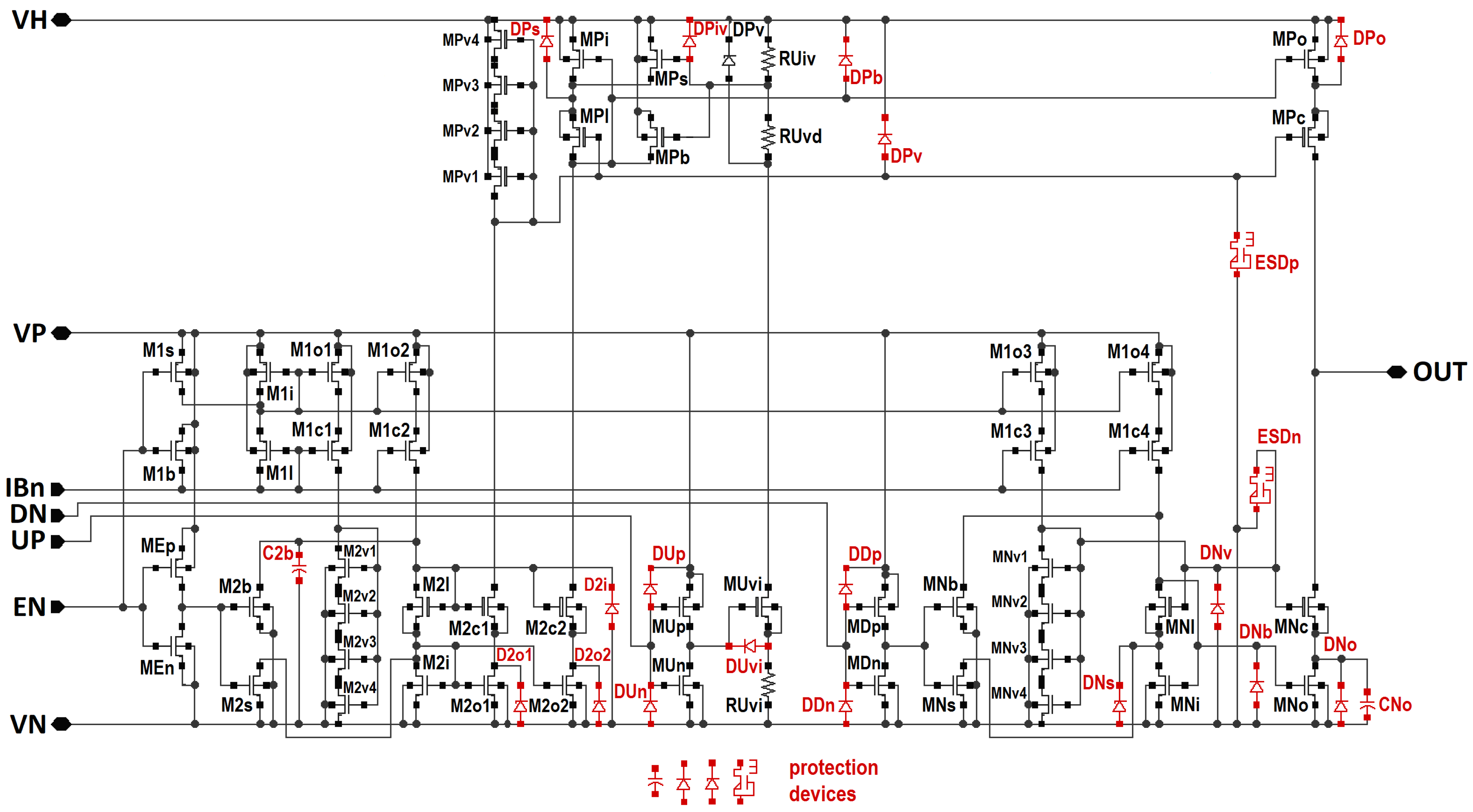
The number of nodes in the designed generator that need overvoltage protection suggests the application of simple solutions, as discussed in [30] and implemented in [1]. Fortunately, the designed circuit operates mainly under steady conditions, except for the two output HV current mirrors. Thus, similar generator topologies can be equipped with simple protection means, such as PN and Zener diodes. They are implemented to prevent drain-source or gate-source overvoltages. The generator schematic with a complete set of overprotection devices is presented in Figure 7. It can be observed that a total of eight PN diodes, four Zener diodes, and two capacitors are used on the low (ground) side of the generator, and three PN and two Zener diodes protect its high (HV supply) side [1]. Additionally, there are two devices implemented to guard gates of the MPc and MNc HV MOS transistors that are exposed to high-voltage swings at their drains. They are named ESDp and ESDn, respectively.
This addition is the result of consultation with X-FAB engineers and was suggested as a precaution against possible voltage surges from the source outside of the generator itself. Such phenomena may occur if the generator output is at the end of its signal-processing path and connected to the IC output or pad. The presence of a capacitor at the output of the generator helps stabilize the voltage levels, but it may be insufficient. In addition, if the output capacitor is considered to be external to the IC comprising the generator, the implemented ESD devices need to follow the ESD (Electro-Static Discharge) rules typical for IC pins to ensure the safe operation of the generator. These rules include modified sizing and separation of laid shapes, as well as requirements for interlayer connections. These much stricter layout rules are not covered by the design kit itself and are presented only in the form of documents provided by the foundry. In fact, these two overvoltage structures are scaled-down derivatives of the ESD structure, which accompanies most of the HV input and output pads of the IC, including the discussed generator.
The importance of proper protection against ESD is well known, and methods to increase the ESD immunity of active devices have been discussed [33], including techniques focused on HV technologies [34,35]. The main stress is of proper design on IO (Input–Output) structures of ICs, especially in the case of HV technologies [36,37].
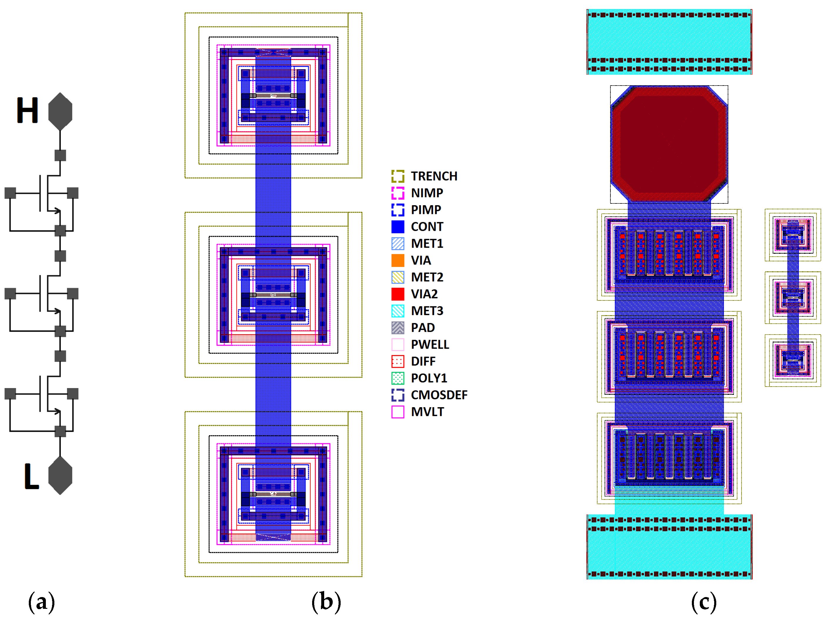
Both the original IO ESD structure and the scaled-down version for internal use were designed by the author due to aforementioned requirements not met by any components provided with the design kit. These structures are presented in Figure 8. They share the same schematic of the three series-connected transistors that form the diodes. They just use different transistor sizing, and thus different shapes and sizes of their layouts.
The modified schematic with additional OV and OV/ESD devices passed the SOA check tests for startup, operation, and shutdown and became the basis for the final (OV protected) layout of the generator. Thus, three main design stages are present and available for comparative analysis. Such an analysis was performed to study both the properties of the designed generator and their alterations due to the addition of OV and OV/ESD devices and process of laying out the fully protected schematic.

3.3. Introductory Tests

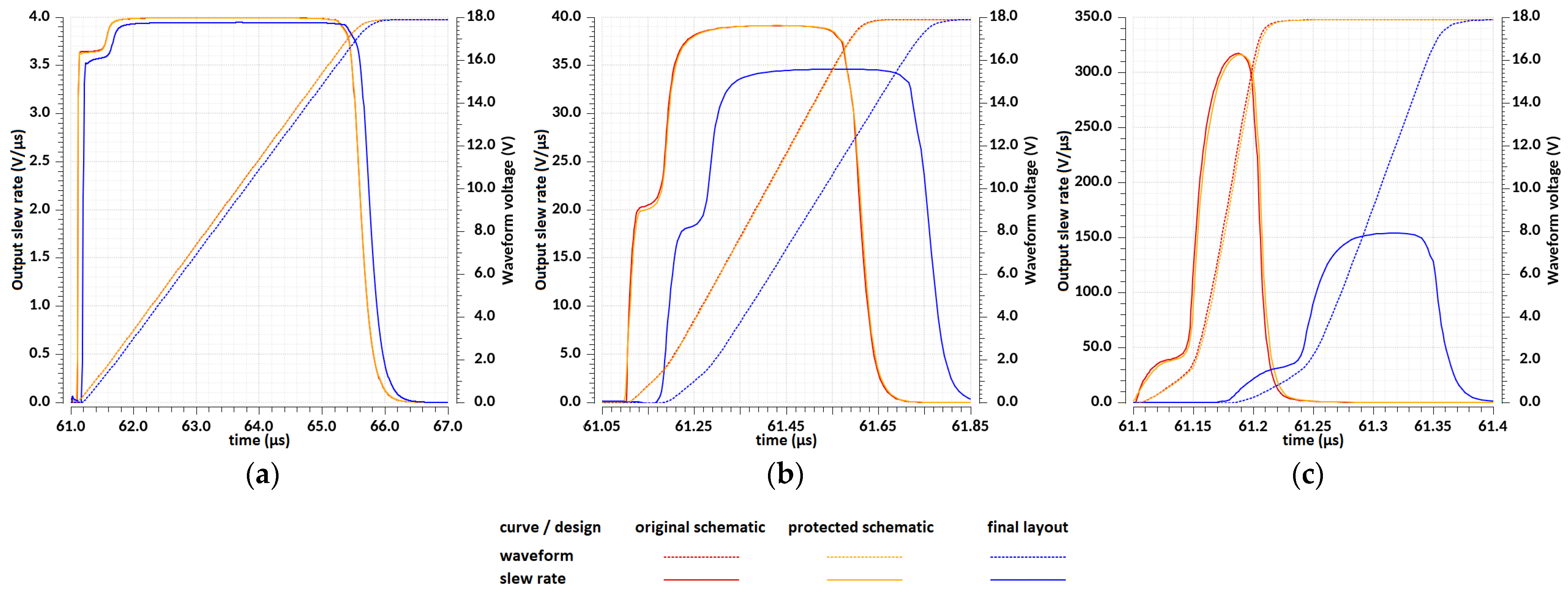
First, several time-domain simulations were conducted to observe the operation of the proposed waveform generator. Figure 9 and Figure 10 present rising and falling edges of the generated waveforms and their related slew rates for the input bias current equal 10 µA (the bias current originally intended for the generator) and the output capacitor of 10, 1.0, and 0.1 pF. These results are presented for all three stages of the design: the original schematic, the protected schematic, and the final layout. Table 1 lists the slew rate error values calculated for these simulations.
It can be observed that for output capacitors equal to 10.0 pF, the operation of the generator can be considered acceptable for all three design completion stages. The obtained slew rate values are very close to the expected ones for vast majority of the voltage span of the output waveforms (the slew rate error less than 2%). The slew rate error presented in Table 1 is defined as a percentage of the difference between the simulated value and expected one, based on the value of the output capacitance and the output current. The slew rate errors for the original and protected schematics were below 0.3%. For the final layout, the slew rate error was equal to 1.35/1.78% (for the rising and falling edges, respectively). The waveform slew rates observed for the 1.0 pF output capacitor were very close to the expected values for both the original and protected schematics (slew rate error equal about 2%). However, the slew rate for the final layout has an error of up to 15%, which is difficult to consider as acceptable. In the case of the fastest output waveform formed on the integrating capacitor equal to 0.1 pF, the slew rate error for the original and protected schematics was approximately 20% and over 60% for the final layout waveforms. The generator working with a 10 µA output current and 0.1 pF produces the most distorted output due to the excessive slew rate of the output waveform.
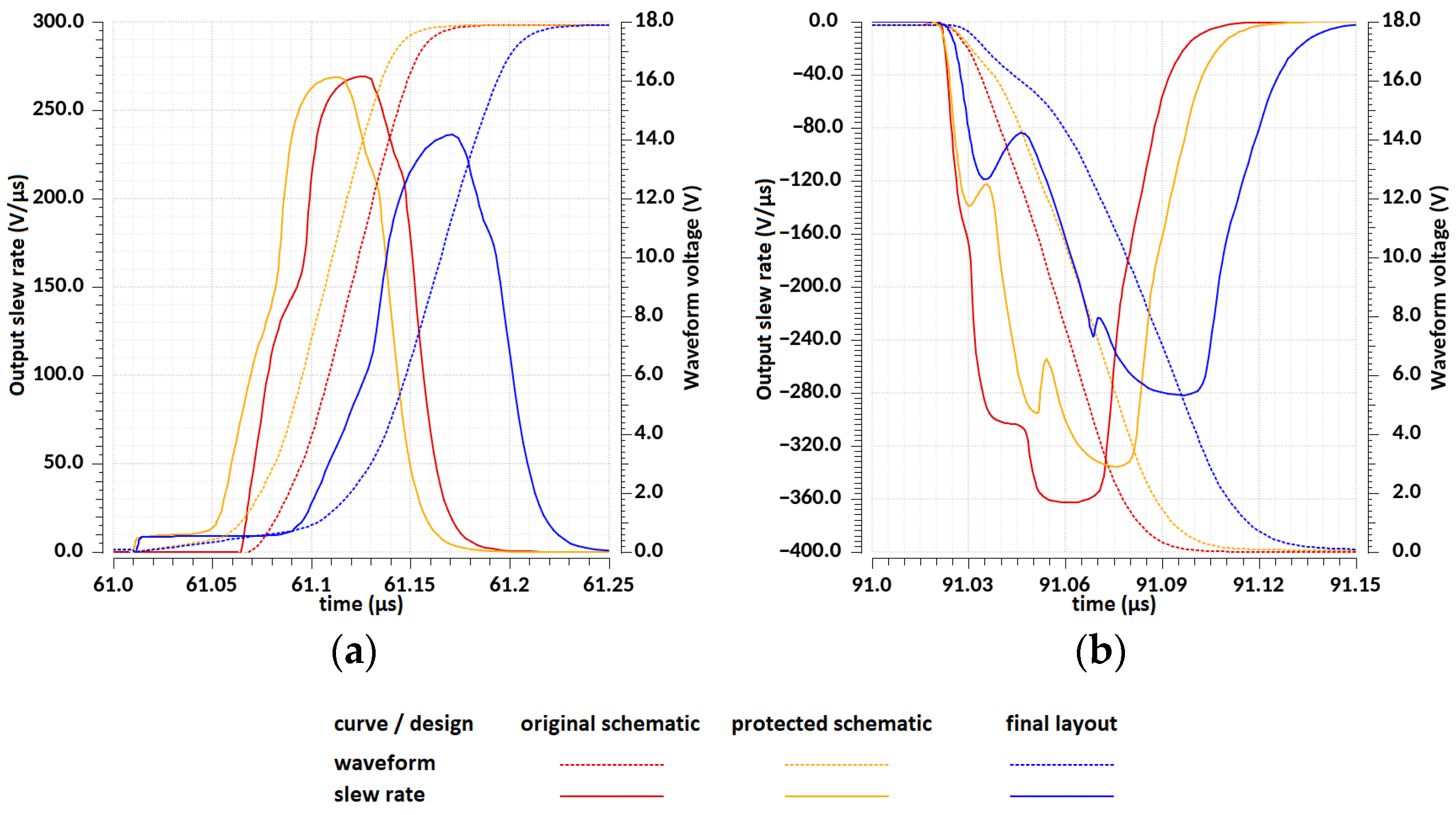
Another analysis was performed for 100 µA output current and a 1.0 pF output capacitor, which should result in an identical waveform slew rate as that of the generator working with 10 µA output current and a 0.1 pF output capacitor. The time plots for this new test version are presented in Figure 11 and Table 1. This configuration shows more visually distorted slew rate shapes, but the slew rate error increase between the original schematic and final layout is much weaker than in the case of the three former configurations. Although 10 µA/0.1 pF is equal to 100 µA/1.0 pF, Figure 9c, Figure 10c, and Figure 11 clearly show that the operation of these two generator test variants is different. Although the slew rate errors were lower for the latest generator variant, differences in operation for the original and protected schematics are discernibly different, which was not observed in the former simulations.

3.4. Parametric Tests

All the results obtained for the arbitrarily selected values of the input bias current and the output capacitor show the need to perform a more systematic analysis of the generator operation.
As mentioned above, the designed generator was originally intended for operation with the input bias current equal to 10 µA. Introductory tests show that proper output waveforms can be properly formed with such biasing only if the capacitor value does not cause too fast voltage swings at the output (Figure 9a and Figure 10c). The operation of the generator biased with 100 µA current and loaded with 1 pF output capacitance shows significant distortions of the output waveform (Figure 11a,b). They can be attributed to the excessive value of the bias current, as the same generator loaded with the same capacitance but driven with the intended 10 µA current works much better (Figure 9b,c). These observations demonstrate the necessity of checking the capabilities of the generator internals, that is, the current signal path.
The first session of the test simulations was conducted for a fixed 1 pF value of the output capacitor and a variable input bias current in the range <0.1, 1000> µA, with 10 values per decade. For clarity, some of the figures present results obtained for four values per decade. The capacitor value is sufficiently large to not cause significant deterioration (transient phenomena) of the output waveform for practically applicable (low enough) bias currents.
Simulations were always conducted for all three completion stages of the design, i.e., the schematic, protected schematic, and final layout cell views. The time-domain simulations were conducted for the test setup presented in Figure 5.
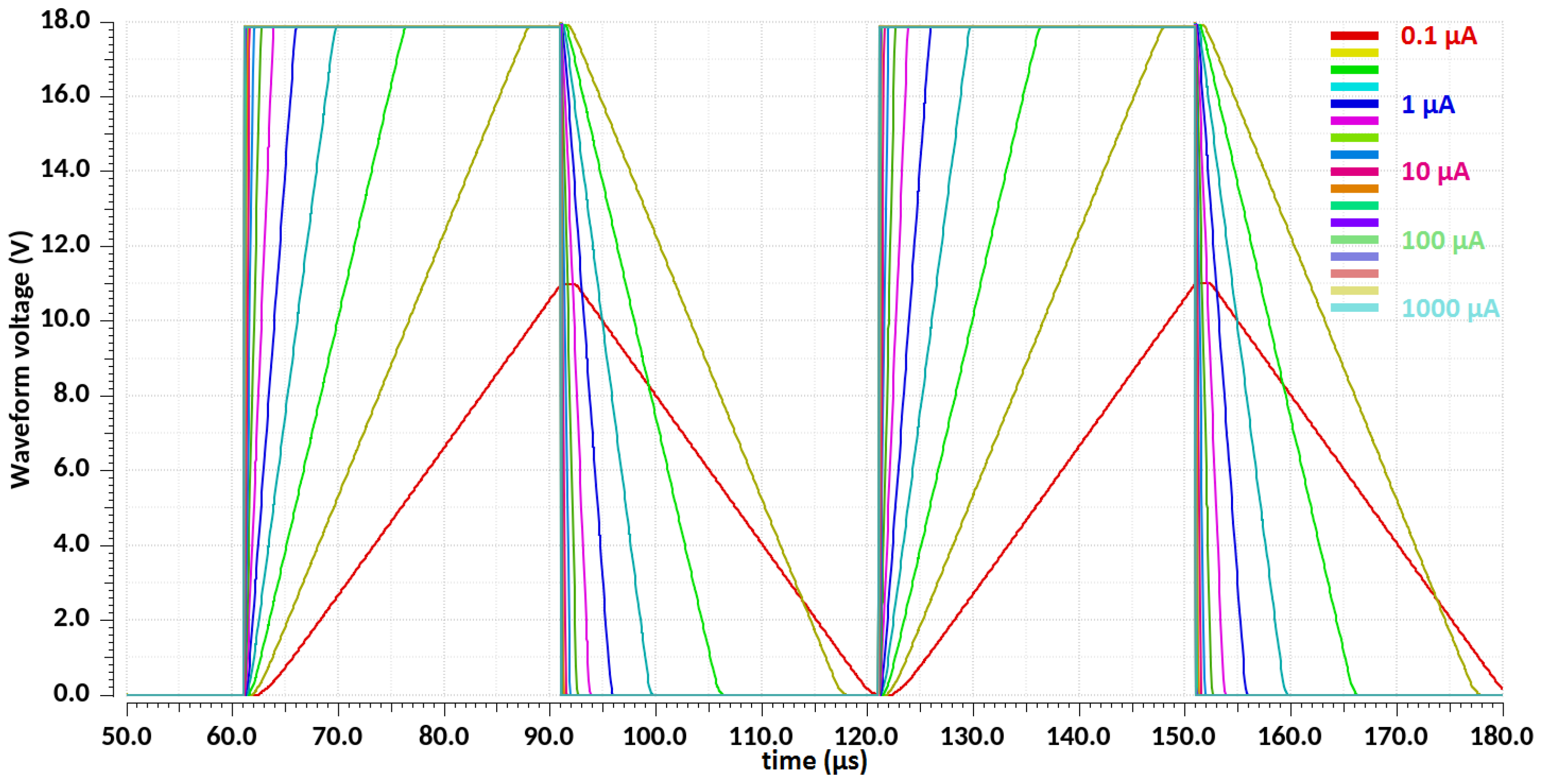
The results in Figure 12 show the output waveforms for the entire range of the input bias current.
Figure 13 and Figure 14 show the zoomed-waveform slew rate and output current for a single rising and falling waveform edge, respectively.
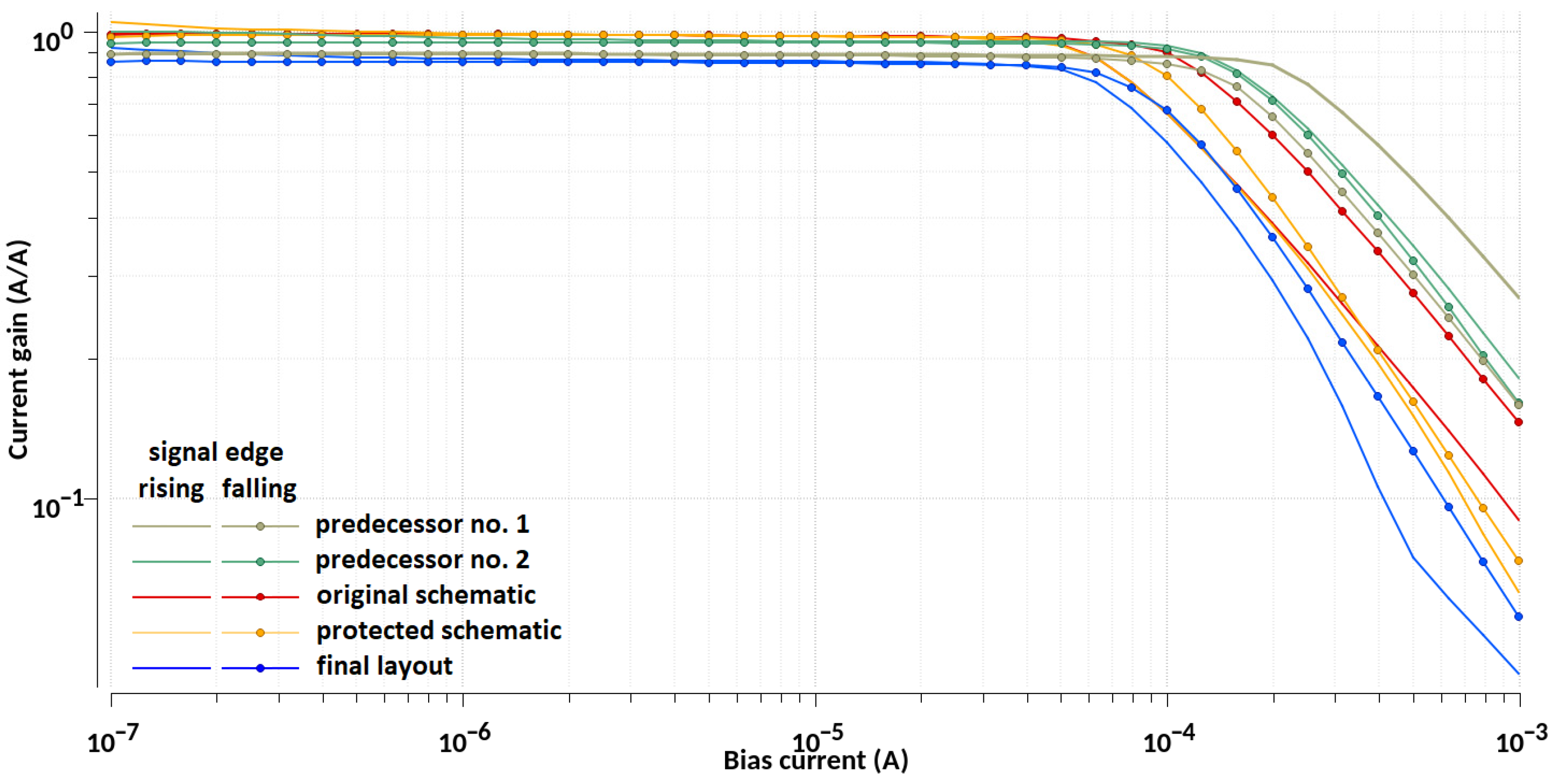
Figure 15 presents the normalized (to unity) gain of currents provided by the low- and high-side HV current mirrors all tested designs and waveform edge types, including both predecessor schematics. The maximum values at plateaus of the output current transients were extracted, divided by 4 (the current gain of the generator), and presented as functions of the input bias currents.
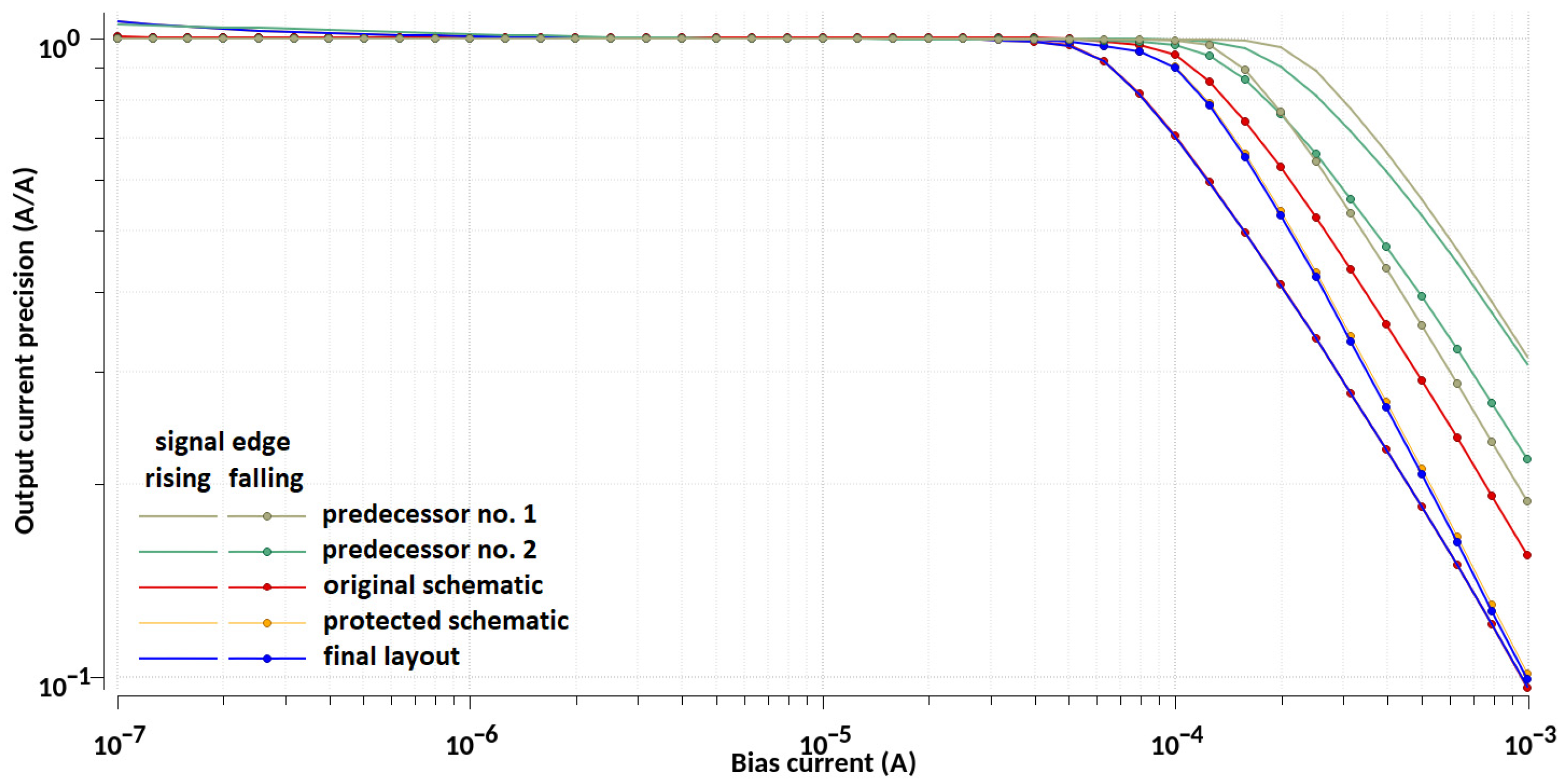
Similar simulations and plots were conducted in the DC and frequency domains. Figure 16 presents simulations of the current efficiency of the generator for all tested designs and waveform edge types. The main test bench had a DC voltage source instead of the output capacitor. This voltage level is equal to half the supply voltage; thus, both output mirrors can operate normally under similar output conditions.
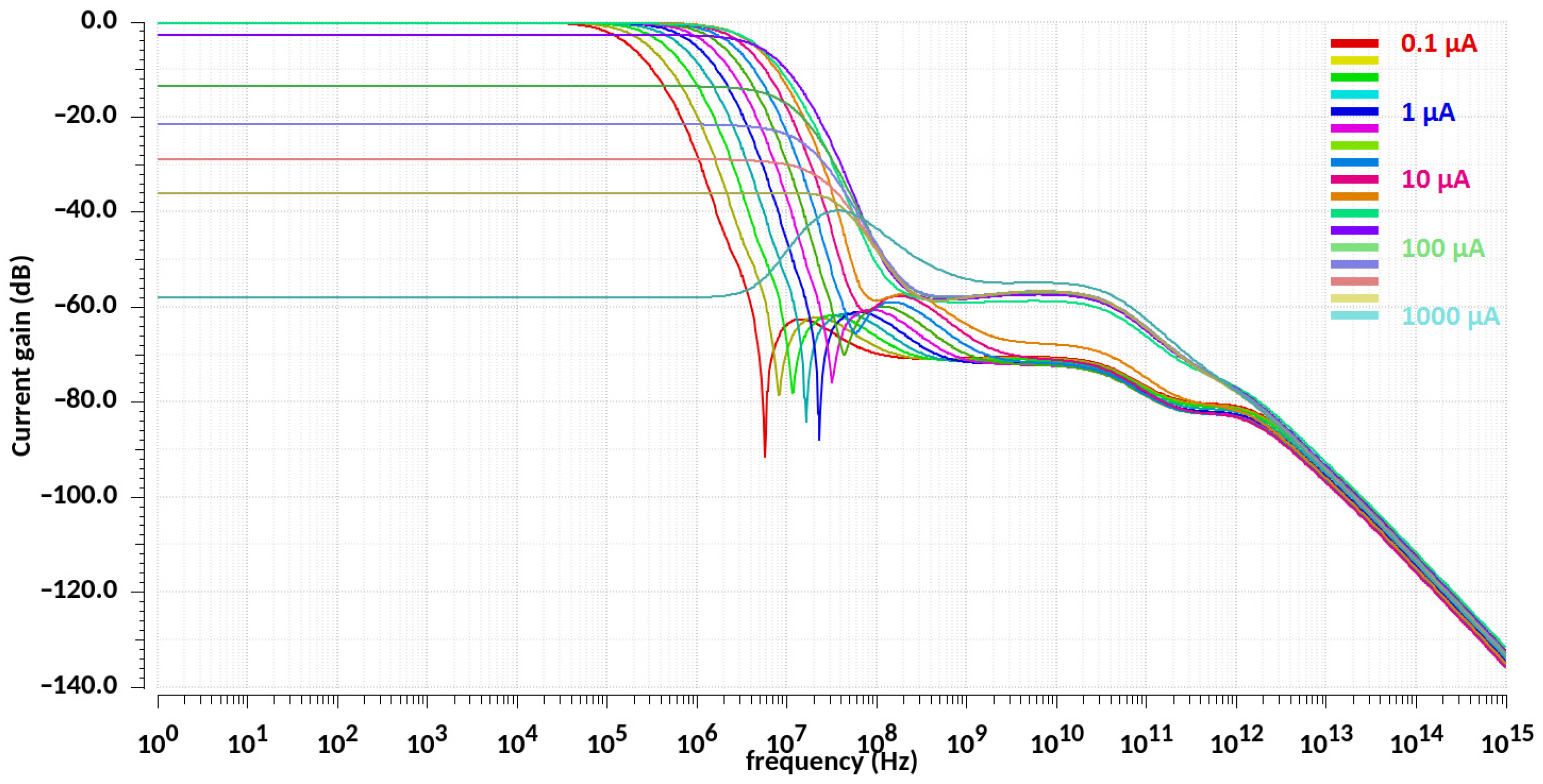
Figure 17 represents an attempt to replicate the same dependence with the use of AC (Alternating Current) simulations. These results are based on the frequency responses of the output current mirrors of the generator (line one presented in Figure 18) obtained for the aforementioned range of input bias current values.
Maximum usable bias currents (defined as causing less than 10% slew rate error) are presented in Table 2, which summarizes the results presented in Figure 15, Figure 16 and Figure 17.
The results of the AC simulations (Figure 18) were also used to plot the dependence of the output current bandwidth on the input bias current, as shown in Figure 19. The corresponding Table 3 lists the maximum bandwidth values for each tested design stage with information on the corresponding bias current for which these maxima are achieved.
Another approach to scrutinize the properties of the designed waveform generator is a parametric test, in which the slew rate of the output waveforms is expected to remain constant, but its value is achieved with different values of the bias currents and output capacitors. This approach can be regarded as an optimization method for generating a specific predefined waveform. The waveform is defined by its frequency, fill factor, and slew rates. To maintain the slew rate constant, the quotients of the bias current and output capacitance must remain constant. From here on, this quotient is referred to as the multiplier of the current and capacitor values. A multiplier of 1 means that the input bias current is 1 µA and the output capacitor is 100 fF.
This second test session was conducted for the multiplier value in the range of <0.1, 1000>, with 10 values per decade. It is worth noting that such a multiplier range results with the range of the input bias current equal <0.1, 1000> µA, which is the same as in the case of the former test session. Simulations were always conducted for all three completion stages of the design.
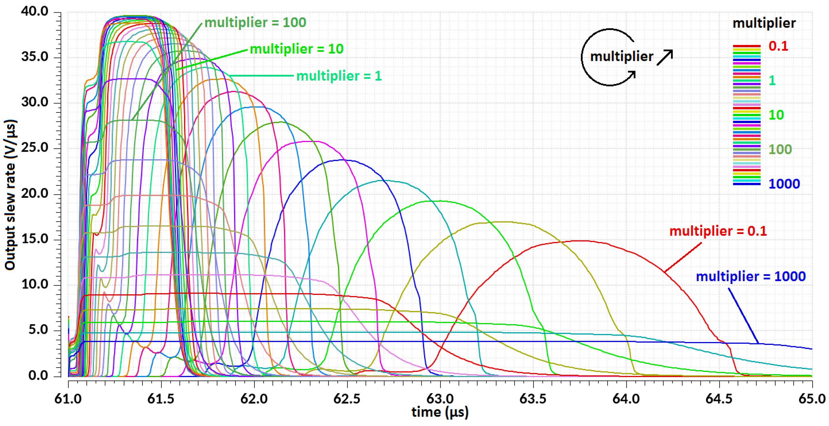
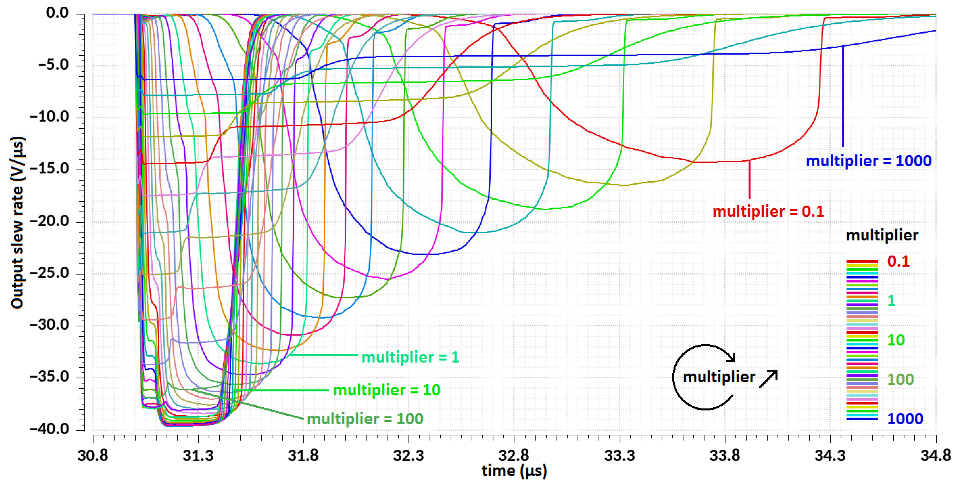
Figure 20 and Figure 21 show plots of the zoomed-slew rates for single rising and falling edges of the output waveform.
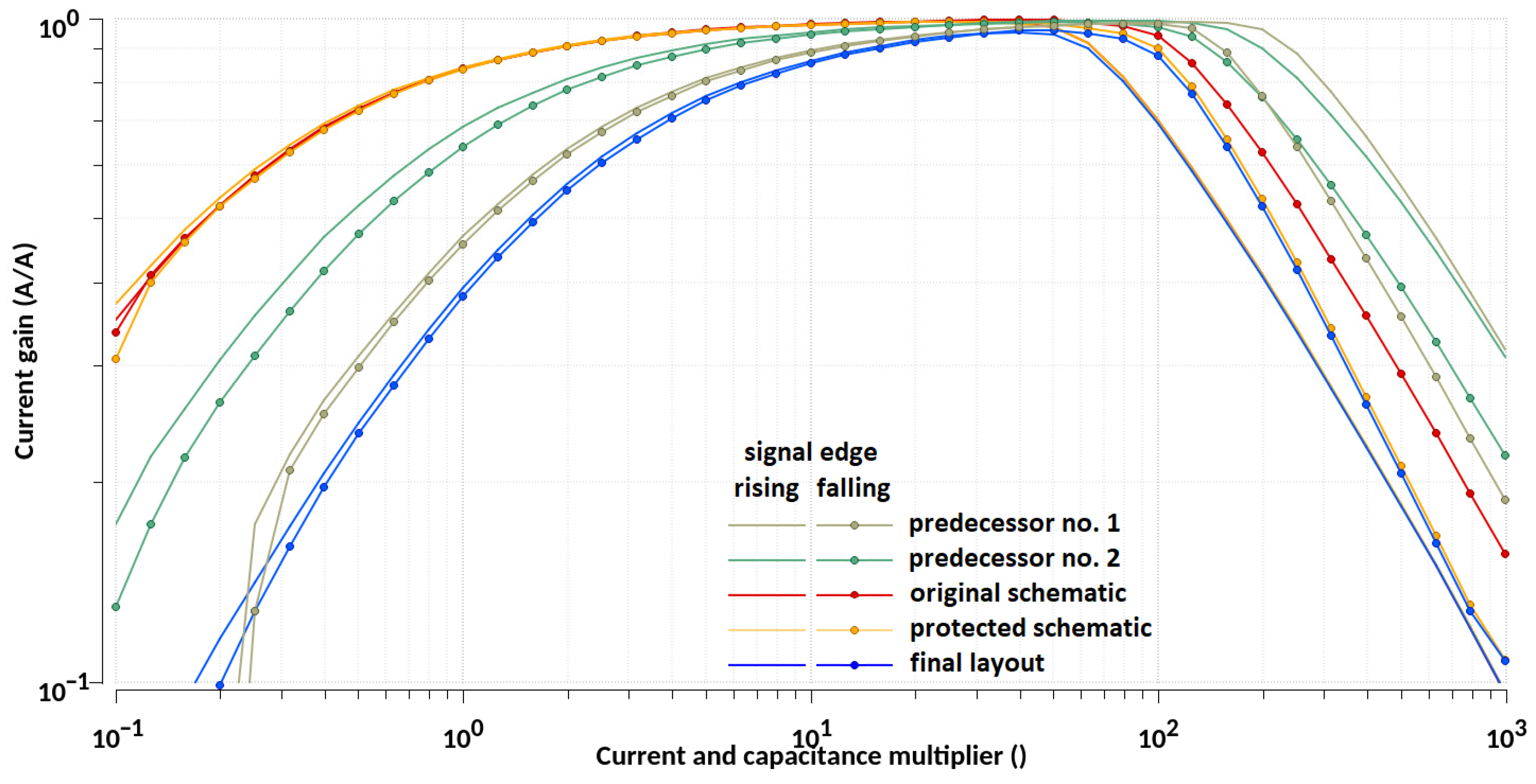
Figure 22 presents the dependence of the efficiency of transmission of the input bias current transmission to the output HV current mirrors (normalized gain) on the multiplier, based on transients of the output currents for all tested designs and waveform edge types.
Table 4 presents the minimum and maximum usable bias currents (defined as ones causing less than 10% slew rate error) based on the results presented in Figure 22.
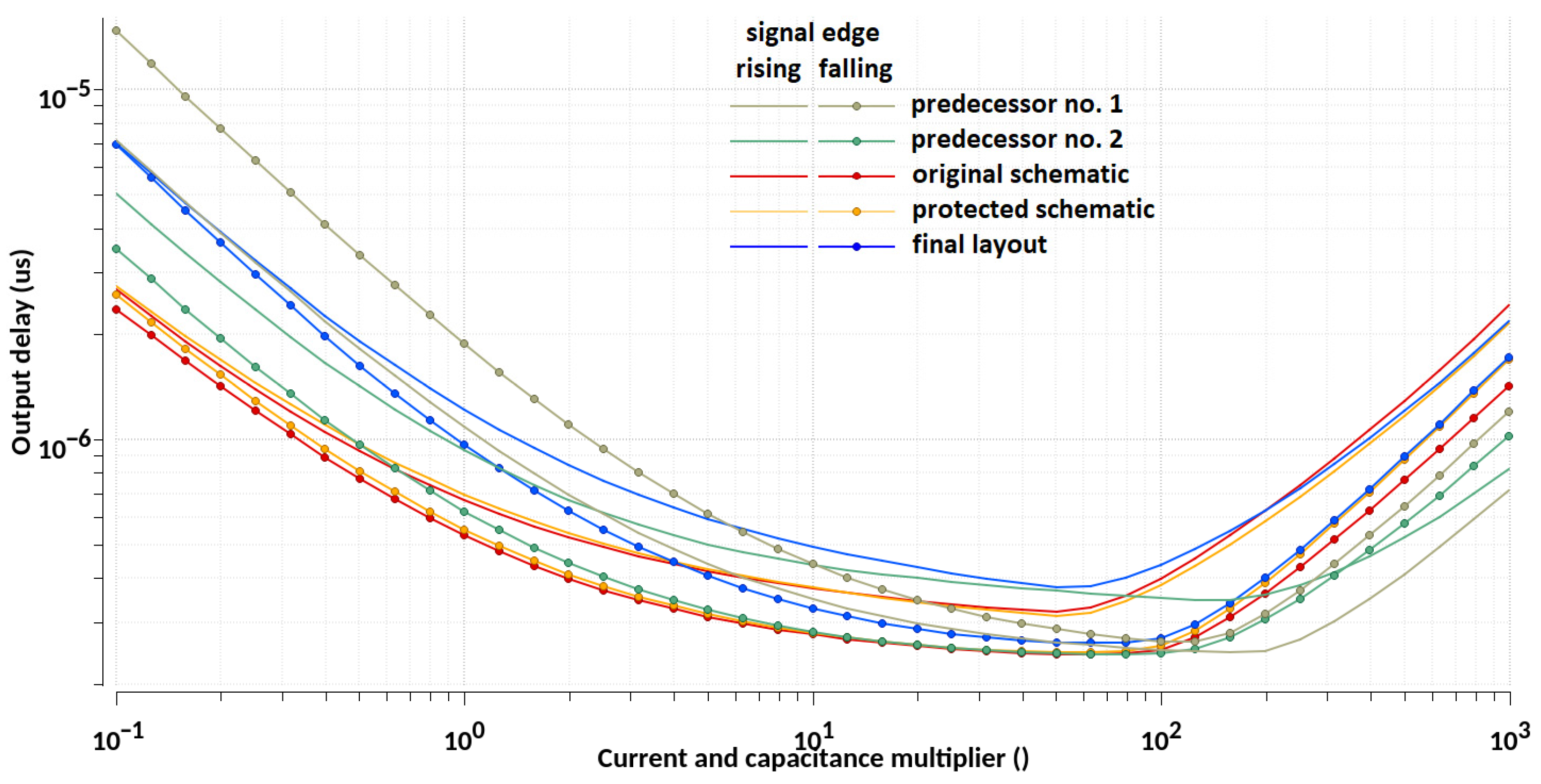
Another tracked parameter is the dependence of the output waveform delay on the multiplier in the defined range. Figure 23 plots the results for the three design versions. This delay is defined as the delay between the input logic signals used to control currents flowing through the HV output current source and the trapezoidal waveform produced by these currents and the output capacitor.
Table 5 lists the minimum delay values obtained for all the tested design stages along with the corresponding multiplier values of the 1 µA bias current and the 100 fF output capacitor.

4. Results Discussion

4.1. Test Session for Constant Output Capacitor

The results presented in Figure 9, Figure 10 and Figure 11 are related to the introductory tests that were discussed in the previous section and gave rise to two sessions of detailed parametric tests. The results of these two sessions are discussed in the following section.
The first test session was based on simulations of the generator loaded with constant 1 pF output and biased with current in the range of for <0.1, 1000> µA.
Figure 12 shows wide range of waveform shapes that can be produced based on value of the input bias current. The operation quality of the generator can be determined by analyzing the plateau value of the output waveform slew rates. It can be observed that four orders of current magnitude result in waveforms ranging from virtually square to triangular. Another important factor is the overall shape of the slew rate curve. However, if it is substantially distorted, e.g., there is no properly defined plateau as in case of very small bias current, it is difficult to consider the obtained output as a trapezoidal waveform.
More insight can be obtained by observing the waveform slew rates and their relevance to the output currents. According to the results shown in Figure 13 and Figure 14, the slew rate and output current curves strictly correspond to each other, as should be in the case of proper current integration on the ideal capacitor. The shapes of the slew rate plots differ greatly depending on the input bias current. In fact, Figure 13 and Figure 14 present only magnified views of the slew rate (and the output current) plots. In the case of lower slew rates, only a beginning part of their plateaus is presented, whereas high slew rate curves are presented in full. These plots show that there is a range of input bias current values for which the slew rate plots possess proper plateaus. Above this range, visible deterioration of the slew rate plots can be observed in terms of both the shape and value of the plateau.
The currents used in the currently discussed simulation test ranged over four orders of magnitude, while the generator design remained the same. All current mirrors in the generator copy or multiply the input bias current. The same input current is used in all biasing structures in modified cascode mirrors so that their bias voltages can adjust to the current flow. The limiting factors for all these current mirrors were the current densities in the transistors (with related voltage drops in their channels) and the LV supply level. Both these factors can lead to limited and insufficient voltage space for the mirrors that operate with high and increasing input bias current values, thus leading to the mirror saturation.
It can be seen that the current gains/efficiencies presented in Figure 15 and obtained for the rising edge of the output waveform start to decrease for lower current values than in the case of those obtained for the falling edge. This observation was valid for all three tested design stages of the discussed generator. The rising waveform edge is formed by the HV output mirror comprising the LV and MV PMOS transistors based on the less effective hole conduction, which may contribute to the observed effect in relation to the transistor sizing of NMOS and PMOS transistors. Moreover, for both rising and falling waveform edges, the best generator operation was obtained for the original schematic, a slightly limited one for the protected schematic, and the most limited was obtained for the final layout. It can be observed that the influence of OV protection devices is already visible for the protected schematic, which is more evident in the layout. It can be interpreted as a progressing limitation of input bias currents for which the output currents (forming both rising and falling edges of the output waveform) reach their expected values.
In case of the predecessor schematics, the results are reverse. The current gain for the rising waveform edge starts to decline for higher bias currents than in case of the falling edge. Moreover, the maximum current values for which the current gain is acceptable are higher than in case of the discussed generator. This effect shows that different transistor sizing and properties may lead to different results and that these issues can and should be the subject of further optimization.
An unexpected phenomenon causing such limitations was observed in both the low- and high-side output mirrors of the discussed generator (MN and MP). During quick swings of the output current and voltage, current flows occur between the HV output cascode transistors MNc and MPc and the drains of one of the auxiliary bias setting devices MNv1–4 and MPv1–4, respectively. These current flows cause gate recharging of the MNc and MPc HV output cascade transistors in the low- and high-side output mirrors and alteration of the output current flow. The phenomenon is more noticeable in the protected schematic because of the presence of protective devices (ESDn an ESDp) connected to the gates of these HV output cascode transistors. The presence of parasitic components in the layout netlist further deteriorates the shape of the output waveform.
The transient (Figure 15) and DC (Figure 16) plots show similar effects of current gain reduction. Notably, there is no deterioration in the operation for the results obtained for the final layout of the generator compared with those obtained for the OV-protected schematic. Clearly, DC simulations do not include any capacitors, including parasitic devices. In addition, there is a discernible increase in the current gain/efficiency for very low input bias current values obtained for the protected schematic and the final layout in the case of the rising waveform edge only. The same phenomenon can be observed in Figure 15 for the same stages of the circuit design and waveform edge. This phenomenon originates in a low-side (related to ground node) M2 NMOS current mirror connected to the input of the high-side (related to the HV supply) MP cascode current mirror. The low-side M2 mirror encounters excessive drain-source voltages in the LV output main transistor M2o2, and its drain (and source of the HV output cascode transistor M2c2) is protected by the presence of a Zener diode D2o2. Thus, this diode is connected in parallel to the LV output main transistor and adds its leakage current to the current flowing through the output cascode transistor Mc02. The larger the current processed by the low-side mirror M2, the weaker the influence of the Zener diode D2o2. The low side of the HV output current mirror MN is also equipped with Zener diodes for the main LV transistors of the mirror. The difference is that there are two of them (DNs and DNo), one for each side of the mirror. Thus, the influence of these Zener diodes is nearly eliminated, as these diodes are connected in a symmetrical (mirroring) manner. Results for the predecessor circuits are similar as in case of transient simulations.
In case of small-signal AC simulations (Figure 17), the observed extra gain effect is not present. In addition, the AC simulation results are very similar to those obtained for the DC tests (Figure 16). Again, the results obtained for the final layout and the OV-protected schematic are nearly identical. Furthermore, the current path of the high-side MV PMOS current mirror MP responsible for the formation of the rising edge of the waveform is slower than that of the low-side MV NMOS current mirror MN responsible for the falling edge. The results obtained for the earlier circuits designed with the AMS H35B4 process are similar to those for transient and DC simulations.
According to results in Table 2, there is a consistent trend of higher currents with acceptable errors for the falling edge of the output waveform. The edge is produced by the low side of the generator, which is formed by LV and MV NMOS transistors. This effect is also exhibited by the results obtained in the DC simulations. This indicates the necessity of improving the high-side current path of the generator, which is responsible for forming the rising edge of the waveforms. The DC and AC simulation results showed that the maximum values of the applicable bias current mainly decreased between the original and protected schematics and only for the falling edge. This indicates the deterioration caused by the OV protection devices. An analogous effect for the transient simulations can be discerned for all three design stages, which further suggests parasitic effects coupled with the large-signal operation of the generator, instead of the small-signal evaluation provided by the AC simulation.
It can be observed (Figure 18) that both the gain and bandwidth change with the bias current. As mentioned before, the derived dependence of the current path through the generator is presented in Figure 19, for better clarity. Parts of the presented curves obtained for very high bias currents are clearly related to distorted DC conditions (excessive currents and voltages that lead to current mirror saturation) inside the generator. For a clear representation of their relationship, the highly distorted parts of the curves are removed. For low bias currents, an interesting trend was observed. The bandwidth of the generator current path increased as the bias current increased. Increase of the bias and mirror currents mean different operating points of the transistors that form a chain of current mirrors from the bias current input to the HV output stage, as well as a reduced influence of the side effects of the operation of devices that constitute the generator. Both capacitive effects (parasitic capacitances) and resistive effects (parasitic resistors and leakage current) can be accounted for here.
Table 3 shows interesting trends in the dependence of the maximum bandwidth on the bias current, based on the results of the AC simulation presented in Figure 19. The values obtained for the rising edge (that is, high-side PMOS based current path) were consistently three times lower than those obtained for the low-side NMOS-based current path. The main reduction in maximum bandwidths within the set of both rising and falling edges is observed between the OV-protected schematic and the final layout. Again, these results point to limitations of the high-side current path of the generator and the influence of parasitic components extracted from the layout view of the generator.
The results obtained for the predecessor no. 1 and 2 schematics show maximum bandwidth for higher bias currents, which is consistent with previous results. Additionally, these maximum bandwidth values are higher than in case of the results obtained for the rising edge of waveforms produced by the discussed generator. This effect can be attributed to both the NMOS and PMOS transistor sizing, as well as the fact that the predecessor technology (AMS H35B4) is 0.35 µm, while the discussed implementation of the generator is design with 1.0 µm process (X-FAB XDM10).
The result of the simulation analysis for a constant value of the output capacitor and a wide range of the input bias current is that, although there are minor side effects for very small current values, the main problem is related to high and excessive current flows that distort the operation of the chain of the current sources inside the generator and discernibly limit operation of the high-side current path of the generator.
That is an expected outcome, but another way of testing the waveform generator emerged and was introduced in the previous session, and is to be discussed now, as the waveform generators are often expected to provide a limited frequency and slew rate range of their waveforms.

4.2. Test Session for Constant Quotient of Output Current and Capacitor

Figure 20 and Figure 21 clearly show that there is a medium range of multiplier values for which the produced waveforms show properties close to those expected. The dependence of the output slew rate on the multiplier value is quite complex. As the output current flow was found very closely related to the presented slew rate curve, further analysis is based on the dependence of the output current (and capacitor) to the bias current. Thus, the currently discussed results can be directly compared to those obtained during the first test session (for the variable bias current and constant output capacitance). The resulting Figure 22 shows that the region of deterioration for very high and excessive currents can be observed, as in the previous test set. In fact, the high current or multiplier ranges are similar in Figure 15 and Figure 22.
However, in the tests with a constant I/C ratio, another region of current gain deterioration can be observed for very low multiplier values. The behaviors of the original and protected schematics of the discussed generator are very similar in this range. The operation of the generator operation simulated with the post-layout netlist with the extracted parasitics shows even more deterioration for small and decreasing multiplier values. This phenomenon can be attributed to the more demanding working conditions of the generator used in this test.
The values in Table 4 show only small differences between the original and protected generator schematics. The results for the final layout exhibit a substantial increase in the minimum and a limited decrease in the maximum applicable multiplier. These results again indicate the influence of parasitic components on the operation of the generator driven with very low current values.
Previously, the generator operated with a constant capacitor value. Therefore, the lower the bias current value, the slower is the build-up of the output waveform. Problems related to operation with low bias currents were mainly limited to the suboptimal operating points of MOS transistors in structurally non-symmetrical current sources and possible leakage currents. In the case of the present test session, the waveform generator was set to provide waveforms with constant slew rates regardless of the bias current.
A significant part of the generator presented in Figure 4 (the original schematic) and Figure 7 (the OV protected one) works with a constant DC current flow, while the HV output stage consisting of two mirrors MN and MP works with switched currents. Lower internal currents mean slower switching of the mirrors on and off because these mirrors operate in the presence of parasitic capacitors that need to be charged. All these effects lead to a modified operation of the discussed generator, which causes strange oblong shapes of the relevant slew rate curves presented in Figure 20 and Figure 21.
Trends in the results obtained for the predecessor schematics are similar to those observed for tests with variable bias current and constant output capacitor. The current gain is preserved for higher bias currents in case of the rising waveform edge and generally starts to decline for higher bias currents than in case of the discussed generator implementation.
However, in case of a decline observed for very low and decreasing bias currents, the analog decline starts for higher bias currents than in case of the original and OV protected schematic of the discussed generator. This effect can be described as a shift of the curves towards higher bias current values. The different sizing of transistors and properties of the technology can be attributed to this effect. Apart from the indicated differences, the overall curve shapes of the predecessor and discussed generators are qualitatively very similar.
Starting with very small multiplier values, the slew rate values increase, while the delays in waveform build-up decrease. In the middle range of the multiplier values, the slew rate curves and plateau values are similar. In the high multiplier range, the values of the slew rate plateaus decrease, whereas waveform formation delays increase. This time, though, the plateaus are properly flat. Moreover, delays in waveform build-up are related to a limited increase of high currents (due to the mirror saturation effect) in the presence of an unlimited increase in the output capacitor.
The waveform starts to form after receiving the input logic signal to switch the relevant output current mirror in the generator. In contrast, the delay in waveform formation for very low-bias currents is different. This is mainly a delay before the waveform starts to form at all. An additional aspect of the operation of the generator with very decreased output capacitance is that parasitic capacitances increase their relative part in the total output capacitance, which can lead to additional slowing of waveform formation.
Table 5 shows that the minimum delay of the output waveform in the bias current for all the designs and waveform edge types tested (Figure 23) is present mainly for the bias current equal to 50 µA. The delay values obtained for the falling edge for the final layout were very similar for 50 and 63 µA. The main observed effects are delays for the rising edge, about 30% higher than in the case of the falling edge. This can be attributed to the speed limitation of the high-side-current path, which is composed of the PMOS transistors.
The effects observed for the schematics designed with AMS B35B4 show similar results, though optimum waveforms delay are observed for higher bias current values, which is consistent with the other results. An interesting observation is that delays (especially for the rising edge) of the waveform produced by the predecessor no. 1 are longest (for small bias currents). This effect can be attributed to different scheme of the bias current control, which is placed not in the output HV stage but in preceding LV current mirrors.

4.3. Summary of Test Sessions

As mentioned above, the output current of the designed generator can be adjusted by modifying the input bias current. Change of the output capacitance is more difficult. It is possible with the use of additional circuitry such as switches and additional capacitors. However, such modifications can limit the performance (slew rate curve shape, speed, or allowed voltage span of the generated waveform) in HV circuits. It may be more straightforward to keep the output capacitance constant and change the slew rate value (if required) with a limited change in the input bias current.
The dependence of the current gain or transmission efficiency for the variable current and fixed 1 pF output capacitance (the first test series with constant output capacitance) were similar for all simulation types. The results obtained during transient (Figure 15), DC (Figure 16), and AC (Figure 17) simulations show the existence of the upper bias current limitation for very similar current values of tens of microamperes (Table 2).
The proposed waveform generator is best applicable for applications with limited range of slew rate variability and especially for a specific constant values of the waveform slew rates. The constant slew rate indicates the constant current-to-capacitor ratio, while the bias current and output capacitor may change by the same multiplier and their values can be optimized. The final tests were performed for a constant output current to capacitor ratio with the intent of obtaining a constant slew rate value. The current transmission efficiency (Figure 22) and total waveform formation show that there is an optimum multiplier (or pair of values for rising and falling waveform edges) of the input bias current and output capacitance. It should be remembered that the multiplier equal to 1 in the final test session is equivalent to the bias current equal 1 µA in the former (related to the bias current) and to the output capacitor equal 100 fF.
This optimum value can be extended into a preferred range of the bias currents (and the output capacitance values for which the generator can be considered to be kept within an acceptable error margin. Too low and too high bias currents deteriorate the operation of the designed trapezoidal HV generator. The obtained results show that for the drop in current gain (and thus the slew rate) of 10% for the final layout, the most usable current value range is about <14, 63> µA, according to Figure 22 and Table 4.
Similar observations can be made for different criteria. In case of waveform delay, minimum delays are obtained for the bias currents in the range of <50, 63> µA (Figure 23 and Table 5). The tests with constant capacitor and variable bias current flow show the optimum current range <50, 63> µA, according to Figure 15, Figure 16 and Figure 17 and Table 2. The generator current path of the generator show that the optimum bias current range can be defined as <32, 50> µA (Figure 19, Table 3). The former three ranges (delay, maximum current, and AC bandwidth) are defined by optimum values for the rising and falling edges of the trapezoidal waveform.
The circuit was originally intended to work with 10 µA bias current. The safety margin for operation with five times higher currents without current mirror saturation was taken into account, and the optimum operation of the generator was found to be located in or close to this margin. The operation of the generator deteriorates abruptly for bias currents higher than the identified optimum range, suggesting that design procedures should place the intended bias current at the lower verge of the acceptable or optimum range of its values. Several types of MV or HV circuits can be implemented with substantial use of current mirrors, like HV switch drivers [30], current voltage converters [30], and voltage buffers [23,30]. Therefore, the conclusions drawn from the conducted tests may be applicable for a wider range of function block implementations in HV and HV SOI technologies.
The results of the design process show that the influence of the OV protection devices can be observed in the protected schematic, whereas it is more pronounced in the final layout view. Thus, the design process of HV circuits structurally similar to those discussed should take overprotection issues into account as early as possible in the design flow. The analysis of the influence of the OV devices on the operation of the cascode current mirrors revealed that this influence can be reduced. This is possible if the location of the OV devices follows the symmetry of the current mirrors. In such cases, the influence of current leakage on the output side of the mirror largely reduces the analogous influence on the input side. This effect cannot be generally considered complete because the OV components used cannot be precisely matched, but it improves the symmetry of the OV-protected current mirrors.
Analogous simulation tests were conducted for unprotected (original) schematics of two different generators designed in a different process. Their results show that the findings obtained for the discussed generator are applicable for various generator designs based on common operation principles even if prepared with various technology processes. It is worth noting that the presented results include schematic level comparisons for the same generator architecture (Figure 3 and Figure 4) implemented with two different processes (AMS H35B4 and X-FAB XDM10) as well as two different approaches (Figure 2 and Figure 3) designed with the same process (AMS H35B4).

5. Conclusions

The proposed implementation of the HV trapezoidal waveform generator has a very simple topology, mainly comprising LV devices. The designed generator forms low- and high-side chains or cascades of current mirrors. Most of the devices are LV MOS transistors, which is optimal for quality of device matching and resulting current mirror operation. Most of the current mirrors work under LV steady conditions, and only the two HV output current mirrors are switched on and off. Thus, the HV swings are limited mainly to the drains of the two HV transistors. The resulting generator is simple to operate. It can be adjusted for different waveform slew rates and periods using the input bias current and two logic signals for the output mirror switching.
The conducted analysis has shown the need for the introduction of OV and ESD devices for the protection of several devices, mainly LV ones. The proposed design is tested to satisfy the SOA demands of all its components during startup, normal operation, and shutdown. A set of additional OV protection devices has been applied, some of which were specially crafted to meet the specific needs of the generator presented here and similar designs. The influence of the full set of OV protection devices was included in the conducted analyses. The OV protected schematic can be considered as an intermediate step between the original schematic and the final design layout.
The phenomena related to operation over a wide range of input bias currents were studied for both fixed output capacitance and fixed slew rate values. The results show that the current-mirror-based HV waveform generator can be optimized to achieve the best-quality trapezoidal waveform. Trapezoidal waveforms of specific slew rate can be produced by different values of the bias current and the output capacitor, for which their quotient remains constant. The conducted tests showed that the quality of the waveform defined by the slew rate shapes (in general) and their plateau value (in particular) was near the maximum for specific ranges of the bias current and output capacitor values. Thus, it is important to conduct thorough tests during the design of similar generator topologies.
Comparison of the presented design and its quality to other solutions was found troublesome by the author, as there is a limited number of publications related to the generation of (especially) MV or HV trapezoidal or triangular waveforms with respect to strict control of their slew rate shape, and thus generated and emitted power spectrum. The same issue was encountered during the analysis of cooperation of different devices (LV, MV, and HV ones) from the operation safety and matching quality viewpoints. To show the general nature and broad applicability of the results presented, two different generator schematics designed with a different technology process were subject to most of the simulation tests. Trends and correlations in the results obtained converge for all the generator designs.
The novelty of the generator presented is related to combining LV and MV/HV devices in a way that promotes the assets of specific devices and avoids exposing or using their weaknesses. In the case of the discussed generator, widely used LV devices provide superior matching, and thus precision of operation, while (a limited number of) HV devices provide ability to produce a HV waveform and protect LV devices from HV swings. Moreover, the analysis of the designed generator in view of overvoltage protection requirements for a mixed LV/HV design, related design modification, and comparative analysis of their influence on operation of the final design can be seen as a novel study. It focuses on the complexity of issues that manifest themselves in the process of practical implementation of an analog design that attempts to exploit the current mode of operation combined with the capabilities of modern HV SOI technology processes.

Funding

This research was supported by the Polish National Science Center (grant number 2013/11/B/ST7/01742) and the Lodz University of Technology (internal funding).

Data Availability Statement

Data regarding numerical simulation data and other information are presented in the manuscript. Please contact the author with any inquiries.

Acknowledgments

The author expresses his gratitude to the late Andrzej Napieralski, the founder and long-time head of the Department of Microelectronics and Computer Science of the Lodz University of Technology, for the decision to fund the manufacturing of the ASIC consisting of, among others, the circuit presented in this paper. It was essential for the continuation and completion of the whole design process.

Conflicts of Interest

The author declares no conflict of interest.

References

  1. Jankowski, M. Practical Implementation of a Trapezoidal Waveform Generator in High Voltage SOI Technology. In Proceedings of the 31st International Conference on Mixed Design of Integrated Circuits and System (MIXDES), Gdansk, Poland, 27–28 June 2024; pp. 134–137. [Google Scholar] [CrossRef]
  2. Cui, T.; Ma, Q.; Xu, P.; Wang, Y. Analysis and Optimization of Power MOSFETs Shaped Switching Transients for Reduced EMI Generation. IEEE Access 2017, 5, 20440–20448. [Google Scholar] [CrossRef]
  3. Hizarci, H.; Pekperlak, U.; Arifoglu, U. Conducted Emission Suppression Using an EMI Filter for Grid-Tied Three-Phase/Level T-Type Solar Inverter. IEEE Access 2021, 9, 67417–67431. [Google Scholar] [CrossRef]
  4. Funato, H.; Mori, T.; Igarashi, T.; Ogasawara, S.; Okazaki, F.; Hirota, Y. Optimization of Switching Transient Waveform to Reduce Harmonics in Selective Frequency Bands. Ind. Appl. 2013, 2, 161–169. [Google Scholar] [CrossRef]
  5. Ely, J.J.; Nguyen, T.X.; Scearce, S.A. The Influence of Modulated Signal Risetime in Flight Electronics Radiated Immunity Testing with a Mode-Stirred Chamber; National Aeronautics and Space Administration, Langley Research Center: Hampton, VA, USA, 2000.
  6. Govind, M.; Ruckmongathan, T.N. Trapezoidal and Triangular Waveform Profiles for Reducing Power Dissipation in Liquid Crystal Displays. J. Disp. Technol. 2008, 4, 166–172. [Google Scholar] [CrossRef]
  7. Jankowski, M. Improvements of high-voltage trapezoidal waveform edge-rounding circuit. Int. J. Microelectron. Comput. Sci. 2018, 9, 93–100. [Google Scholar]
  8. Jayanand, B. Analysis of a Single Stage High Frequency Triangular Wave Generation Circuit; Authorea, Inc.: San Francisco, CA, USA, 2024. [Google Scholar] [CrossRef]
  9. Kachare, M.; Ramirez-Angulo, J.; Carvajal, R.G.; Lopez-Martin, A.J. New low-Voltage fully programmable CMOS triangular/trapezoidal function Generator circuit. IEEE Trans. Circuits Syst. I Regul. Pap. 2005, 52, 2033–2042. [Google Scholar] [CrossRef]
  10. Gagliardi, F.; Ria, A.; Manfredini, G.; Bruschi, P.; Piotto, M. A 3-Decade-Frequency-Range Sinewave Synthesizer with Analog Piecewise-Linear Interpolation. In Proceedings of the 2022 17th Conference on Ph.D Research in Microelectronics and Electronics (PRIME), Villasimius, Italy, 12–15 June 2022; Volume 7, pp. 201–204. [Google Scholar] [CrossRef]
  11. Scognamiglio, M.; Gagliardi, F.; Contardi, S.; Nannipieri, I.; Bruschi, P. A Fully Integrated 1 KHz-1 MHz Sinusoidal Waveform Generator Based on Second Order Analog Interpolation. In Proceedings of the 2024 19th Conference on Ph.D Research in Microelectronics and Electronics (PRIME), Larnaca, Cyprus, 9–12 June 2024; pp. 1–4. [Google Scholar] [CrossRef]
  12. Sobe, U.; Rooch, K.; Mörtl, D.; Graupner, A.; Lerch, A.; Pronath, M. Verification of Safe Operating Area (SOA) Constraints in Analog Circuits. In Proceedings of the Zuverlässigkeit und Entwurf, Ingolstadt, Germany, 29 September–1 October 2008. [Google Scholar]
  13. Hower, P.; Pendharkar, S. Short and long-term safe operating area considerations in LDMOS transistors. In Proceedings of the 43rd Annual IEEE International Reliability Physics Symposium, San Jose, CA, USA, 17–21 April 2005; Volume 43, pp. 545–550. [Google Scholar] [CrossRef]
  14. Sobe, U.; Rooch, K.; Ripp, A.; Pronath, M. Robust Analog Design for Automotive Applications by Design Centering With Safe Operating Areas. IEEE Trans. Semicond. Manuf. 2008, 22, 217–224. [Google Scholar] [CrossRef]
  15. High Voltage Implementations in Standard CMOS. Book Design of High Voltage xDSL Line Drivers in Standard CMOS; Analog Circuits and Signal Processing, Series; Serneels, B., Steyaert, M., Eds.; Springer: Dordrecht, The Netherlands, 2008. [Google Scholar] [CrossRef]
  16. Pashmineh, S.; Killat, D. Design of a high-voltage differential amplifier based on stacked low-voltage standard CMOS with different input stages. In Proceedings of the 38th International Convention on Information and Communication Technology, Electronics and Microelectronics (MIPRO), Opatija, Croatia, 25–29 May 2015; pp. 50–55. [Google Scholar] [CrossRef]
  17. Pelgrom, M.J.; Tuinhout, H.P.; Vertregt, M. Transistor matching in analog CMOS applications. In Proceedings of the Technical Digest of the International Electron Devices Meeting 1998 (Cat. No. 98CH36217), San Francisco, CA, USA, 6–9 December 1998; pp. 915–918. [Google Scholar] [CrossRef]
  18. Serrano-Gotarredona, T.; Linares-Barranco, B. Systematic Width-and-Length Dependent CMOS Transistor Mismatch Characterization and Simulation. Analog Integr. Circuits Signal Process. 1999, 21, 271–296. [Google Scholar] [CrossRef]
  19. Michael, C.; Ismail, M. Statistical modeling of device mismatch for analog MOS integrated circuits. IEEE J. Solid-State Circuits 1992, 27, 154–166. [Google Scholar] [CrossRef]
  20. Drennan, P.G.; McAndrew, C.C. Understanding MOSFET mismatch for analog design. In Proceedings of the IEEE 2002 Custom Integrated Circuits Conference (Cat. No. 02CH37285), Orlando, FL, USA, 15 May 2002; pp. 449–452. [Google Scholar] [CrossRef]
  21. Posch, W.; Enichlmair, H.; Schirgi, E.; Rappitsch, G. Statistical Modelling of MOS Transistor Mismatch for High-voltage CMOS Processes. Qual. Reliab. Eng. Int. 2006, 21, 477–489. [Google Scholar] [CrossRef]
  22. An, C.-H.; Kong, B.-S. High-Speed Rail-to-Rail Class-AB Buffer Amplifier with Compact, Adaptive Biasing for FPD Applications. Electronics 2020, 9, 2018. [Google Scholar] [CrossRef]
  23. Jankowski, M. Influence of Modifications Related to Safe Operating Area Demands on Operation of a Specialized Medium/High-Voltage Unity-Gain Buffer. Energies 2022, 15, 23. [Google Scholar] [CrossRef]
  24. Kappert, H.; Kordas, N.; Dreiner, S.; Paschen, U.; Kokozinski, R. High temperature SOI CMOS technology and circuit realization for applications up to 300 °C. In Proceedings of the 2015 IEEE International Symposium on Circuits and Systems (ISCAS), Lisbon, Portugal, 24–27 May 2015; pp. 1162–1165. [Google Scholar] [CrossRef]
  25. Greenwell, R.; McCue, B.M.; Zuo, L.; Huque, M.A.; Tolbert, L.M.; Blalock, B.J.; Islam, S.K. SOI-based integrated circuits for high-temperature power electronics applications. In Proceedings of the 2011 Twenty-Sixth Annual IEEE Applied Power Electronics Conference and Exposition (APEC), Fort Worth, TX, USA, 6–11 March 2011; pp. 836–843. [Google Scholar] [CrossRef]
  26. Stork, J.M.C.; Hosey, G.P. SOI technology for power management in automotive and industrial applications. Solid-State Electron. 2017, 128, 3–9. [Google Scholar] [CrossRef]
  27. Tomita, H.; Eguchi, H.; Kijima, S.; Honda, N.; Yamada, T.; Yamawaki, H.; Aoki, H.; Hamada, K. Wide-voltage SOI-BiCDMOS technology for high-temperature automotive applications. In Proceedings of the IEEE 23rd International Symposium on Power Semiconductor Devices and ICs, San Diego, CA, USA, 23–26 May 2011; pp. 28–31. [Google Scholar] [CrossRef]
  28. Kojima, A. Trapezoid Signal Generating Circuit. U.S. Patent 2006/0152258 A1, 13 July 2006. [Google Scholar]
  29. Aggarwal, B.; Gupta, M.; Gupta, A.K. A comparative study of various current mirror configurations: Topologies and characteristics. Microelectron. J. 2016, 53, 134–155. [Google Scholar] [CrossRef]
  30. Jankowski, M.; Napieralski, A. Current-mode signal processing implementation in HV SoI integrated systems. Microelectron. J. 2014, 45, 946–959. [Google Scholar] [CrossRef]
  31. Zimmermann, N.; Wunderlich, R.; Heinen, S. An over-voltage protection circuit for CMOS power amplifiers. In Proceedings of the 15th IEEE International Conference on Electronics, Circuits and Systems 2008, Saint Julian’s, Malta, 31 August–3 September 2008; pp. 161–164. [Google Scholar] [CrossRef]
  32. Osipov, D.; Paul, S. A novel HV-switch scheme with gate-source overvoltage protection for bidirectional neural interfaces. In Proceedings of the IEEE International Conference on Electronics, Circuits, and Systems (ICECS), Cairo, Egypt, 6–9 December 2015; pp. 25–28. [Google Scholar] [CrossRef]
  33. Liang, H.; Cao, H.; Gu, X.; Guo, Z. Design and optimization of LDMOS-SCR devices with improved ESD protection performance. Microelectron. Reliab. 2016, 61, 115–119. [Google Scholar] [CrossRef]
  34. Fan, S.-K.; Chen, S.-L.; Lin, P.-L.; Chen, H.-W. Layout Strengthening the ESD Performance for High-Voltage N-Channel Lateral Diffused MOSFETs. Electronics 2020, 9, 718. [Google Scholar] [CrossRef]
  35. Lee, J.; Su, H.; Chan, C.; Yang, D.; Chen, J.F.; Wu, K.M. The influence of the layout on the ESD performance of HV-LDMOS. In Proceedings of the 22nd International Symposium on Power Semiconductor Devices & IC’s (ISPSD) 2010, Hiroshima, Japan, 6–10 June 2010; pp. 303–306. [Google Scholar]
  36. Keppens, B.; Mergens, M.P.; Trinh, C.S.; Russ, C.C.; Camp, B.V.; Verhaege, K.G. ESD protection solutions for high voltage technologies. Microelectron. Reliab. 2006, 46, 677–688. [Google Scholar] [CrossRef]
  37. Cao, Y.; Glaser, U. Novel Active ESD Clamps for High-Voltage Applications. IEEE Trans. Device Mater. Reliab. 2013, 13, 388–397. [Google Scholar] [CrossRef]
Figure 1. Basic current mirror (a) and two mirror types used in the generator: cascode (b) and optimized cascode (c).
Electronics 14 00512 g001
Figure 2. An early predecessor of discussed generator (predecessor no. 1), designed with AMS H35B4 process [1].
Electronics 14 00512 g002
Figure 3. Direct predecessor of discussed generator, designed with AMS H35B4 process.
Electronics 14 00512 g003
Figure 4. Original version of designed waveform generator designed with XDM10 process.
Electronics 14 00512 g004
Figure 5. Test bench used in simulations discussed in this paper.
Electronics 14 00512 g005
Figure 6. General presentation of output current, generated waveform, and its slew rate.
Electronics 14 00512 g006
Figure 7. OV-protected version of designed schematic: protection devices are indicated in red [1].
Electronics 14 00512 g007
Figure 8. Schematic (a) and layouts of ESD devices: small device used in the designed generator as the ESDp and ESDn devices (b) and the large device used in the IO pads (c) [23].
Electronics 14 00512 g008
Figure 9. Rising edges of generated waveforms and their related slew rates for input bias current equal to 10 µA and output capacitor of 10 pF (a), 1.0 pF (b), and 0.1 pF (c), for original schematic, protected schematic, and final layout cell views.
Electronics 14 00512 g009
Figure 10. Falling edges of generated waveforms and their related slew rates for input bias current equal to 10 µA and output capacitor of 10 pF (a), 1.0 pF (b), and 0.1 pF (c), for original schematic, protected schematic, and final layout cell views.
Electronics 14 00512 g010
Figure 11. Rising (a) and falling (b) edges of generated waveforms and their related slew rate, for input bias current of 100 µA and output capacitor equal to 1.0 pF for original schematic, protected schematic, and final layout cell views.
Electronics 14 00512 g011
Figure 12. Output waveform of generator biased with current bias swept in range of <0.1, 1000> µA.
Electronics 14 00512 g012
Figure 13. Zoomed waveform slew rate (a) and output current (b) for a single rising waveform edge for bias current in range <0.1, 1000> µA.
Electronics 14 00512 g013
Figure 14. Zoomed waveform slew rate (a) and output current (b) for a single falling waveform edge for bias current in range <0.1, 1000> µA.
Electronics 14 00512 g014
Figure 15. Dependence of efficiency of input bias current transmission (normalized gain) on its value in range <0.1, 1000> µA, for all tested cell views and waveform edge types; transient simulations.
Electronics 14 00512 g015
Figure 16. Dependence of efficiency of input bias current transmission (normalized gain) on its value in range <0.1, 1000> µA, for all tested cell views and waveform edge types; DC simulations.
Electronics 14 00512 g016
Figure 17. Dependence of frequency response of the generator current output on value of input bias current in range <0.1, 1000> µA, for all tested cell views and waveform edge types; AC simulations.
Electronics 14 00512 g017
Figure 18. Frequency response of generator current output for input bias current in range <0.1, 1000> µA; AC simulation of protected schematic.
Electronics 14 00512 g018
Figure 19. Dependence of output current bandwidth on value of input bias current in range <0.1, 1000> µA, for all tested cell views and waveform edge types; AC simulations.
Electronics 14 00512 g019
Figure 20. Zoomed waveform slew rate for a single rising waveform edge in input current and output capacitor multiplier in range of <0.1, 1000>.
Electronics 14 00512 g020
Figure 21. Zoomed waveform slew rate for a single falling waveform edge for input current and output capacitor multiplier in range of <0.1, 1000>.
Electronics 14 00512 g021
Figure 22. Dependence of efficiency of input bias current transmission (normalized gain) on value of input current and output capacitor multiplier in range of <0.1, 1000>, for all tested cell views and waveform edge types; transient simulations.
Electronics 14 00512 g022
Figure 23. Dependence of output waveform delay on value of the input current and output capacitor multiplier in range of <0.1, 1000>, for all tested cell views and waveform edge types; transient simulations.
Electronics 14 00512 g023
Table 1. Dependence of slew rate error of output waveform on output capacitor and bias current for all tested designs and waveform edge types; transient simulation (Figure 9, Figure 10 and Figure 11).
Design StageOriginal SchematicProtected SchematicFinal Layout
Edge TypeRisingFallingRisingFallingRisingFalling
Error (%)
(10 µA/10 pF)
0.132−0.2950.123−0.1041.349−1.778
Error (%)
(10 µA/1 pF)
2.1471.9852.1422.15311.7914.33
Error (%)
(10 µA/0.1 pF)
20.7220.8120.9821.0861.5763.11
Error (%)
(100 µA/1 pF)
32.769.3232.8116.0541.0129.55
Table 2. Maximum useful bias current (causing less than 10% slew rate error) according to results of DC, AC, and Tran simulation results shown in Figure 15, Figure 16 and Figure 17.
Design
Stage
Predecessor
Schematic No. 1
Predecessor
Schematic No. 2
Original
Schematic
Protected
Schematic
Final
Layout
Edge TypeRisingFallingRisingFallingRisingFallingRisingFallingRisingFalling
DC Current (µA)156.8245.5201.8144.367.1114.366.8101.666.6100.1
AC Current (µA)112.2158.5125.9100.044.779.444.763.144.763.1
Tran Current (µA)141.3223.9125.9141.350.1100.050.179.450.163.1
Table 3. Dependence of maximum bandwidth on bias current for all tested designs and waveform edge types; AC simulations (Figure 19).
Design
Stage
Predecessor
Schematic No. 1
Predecessor
Schematic No. 2
Original
Schematic
Protected
Schematic
Final
Layout
Edge TypeRisingFallingRisingFallingRisingFallingRisingFallingRisingFalling
Frequency (MHz)15.4532.5011.7510.815.2716.665.0116.054.4312.32
Current (µA)79.4158.5158.510050.119.950.119.950.131.6
Table 4. Dependence of minimum and maximum useful multipliers of 1 µA/100 fF speed ratio components for all tested design stages and waveform edge types; transient simulations (Figure 22).
Design
Stage
Predecessor
Schematic No. 1
Predecessor
Schematic No. 2
Original
Schematic
Protected
Schematic
Final
Layout
Edge TypeRisingFallingRisingFallingRisingFallingRisingFallingRisingFalling
Min. current (µA)10104.04.51.81.81.81.814.115.8
Max. current (µA)158.5251.2199.5158.563.1112.263.1100.063.189.1
Table 5. Dependence of minimum delay of output waveform on bias current for all tested designs and waveform edge types; transient simulations (Figure 23).
Design
Stage
Predecessor
Schematic No. 1
Predecessor
Schematic No. 2
Original
Schematic
Protected
Schematic
Final
Layout
Edge TypeRisingFallingRisingFallingRisingFallingRisingFallingRisingFalling
Delay (µs)0.24600.26420.34770.24360.32280.24290.31330.24670.37750.2625
Current (µA)158.5125.9158.579.450.150.150.150.150.163.1
Disclaimer/Publisher’s Note: The statements, opinions and data contained in all publications are solely those of the individual author(s) and contributor(s) and not of MDPI and/or the editor(s). MDPI and/or the editor(s) disclaim responsibility for any injury to people or property resulting from any ideas, methods, instructions or products referred to in the content.