Abstract
Single-photon avalanche detectors (SPADs) have significant applications in fields such as autonomous driving. However, processing massive amounts of background data requires substantial storage and computational resources. This paper designs a linear SPAD sensor capable of three detection modes: 2D intensity detection, 3D synchronous detection, and 3D asynchronous detection. A configurable coincidence circuit is used to effectively suppress background light. To overcome the significant resource demands for storage and computation, this paper designs a histogram circuit that simultaneously possesses data storage and shifting capabilities. This circuit can not only perform statistical counting on time data but also shift data to quickly complete computational analysis. The chip is fabricated using a 0.13 μm mixed-signal CMOS process, with a pixel scale of 64 elements, a time resolution of 132 ps, and a power consumption of 12.9 mW. Test results indicate that the chip has good detection capabilities and good background light suppression. When the background light intensity is 6000 lux, the maximum background data are suppressed by 95.4%, and the average suppression rate increases to 86% as the coincidence threshold is raised from 0 to 1.
1. Introduction
Three-dimensional (3D) detection plays a pivotal role across diverse fields, including industrial robotics [1], biomedical imaging [2], and autonomous driving [3]. Three prominent techniques—stereo vision, structured light, and Time-of-Flight (ToF)—are commonly used to acquire 3D information. Stereo vision and structured light primarily leverage mature two-dimensional (2D) CMOS image sensors (CISs), which can support large-scale imaging and capture Red Green Blue Depth map (RGB-D) data simultaneously. However, the subsequent processing of data obtained through these methods entails large computation, significant costs, and complex algorithms. Furthermore, these techniques are constrained by the limitations of CIS detection capabilities, rendering them ineffective for long-range 3D detection beyond one hundred meters. This is attributed to their highly susceptibility to ambient light interference, which degrades imaging quality.
In contrast, ToF technology offers the potential for high-quality detection over long distances and is divided into two main types: indirect ToF (iToF) and direct ToF (dToF). While iToF provides cost-effectiveness and high resolution, it faces challenges such as high power consumption, limited detection range, and vulnerability to interference. On the other hand, dToF not only maintains low costs but also excels in providing a long detection range, low power consumption, and high gain. Although its resolution may not match that of iToF, dToF is an attractive choice for applications requiring long-distance detection capabilities.
Photodetectors that utilize ToF technology include three main types of diodes: photodiodes (PDs), avalanche photodiodes (APDs), and single-photon avalanche diodes. PDs can achieve large image scales, but they are limited in detection range. In contrast, APDs excel in detection accuracy and range, yet due to inherent circuit limitations, they are not ideal for capturing large-scale images simultaneously. SPADs, however, leverage the Geiger-mode avalanche mechanism, enabling single-photon detection and ultra-high time resolution. As a result, SPADs exhibit superior performance in terms of detection gain, range, and accuracy. Moreover, compared to 1D linear array APDs, 2D array SPADs support flash-mode detection, making the Light Detection and Ranging (LiDAR) system more compact, lighter, and more reliable. Compared with CIS devices, SPAD devices need to operate under high voltage. Shuiqing Xu et al. [4] reported a voltage drive circuit designed for photodetectors that can supply large transient currents.
During the detection, the SPAD sensor receives not only the laser pulses actively emitted by the laser, but also a large amount of ambient light. This ambient light includes sunlight, indoor fluorescent lamps, and a variety of reflected stray light hitting the target. In single-photon detection, the presence of background light and dark counts necessitates a large number of detections to accurately determine distance information through statistical analysis. When background light is particularly strong, a pile-up effect can occur [5]. To reduce interference during the detection process, a coincidence circuit is integrated into the design. Cristiano Niclass et al. [6] introduced an analog method for coincidence detection, which converts the number of simultaneously arriving photons into the intensity of the output current. In addition, in Ref. [7], the same authors employed a digital approach, using digital modules such as full and half adders to detect instances where two or more photons arrive at the same time. H. Seo et al. [8] utilized a basic implementation with AND and OR gates for four-input coincidence detection. Additionally, this method allows for the configuration of the coincidence detection threshold based on specific requirements, such as triggering the subsequent time-to-digital converter (TDC) circuit for timing purposes when three or two pulses are detected simultaneously.
The single-photon avalanche detector possesses the capability of both 2D intensity detection and 3D distance detection. In 2D imaging mode, it counts the photons arriving at the sensor during the detection window. By converting these photon counts from various pixels across the 2D plane into an image, a 2D intensity image is produced. Switching to 3D imaging mode, the SPAD sensor calculates the time of flight of laser pulse echoes during the detection period to generate a histogram. The peak position of this histogram signifies the distance between the illuminated object and the SPAD sensor. By combining this distance information with the spatial position of the corresponding pixel on the plane, the 3D structure of the object can be reconstructed. Yasuharu Ota et al. [9] derived the total photon count during the detection window by assigning different coefficients to count values recorded at specific, crucial moments. Conversely, Enrico Manuzzato et al. [10] embraced both 2D and 3D imaging modes, thanks to its versatile time-to-digital converter design. This design seamlessly integrates photon counting for 2D imaging and timing-based ToF histogram for 3D imaging, utilizing either a ring oscillator or a clock source. Jingyi Wang et al. [11] reported advancements in SPAD pixels that simultaneously possess capabilities for 2D intensity detection, 2D dynamic vision detection, and 3D distance detection.
The time-to-digital converter (TDC) stands as a pivotal module within SPAD image sensors, facilitating high-precision time measurements. Nonetheless, TDC circuits often necessitate a substantial area. To mitigate this, shared TDC designs have garnered attention in the literature. Examples include the column-sharing method detailed in Cristiano Niclass et al.’s work [12] and the multi-pixel-sharing approach presented in Juan Mata Pavia et al.’s work [13]. The primary benefit of TDC sharing lies in an augmented fill factor for the sensor. However, it is accompanied by the risk of information loss when multiple pixels concurrently activate the TDC during the counting process. Conversely, Robert K. Henderson et al. and others [10,14] advocated for a dedicated TDC per pixel strategy. Although this approach may diminish the fill factor, it dramatically bolsters the timing performance of the sensor.
ToF technology entails analyzing the flight time of echo signals to construct a histogram, where the peak position serves as an indicator of the distance between the detected object and the sensor. This histogram calculation process entails significant data transmission and storage requirements. Storing the histogram off-chip necessitates a high bandwidth for data transfer between the sensor and external processor. To alleviate the data transfer burden, integrating histogram storage and computation closer to the sensor, ideally within the same chip, is a viable solution. Cristiano Niclass et al. [15] proposed a System-on-Chip (SoC) architecture that integrates the front-end detection module, histogram storage module, and DSP module onto a single chip, utilizing a memory bank for histogram storage. However, since valid peak data in the histogram occupy only a small proportion, this approach sacrifices substantial storage resources. To optimize resource utilization, a more targeted approach to histogram statistics is necessary, focusing on preserving valid information near the peak. Chao Zhang et al. [16] introduced a multi-step histogram computation strategy: first, high-order time bits are analyzed to pinpoint the peak location, followed by high-resolution histogram computation on lower-order bits surrounding the peak, thereby minimizing storage usage. Istvan Gyongy et al. [17] presented a peak-tracking and shifting strategy, which estimates the ambient level to identify bins exceeding this threshold as potential peaks. Upon detecting such a bin, it is shifted to the center of the time window. This process iterates until no higher peak is detected, at which point the time window ceases shifting.
In this paper, we have developed a SPAD sensor chip with multiple detection functionalities. It possesses the capabilities of 2D intensity detection, 3D synchronous distance detection, and 3D asynchronous distance detection. It employs a digital coincidence circuit with configurable threshold value to suppress background light. To alleviate the substantial pressure on storage and computational resources posed by the on-chip histogram, we have devised a histogram structure that reuses the storage and computation circuits. The chip demonstrates good detection capabilities. This paper is organized as follows: Section 2 describes the architecture of the proposed chip and detail circuit architectures; Section 3 demonstrates the experimental environment and test results of the proposed chip; and finally, Section 4 gives the conclusions.
2. Architecture Design
Figure 1 presents the structural diagram of the proposed SPAD sensor chip, which consists of 64 pixel circuits and a computation circuit (COMPT). Each pixel circuit includes SPAD devices, a multi-mode front-end circuit (MFE), selection circuit (SEL), histogram circuits (HIST), and other components. Within each pixel circuit, there are four SPAD devices, each followed by a quench circuit. When a photon is detected, the single-photon device triggers an avalanche, which is quickly quenched by the quench circuit, resulting in a narrow electrical pulse. In the MFE, these pulse trains are either counted individually to determine intensity values for 2D imaging or recorded by a time-to-digital converter as 3D time-of-flight depth values. The 2D intensity data can be directly output from the chip, while the 3D depth data can either be directly output from the chip or processed through on-chip statistics and calculations before being output. When on-chip processing is required, the selected 3D ToF data are fed into the histogram circuit through the SEL block. After the histogram acquisition is complete, the computation circuit processes and calculates the peak positions within the histograms of the 64 pixel circuits as depth information. The data from the above various modes are sent out of the chip through the parallel input serial output (PISO) circuit.
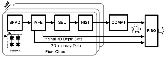
Figure 1.
The structure of the proposed SPAD sensor.
2.1. Multi-Mode Front End Circuit
In the SPAD sensor chip, the multi-mode front-end circuit is an important block for converting transient current pulses from a SPAD device into intensity data or time-of-flight data. Figure 2 depicts the circuit diagram of the MFE circuit, which encompasses four primary components: the quench circuit (QCH), the coincidence circuit, the TDC circuit, and the dual-mode output circuit (DMOUT). Upon receiving an avalanche current from the SPAD device, the quench circuit generates two types of pulses: CP [3:0] for counting purposes and TP [3:0] for timing measurements.
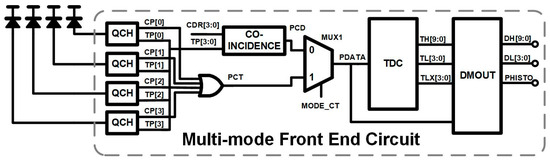
Figure 2.
The circuit diagram of the multi-mode front end circuit.
Due to the presence of abundant background light in the environment, a significant number of pulses received by the single-photon detector originate from background light rather than from the active emission of the laser. The coincidence circuit is used to detect whether multiple pulses arrive simultaneously from the four single-photon devices. If multiple pulses arrive at the same time, they are identified as signal pulses from the laser. If not, they are considered noise pulses caused by background light. The coincidence circuit filters the timing pulses TP [3:0] based on externally configured parameters, CDR [3:0], as threshold value to select those pulses that satisfy the coincidence criteria. It then outputs a pulse, PCD, for timing purposes. The intensity pulse chain, CP [3:0], is processed through a 4-input OR gate, generating a pulse, PCT, which serves as the trigger for counting operations.
The control signal, MODE_CT, dictates whether the MUX1 output, PDATA, is employed for timing or counting purposes. Specifically, when MODE_CT is set to 0, PDATA selects the pulse PCD for timing functions; conversely, when MODE_CT is set to 1, PDATA selects the pulse PCT for counting operations. In timing mode, upon receiving a PDATA pulse, the TDC initiates the timing sequence and latches the output data in dual-mode output circuit, which is then prepared for transmission once the detection duration is completed. In counting mode, the TDC’s internal ripple counter counts the number of pulses in PDATA pulse chains, and the dual-mode output circuit then sequentially outputs the counted data.
The single-photon devices in the chip are fabricated using the standard CMOS process, and their structure is shown in Figure 3. The depletion region of the single-photon device is formed by the PWell layer and the Deep NWell (DNW) layer. Compared with other CMOS SPAD structures, the SPAD device composed of PWell and Deep N-Well features a wider depletion region, higher quantum efficiency, and broader response wavelength. The PWell layer is biased through the P Plus (P+) layer, while the DNW layer is biased through the NWell layer and the N Plus (N+) layer. The doping concentration of the PWell layer decreases with depth, which effectively prevents edge breakdown effects. The DNW layers of all single-photon devices in the chip are interconnected through a metal layer, providing a voltage of 20 V with the breakdown field of about 5E5 V/cm. The P+ layer is connected to the quenching circuit. When a single-photon avalanche breakdown occurs, the avalanche current flows through the P+ layer into the quenching circuit.
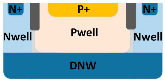
Figure 3.
The structural diagram of a CMOS single-photon avalanche device.
2.1.1. Quench Circuit
When a SPAD device triggers an avalanche, the current increases rapidly. The device will be damaged if it is allowed to continue to operate at a high current. Therefore, it is necessary to control the bias voltage of the device by a quench circuit to make it exit the avalanche state by reducing the bias of the device. Figure 4 illustrates the circuit diagram of the quench circuit. The input node connects to a SPAD device and receives the current emitted by the SPAD device. Upon the arrival of a photon, the device produces a substantial current, triggering the quench transistor, which is controlled by VQUENCH. This induced current causes the VSENSE voltage to increase, thereby reducing the bias voltage of the SPAD device and consequently diminishing the avalanche current. This process causes the single-photon device to exit the avalanche state. The voltage VSENSE, once it has traversed the threshold of a clamp transistor, is then fed into a D flip-flop as an analog pulse. This pulse causes the flip-flop to load the high voltage from input D to output Q. The duration of the high-level in the pulse output at Q is controlled by MODE_CT. When MODE_CT is set to 1, the circuit operates in photon counting mode. In this case, the high-level signal at Q is fed back to the reset pin of the DFF1 through the MUX2 input 1 after a 1 ns delay, pulling the Q’s high level down. Simultaneously, the voltage at Q outputs a 1 ns high-level CP pulse through the output MUX4 when Time_Gate is in a high-level state. When MODE_CT is set to 0, the circuit operates in time mode. The high-level signal at Q of DFF1 is fed back to the reset pin of the D flip-flop via MUX2 input 0 after passing through a pulse-width adjustment circuit, which pulls the high level down. At the same time, the voltage at Q outputs a widened high-level TP pulse through the output MUX3. The pulse-width adjustment circuit influences the duration time of high level by controlling the conduction state of a PMOS transistor with VWIDTH, thus regulating the charging speed of the PMOS in the inverter below it. A NMOS transistor is placed afterward to act as a charge capacitor, further delaying the charging process.
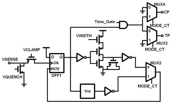
Figure 4.
The circuit diagram of the quench circuit.
2.1.2. Coincidence Circuit
Background light suppression is an important challenge in the design of single photon detector chips. This chip includes four SPAD devices in one pixel. The background light received by each SPAD is random in time, and there is a great probability that no two background light pulses will arrive at the same time, and the probability that three or four background light pulses will arrive at the same time is even lower. However, the laser pulses will reach these several neighboring devices at the same time. Therefore, it is possible to identify whether the current pulse is from the background light or the signal by detecting the number of pulses within a very short time window. The coincidence circuit is used to detect the number of pulses TP [3:0] triggered by the previous four quench circuits in a short period of time. This coincidence circuit adopts the circuit structure from H. Seo et al.’s work [8], which consists of 2-bit sorters, 2-input AND gates, and 4-input OR gates. Figure 5 shows the architecture of the coincidence circuit. This 2-bit sorter is composed of one 2-input AND gate and one 2-input OR gate, as shown in the dashed box on the left. Input signals are denoted as SA and SB and output signals are denoted as SC and SD. These outputs are designed to detect the co-occurrence of inputs. Table 1 shows the true table of this 2b sorter. SC is the result of SA OR SB and SD is the result of SA AND SB.
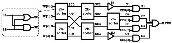
Figure 5.
The circuit diagram of the coincidence circuit.

Table 1.
True table of a 2-bit comparator.
A 4-bit sorter employs a cascade of two 2-bit sorters to detect the coincidence of four input time pulses which originated from the quench circuit, labeled as TP [0], TP [1], TP [2], and TP [3]. The first 2-bit sorter evaluates TP [0] and TP [1], yielding outputs SC0 and SD0, while the second sorter assesses TP [2] and TP [3], producing outputs SC1 and SD1. Each 2-bit sorter ascertains not only the presence of individual signals, but also the simultaneous activity of both inputs. Outputs SC0 and SC1 are then directed into a third 2-bit sorter, which evaluates the collective presence of the two signal pairs, resulting in outputs SC2 and SD2. Importantly, SC2, after being buffered by B1, emerges as O1, indicating whether any of the four signals are active. Furthermore, a fourth 2-bit sorter utilizes the outputs SD0 and SD1 from the initial two comparators to identify simultaneous activation among multiple input signals, yielding SC3 and SD3. Notably, SD3, after traversing buffer B2, transforms into O4, signifying the concurrent activation of all four signals. Lastly, a fifth 2-bit sorter refines the detection process, pinpointing whether two or three signals are concurrently present, with outputs O2 and O3 provided distinctly. CDR [0], CDR [1], CDR [2], and CDR [3] function as one-hot masking bits, enabling the selection of one result from O1, O2, O3, and O4 based on the programmed settings. When CDR [3:0] is set to ‘0001’, the threshold value is 0, and coincidence filtering is not applied. When CDR [3:0] is set to ‘0010’, the threshold value is 1. In this case, PCD will output a pulse only if two pulses occur simultaneously. When CDR [3:0] is set to ‘0100’, the threshold value is 2. In this case, PCD will output a pulse only if three pulses occur simultaneously.
2.1.3. TDC Circuit
The coincidence circuit is followed by the TDC circuit, which is used to convert the time pulses after coincidence detection into digital code values. Figure 6 illustrates the circuit diagram of the TDC circuit. This circuit receives pulses from the coincidence circuit for timing purpose or pulses from a 4-input OR gate in Figure 2 for counting purposes. Compared with shared TDC, such a dedicated TDC approach could record time values or counting values for all pixels at the expense of larger area. The TDC consists of four main components: a TDC gating generation circuit, a ring oscillator, four differential signal TDC registers, and a ripple counter. The TDC gating generation circuit is primarily responsible for producing the gating-enabled signal for the ring oscillator, enabling control over TDC operations in either synchronous or asynchronous time modes.
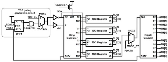
Figure 6.
The circuit diagram of the TDC circuit.
When the TDC is configured to operate in synchronous mode (TDCSYN = 1 and MODE_CT = 0), MUX5 is configured to choose the signal from MUX5’s input 1. The arrival of PDATA pulses triggers the DFF1. This flip-flop detects the rising edge and sets the Q output to a high level. The Q output, in conjunction with the STOP_PIXEL signal, passes through a 2-input AND gate to generate the gated signal for synchronous mode. In this setup, the falling edge of the synchronous gated signal is governed by STOP_PIXEL, while the rising edge is determined by PDATA. Ring oscillator starts operating when its inputs S and SX are 1 and 0, respectively. Eight outputs of the oscillator, T0, T0X, T1, T1X, T2, T2X, T3, and T3X, are connected to several differential registers to record the values in the oscillators. In this mode, MUX6 choose TLX [3] to trigger ripple counter. Moreover, the ripple counter outputs the counting number during the time period from the arrival of PDATA and the negative edge of STOPIXEL. In contrast, when the TDC operates in asynchronous mode (TDCSYN = 0 and MODE_CT = 0), MUX5 is configured to choose the signal from MUX5’s input 0. Both the rising and falling edges of the gated signal are controlled by TDC_EN. The TDC is in a constantly open state, ready to receive trigger pulses from the previous stage at any time. In this case, MUX6 still makes TLX [3] trigger the ripple counter, but the ripple counter keeps operating as long as TDC_EN is 1. The value at the moment PDATA arrives will be recorded by the dual mode output circuit introduced in Section 2.1.4. When the TDC is configured to operate in counting mode (MODE_CT = 1), MUX6 chooses PDATA directly to trigger the ripple counter to count the number of photon pulses. In this case, TDC gating the generation circuit, the ring oscillator, and differential signal TDC registers do not need to operate.
In either synchronous or asynchronous time modes, TDC’s ring oscillator provides timing pulses for the ripple counter. In this design, its frequency is controlled by the bias voltage VBTDCRO. Figure 7 illustrates the circuit diagram of the TDC’s ring oscillator. The TDC’s ring oscillator adopts the circuit structure from Robert K. Henderson et al.’s work [14], which is composed of eight inverter units. The circuit diagram of a single inverter unit is depicted in the dashed box on the left. Each inverter unit is controlled by input signals S and SX, which are used for gating. During the initialization of the circuit, S is set to 0 and SX to 1, ensuring that each inverter unit remains non-conductive. When RSTX is 0, the ring oscillator enters a reset state. In this state, T0, T1, T2, and T3 are set to 0, 1, 0, and 1, respectively, while T0X, T1X, T2X, and T3X are set to 1, 0, 1, and 0, respectively. When RSTX transitions to 1, the ring oscillator begins to enter a standby state. In this state, the NAND gates function as inverters, causing the output voltages of paired inverter units to be inverted relative to each other. When S is set to 1, SX is set to 0, and RSTX remains at 1, the inverter unit becomes conductive and the ring oscillator starts oscillating.
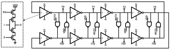
Figure 7.
The circuit diagram of the TDC’s ring oscillator.
In order to keep the load capacitance of the TDC output balanced, this chip uses a differential register to sample the output of the TDC. Figure 8a illustrates the circuit diagram of the TDC register. When RX is set to 0, the circuit enters a reset state, keeping both O+ and O− at a high level regardless of any oscillations in I+ and I−. When RX transitions to a high level, O+ and O− capture the states of I+ and I− at the exact moment of the RX rising edge. The latch structure of the top inverters ensures that the circuit maintains these output states until RX is pulled low again, which returns the circuit to the reset state.
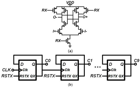
Figure 8.
The circuit diagrams of the TDC register (a) and the ripple counter (b).
The ring oscillator serves as the reference clock for the time-to-digital converter, with one of its outputs, TLX [3], routed to the ripple counter to function as the counting clock. Figure 8b shows the circuit diagram of the TDC ripple counter. The pulse source for the ripple counter is controlled by the signal MODE_CT as shown in Figure 6. When MODE_CT is set to 0, the signal TLX<3> is selected as the input pulse for time counting. Conversely, when MODE_CT is set to 1, the original pulse PDATA is chosen for photon counting. Within the circuit, the rising edge of pulses initiates binary counting in the first flip-flop. When the QX signal of this flip-flop transitions from 0 to 1, a carry signal is generated, which prompts the next flip-flop to begin counting in binary. This process facilitates the counting of 10-bit binary data.
2.1.4. Dual-Mode Output Circuit
To support data transmission in different detection modes, the chip is designed with a circuit that supports both synchronous and asynchronous outputs. Figure 9 illustrates the circuit diagram of the dual-mode output circuit, which supports two data output modes: synchronous and asynchronous. In synchronous mode and counting mode, when TDCSYN is set to 1, the data path follows the blue line depicted in the Figure 9. In this mode, the external input signal TRIGSYN triggers 14 parallel flip-flops to load the TDC input data, including TH [9:0] and TL [3:0]. Additionally, the TRIGSYN signal generates a PHISTO pulse for the histogram block after a 2 ns delay. This delay is introduced to account for the long data path from the TDC to the histogram block, where data are loaded into the D flip-flops and selected through the SEL block. In addition, in counting mode, only TH [9:0] are valid data for counting purposes.
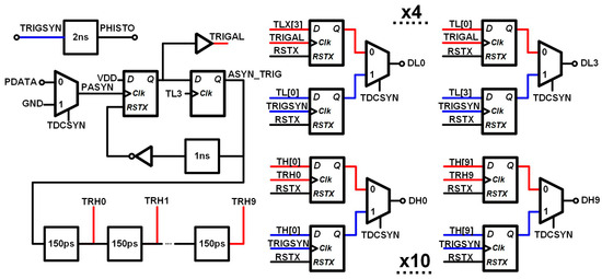
Figure 9.
The circuit diagram of the dual-mode output circuit. Red line: asynchronous readout mode. Blue line: synchronous readout mode.
In asynchronous mode, when TDCSYN is set to 0, the data path follows the red line shown in the Figure 9. The trigger signal for the D flip-flops is generated by PDATA. Upon the arrival of PDATA, the first register in the trigger path loads a high level, generating the TRIGAL signal. This signal samples the output state of the TDC ring oscillator at that moment. Since this signal is not in the same clock domain as the TDC ripple counter, it must be further sampled by the TL [3] signal to generate the ASYN_TRIG signal. The ASYN_TRIG signal, now synchronized with the ripple counter’s clock domain, samples the TDC ripple counter sequentially from the least significant bit (LSB) to the most significant bit (MSB). Given that the signal propagation time for one bit in the ripple counter is approximately 150 ps, a 150 ps delay is introduced to ensure proper sampling. After sampling each bit, the process waits for 150 ps before proceeding to the next bit, continuing until the TH9 data are fully sampled. Once TRH9 is generated, all TDC data are recorded in the D flip-flops.
2.2. SEL Circuit
In synchronous mode, the signals DH [9:0] and DL [3:0] from the dual-mode output circuit are first selected by the SEL circuit before being forwarded to the histogram circuit. The SEL logic decodes the lower 4 bits of TDC using a 4-3 decoder, as illustrated in Figure 10. In this context, the lower 4 bits are referred to as DL [3:0], while the upper 10 bits are denoted as DH [9:0]. The truth table for the 4-3 decoder is presented in Table 2. The output signal from the 4-3 decoder is labeled as DL_DEC [2:0]. DH and DL_DEC serve as inputs to the MODE_SEL logic. Due to limited on-chip storage space, only 7 bits can be selected from the 13 bits to be sent to the subsequent histogram module. The PHISTO is further delayed by an additional 2 ns to ensure that the data are fully established on the data line by the time the rising edge of the PHISTO occurs.
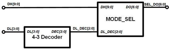
Figure 10.
The block diagram of the SEL circuit.
Table 2.
The truth table of the 4-3 decoder.
2.3. Histogram Circuit
In synchronous mode, SEL_DO [6:0] from the SEL circuit is sent to the histogram circuit to specify the address for PHISTO. Figure 11 illustrates the diagram of the histogram circuit, which is designed to generate statistics histograms of the photon time of flight and provides the capability to output the values of each bin. The histogram circuit comprises an address decoder circuit and 128 groups of 8-bit binary counters. The address decoder is used to convert the 7-bit TDC time data output from the SEL block into a 128-bit address ADDR [127:0] with one-hot code. This address data are utilized to identify the corresponding counter from the 128 counters. To save storage resources, a new type of histogram counting circuit has been designed, which supports both pulse counting and data shifting for computation.
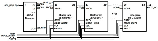
Figure 11.
The diagram of the histogram circuit.
As shown in Figure 12, in statistical counting mode (MODE_HISTO = 0), the binary counters start receiving pulses for cumulative counting. When some bit in the 128-bit address ADDR [127:0] is 1, the corresponding counter is selected and the counter value is incremented when the pulse in PHISTO occurs. In data shifting output mode (MODE_HISTO = 1), the binary counters cease to receive input pulses and instead shift data horizontally under the control of the CLK signal. This allows each bin’s data to be output sequentially through the external data port.
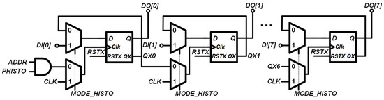
Figure 12.
The circuit diagram of the histogram counter unit.
The histogram circuit initially operates in statistical counting mode, where it completes the counting of all time data before transitioning to data shifting mode. In data shifting mode, the counting results from the 128 time bins are transferred to the on-chip computation circuit. As the data are input into the computation circuit sequentially according to the time bins, there is no need for additional large storage space. Instead, the computation circuit can process the data directly in a pipelined fashion. The computation circuit supports multiple calculation methods, including identifying the maximum peak and determining the position of the centroid near the peak, which are described in Algorithm 1 and Algorithm 2, respectively. It should be noted that IRF, mentioned in Algorithm 2, stands for the Instrumental Response Function of this chip.
| Algorithm 1 Identifying the maximum peak | |
| Input: Histogram array H = h (0), h (1), …, h (127); | |
| Output: peak value M, peak position P; | |
| i is the internal temporary variable; | |
| 1 | set i = 0, P = 0, M = 0; |
| 2 | while i < 128 do |
| 3 | if h (i) > M then |
| 4 | P = i, M = h (i); |
| 5 | end |
| 6 | i = i + 1; |
| 7 | end |
| Algorithm 2 Determining the position of the centroid near the peak | |
| Input: Histogram array H = h (0), h (1), …, h (127), IRF width W, peak position P; | |
| Output: position of the centroid C; | |
| Rmin and Rmax are internal variables, which denote the infimum and supremum of valid data range for centroid; h_weight denotes the accumulation of array data in valid range; p_sum denotes the accumulation of weighted position values; i is the internal temporary variable; | |
| 1 | set Rmin = P − W/2, Rmax = Rmin + W − 1, h_weight = 0, p_sum = 0, i = 0; |
| 2 | while i < Rmin do |
| 3 | i = i + 1; |
| 4 | end |
| 5 | while i ≤ Rmax do |
| 6 | h_weight = h_weight + h (i); |
| 7 | p_sum = p_sum + h (i) × i; |
| 8 | i = i + 1; |
| 9 | end |
| 10 | C = p_sum/h_weight; |
2.4. PISO Circuit
Figure 13 shows the circuit diagram of PISO circuit. This circuit operates in two modes: data loading mode and serial output mode. In data loading mode (MODE_PISO = 0), the module receives output data from the MFE or histogram block, with its internal register data values updating according to changes in the output. In serial output mode (MODE_PISO = 1), the data are transferred serially across the PISO unit, sequentially outputting the data values for all 64 pixels.
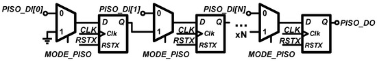
Figure 13.
The circuit diagram of the PISO circuit.
3. Experimental Results
The proposed SPAD sensor was fabricated using a 0.13 µm mixed-signal CMOS process, with a chip size of 2.8 × 5 mm2. Its power consumption is approximately 12.9 mW. Figure 14 presents a microphotograph of the sensor design, with labeled functional areas. The top two rows of the chip consist of a 64 × 1 SPAD array, the MFE block, and the SEL block, while the rectangular area in the middle is dedicated to the histogram block. To test the chip, we constructed a system comprising an FPGA development board, a laser source, and optical lenses, as shown in Figure 15a. The measurement experiment utilized a laser with a continuous-spectrum light source, whose spectral range extends from 430 nm to 2400 nm, covering the spectral response range of the single-photon detector. The laser supports external triggering with a trigger frequency set at 50 kHz. In this experiment, a control circuit was used to synchronize the operation cycles of both the laser and the detector. Figure 15b illustrates the illuminated object and the background white board. The chip was bonded to the PCB board. The operating voltages for each subcircuit mentioned above are routed to the PCB’s SMB interfaces, which are connected to an external power supply. We employed an FPGA to provide signal timing to control its working mode. Since the operating voltage of the proposed chip differs from that of the FPGA, we used several level shifter circuits on the PCB to convert signals between different voltage domains. The FPGA connects to the PCB via an FMC interface. Figure 16 illustrates the structure of the test system. We utilized an embedded system on the FPGA, where the host interacts with the FPGA’s programmable logic through software code. The programmable logic consists of the following main modules: the STG (Signal Timing Generation) Module, the Reg_Config (Register Configuration) Module, and the D_Storage (Data Storage) Module. The STG Module provides the necessary timing signals for the sensor, enabling it to trigger laser emission and ensure proper operation of the detector in test, counting, and timing modes. The Reg_Config Module employs a PISO structure, converting parallel data inputs into a serial format for input to the chip. The D_Storage Module stores data output from the dual-mode output circuit, as described in Section 2.1.4.
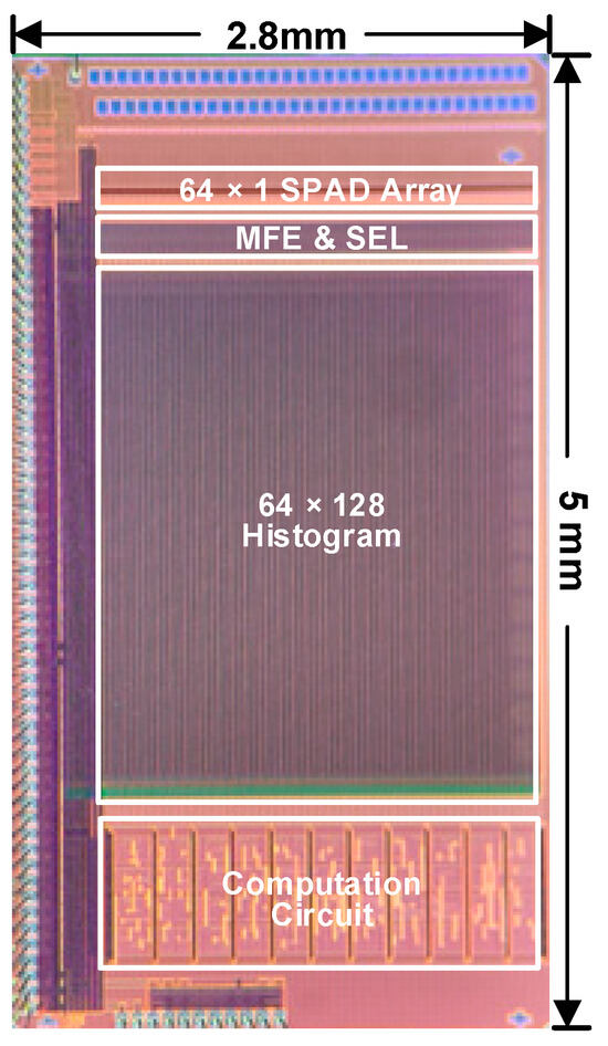
Figure 14.
Micrograph of the proposed chip.
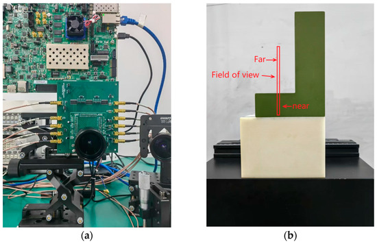
Figure 15.
A photograph of the test system, including the FPGA, optical lens, and laser (a), and the illuminated object (b).
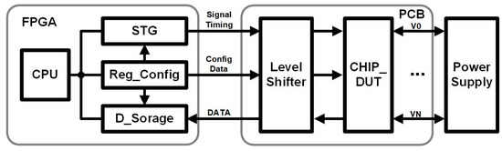
Figure 16.
The structure of the test system.
Figure 17a depicts the measurement results of 64-pixel output data with different photon pulse times. The lines from top line to bottom line approximately represent the measurement results from pixel 0 to pixel 63. The output code values of the pixels exhibit a strong linear relationship with the pulse time-of-flight. Under the same photon pulse, the output values of all pixels should be identical. However, due to process variations, the oscillation periods of the ROs in the TDC are inconsistent, resulting in discrepancies in the output curves of different pixels. Based on these test curves, we extracted the slope and intercept and calculated the calibration coefficients by comparing them with average values. By applying them to calibrate the output data for each pixel, the peak-to-peak deviation between pixels has been reduced from 449 LSB to 18.3 LSB. Figure 17b depicts the measurement results of 64 pixels when breakdown pulses are triggered at 400 ns in Figure 17a. The output of each pixel maintains a very good linear relationship with time. Based on the relationship between the output code value and time, it can be calculated that the average LSB corresponding to the time resolution is 131.85 ps.
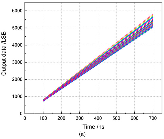
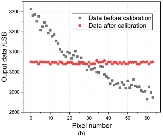
Figure 17.
The measurement results of the output data versus trigger time in 64 pixels (a) and the comparison results of the output results from the 64 pixels triggered at 400 ns before and after calibration (b).
Figure 18 illustrates the suppression of the pile-up effect by the coincidence circuit. The x-axis is divided into 64 intervals, ranging from 0 to 8192 and y-axis is the statistical result of the TDC timing values falling within each interval during testing period. The distance between the optical lens and the background white board shown in Figure 15b is 1.5 m and the intensity of the background light is 6k lux. During the testing process, the pulse energy of the laser was approximately 0.1 µJ. As the coincidence threshold increases from 0 to 1, the pile-up effect is completely eliminated. The background data at the maximum point are suppressed by 95.4%, with an average suppression of 86%. As the coincidence threshold increases to 2, the noise is observed to decrease significantly. However, as the coincidence threshold increases, the amplitude of the signal also decreases. Therefore, it is not always better to have a higher coincidence threshold. Instead, an appropriate threshold should be chosen based on the actual intensity of the background light and the signal-to-noise ratio. An appropriate threshold could precisely suppress the pile-up effect and maintain a good signal-to-noise ratio. Under the condition of laser pulse energy of 0.1 µJ and a 6k lux background, it is appropriate to set the coincidence detection threshold to 1. When the threshold is set to 2, some signal information may also be suppressed. It should be noted that since this chip starts timing after receiving a breakdown pulse, the peak of pile-up occurs at the tail of the histogram.
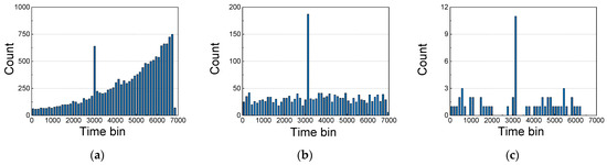
Figure 18.
Histograms generated under different coincidence detection threshold values: threshold value = 0 (a), threshold value = 1 (b), and threshold value = 2 (c).
Figure 19 illustrates the impact of laser power on the generated histogram. It can be observed that as the laser power increases, the peak height of the histogram becomes higher, and the relative level of noise interference decreases.
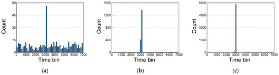
Figure 19.
Histograms generated under different laser illumination intensities: small laser power (a), moderate laser power (b), and strong laser power (c).
Figure 20 presents the distance measurement results of a 64-pixel single-photon detector. Its field of view is indicated by the red area in Figure 15b. Because this chip starts timing after receiving a breakdown pulse, bigger data represent a smaller distance. We can find an output data transition from 2855 to 2903, which means this chip detects the distance difference in its linear field of view. After the test data have been corrected, it is evident that the distance measurement results show relatively good uniformity. Table 3 lists the design parameters and test results of this SPAD detector chip.
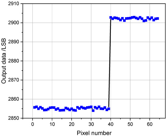
Figure 20.
Depth measurement results of the SPAD sensor chip with the field of view depicted in Figure 15b.
Table 3 shows the parameter items of the proposed SPAD chip and related works. Compared to the work of Alfonso Incoronato et al. [18], more detection modes are realized, including 2D intensity detection, 3D synchronous detection, and 3D asynchronous detection. In addition, TDC circuit and on-chip histogram circuit are also realized in the proposed chip. Compared to the work of Federica Villa et al. [19], the proposed chip has higher TDC resolution and lower dark count rate. Compared to the work of Xiangshun Kong et al. [20], the proposed chip not only supports photon-counting mode, but could also work in synchronous mode and asynchronous mode.
Table 3.
Parameter items of the proposed SPAD chip sensor and related works.
Table 3.
Parameter items of the proposed SPAD chip sensor and related works.
| Items | This Work | Alfonso Incoronato et al. [18] | Federica Villa et al. [19] | Xiangshun Kong et al. [20] |
|---|---|---|---|---|
| Sensor type | SPAD | SPAD | SPAD | SPAD |
| Detection mode | 2D intensity/ 3D image (synchronous and asynchronous) | Single-Hit/ Multi-Hit | Photon-counting/ global-shutter | Photon-counting |
| Technology | 0.13 μm | 160 nm BCD | 0.35 μm | 0.18 μm |
| Pixel format | 64 × 1 | 32 × 1 | 60 × 1 | 256 × 2 |
| Pixel pitch | 35 μm | 125 μm | 150 μm | 15 μm |
| Chip size | 2.8 × 5 mm2 | 2.215 × 4.92 mm2 | 2 × 9.3 mm2 | - |
| Excess voltage | 1.2 V | - | 5 V | 1.8 V |
| Power consumption | 12.9 mW | - | - | - |
| TDC resolution | 132 ps | N.A. | 250 ps | N.A. |
| TDC depth | 13 | N.A. | 10 | N.A. |
| On-chip histogram | 8b × 128 | N.A. | N.A. | N.A. |
| Dark count rate (DCR) | 950 | - | 2.5k | <1000 |
| PDE | 8.4% | 65% | 50% | - |
4. Conclusions
In this paper, a 64-pixel single-photon detector chip with an on-chip histogram has been developed. This chip possesses multi-mode detection capabilities, including 2D intensity detection, 3D synchronous detection, and 3D asynchronous detection. Benefiting from the reuse of storage and data shifting circuit structures, the chip saves the area required for the histogram. The chip was fabricated using a 0.13 μm CMOS process. Measurement results indicate that as the threshold increases, the coincidence circuit can effectively suppress background light. We constructed an experimental setup to test the chip’s distance detection capabilities. The test data, after correction, demonstrate that the chip exhibits good detection performance. Currently, linear-array LiDAR has been widely applied in fields such as autonomous driving. Single-photon avalanche detectors with ultra-high gain are expected to further enhance the spatial resolution and measurement range of LiDAR. Moreover, the integration of 2D intensity imaging and 3D range imaging has become an important development trend. This chip supports multiple imaging modes and, compared to traditional architectures, offers advantages such as a shared optical path, enabling pixel-level fusion. It is expected to facilitate tasks such as higher accuracy and higher frame-rate target recognition, thereby paving the way for large-scale 3D imaging and high-level imaging tasks.
Author Contributions
Conceptualization, Z.H.; methodology, H.L., J.W. and B.C.; validation, H.L.; writing—original draft preparation, H.L.; writing—review and editing, H.L. and Z.H.; project administration, Z.H.; funding acquisition, Z.H. All authors have read and agreed to the published version of the manuscript.
Funding
This work was supported in part by the National Natural Science Foundation of China, under Grants 62235009 and 62374039, and in part by the National Key Research and Development Program of China, under Grant 2021YFA1200700.
Data Availability Statement
Data are included in the article.
Conflicts of Interest
The authors declare no conflict of interest.
References
- Xia, F.; Campi, F.; Bahreyni, B. Tri-Mode Capacitive Proximity Detection Towards Improved Safety in Industrial Robotics. IEEE Sens. J. 2018, 18, 5058–5066. [Google Scholar] [CrossRef]
- Scott, R.; Jiang, W.; Deen, M.J. CMOS Time-to-Digital Converters for Biomedical Imaging Applications. IEEE Rev. Biomed. Eng. 2023, 16, 627–652. [Google Scholar] [CrossRef] [PubMed]
- Qian, R.; Lai, X.; Li, X. 3D Object Detection for Autonomous Driving: A Survey. Pattern Recognit. 2022, 130, 108796. [Google Scholar] [CrossRef]
- Xu, S.; Yu, H.; Wang, H.; Chai, H.; Ma, M.; Chen, H.; Zheng, W.X. Simultaneous Diagnosis of Open-Switch and Current Sensor Faults of Inverters in IM Drives Through Reduced-Order Interval Observer. IEEE Trans. Ind. Electron. 2024, 1–12. [Google Scholar] [CrossRef]
- Poisson, V.; Guicquero, W.; Sicard, G. Luminance-Depth Reconstruction From Compressed Time-of-Flight Histograms. IEEE Trans. Comput. Imaging 2022, 8, 148–161. [Google Scholar] [CrossRef]
- Niclass, C.; Soga, M.; Kato, S. A 0.18 μm CMOS single-photon sensor for coaxial laser rangefinders. In Proceedings of the 2010 IEEE Asian Solid-State Circuits Conference, Beijing, China, 8–10 November 2010; pp. 1–4. [Google Scholar]
- Cristiano, N.; Mineki, S.; Hiroyuki, M.; Satoru, K.; Manabu, K. A 100-m Range 10-Frame/s 340 × 96-Pixel Time-of-Flight Depth Sensor in 0.18-μm CMOS. IEEE J. Solid-State Circuits 2013, 48, 559–572. [Google Scholar]
- Seo, H.; Kim, B.; Chun, J.H.; Kim, S.J.; Choi, J. CMOS depth sensor with programmable filter circuits for environment-adaptive noise suppression. Electron. Lett. 2018, 54, 1122–1124. [Google Scholar] [CrossRef]
- Ota, Y.; Morimoto, K.; Sasago, T.; Shinohara, M.; Kuroda, Y.; Endo, W.; Maehashi, Y.; Maekawa, S.; Tsuchiya, H.; Abdelahafar, A.; et al. A 0.37W 143dB-Dynamic-Range 1Mpixel Backside-Illuminated Charge-Focusing SPAD Image Sensor with Pixel-Wise Exposure Control and Adaptive Clocked Recharging. In Proceedings of the 2022 IEEE International Solid-State Circuits Conference (ISSCC), San Francisco, CA, USA, 20–26 February 2022; pp. 94–96. [Google Scholar]
- Manuzzato, E.; Tontini, A.; Seljak, A.; Perenzoni, M. A 64 × 64-Pixel Flash LiDAR SPAD Imager with Distributed Pixel-to-Pixel Correlation for Background Rejection, Tunable Automatic Pixel Sensitivity and First-Last Event Detection Strategies for Space Applications. In Proceedings of the 2022 IEEE International Solid-State Circuits Conference (ISSCC), San Francisco, CA, USA, 20–26 February 2022; pp. 96–98. [Google Scholar]
- Wang, J.; Huang, Z.; Chen, B.; Shang, H.; Zheng, J.; Lv, H.; Chen, C.; Liu, Q.; Liu, M. A 32 × 32 Flash LiDAR SPAD Sensor with Up-to-1kfps Motional Target Detection by Threshold-adaptive 2D Dynamic Vision. In Proceedings of the 2024 IEEE Custom Integrated Circuits Conference (CICC), Denver, CO, USA, 21–24 April 2024. [Google Scholar]
- Niclass, C.; Favi, C.; Kluter, T.; Gersbach, M.; Charbon, E. A 128 × 128 Single-Photon Image Sensor With Column-Level 10-Bit Time-to-Digital Converter Array. IEEE J. Solid-State Circuits 2008, 43, 2977–2989. [Google Scholar] [CrossRef]
- Pavia, J.M.; Scandini, M.; Lindner, S.; Wolf, M.; Charbon, E. A 1 × 400 Backside-Illuminated SPAD Sensor With 49.7 ps Resolution, 30 pJ/Sample TDCs Fabricated in 3D CMOS Technology for Near-Infrared Optical Tomography. IEEE J. Solid-State Circuits 2015, 50, 2406–2418. [Google Scholar] [CrossRef]
- Henderson, R.K.; Johnston, N.; Della Rocca, F.M.; Chen, H.; Li, D.D.U.; Hungerford, G.; Hirsch, R.; Mcloskey, D.; Yip, P.; Birch, D.J. A 192 × 128 Time Correlated SPAD Image Sensor in 40-nm CMOS Technology. IEEE J. Solid-State Circuits 2019, 54, 1907–1916. [Google Scholar] [CrossRef]
- Niclass, C.; Soga, M.; Matsubara, H.; Ogawa, M.; Kagami, M. A 0.18-μm CMOS SoC for a 100-m-Range 10-Frame/s 200 × 96-Pixel Time-of-Flight Depth Sensor. IEEE J. Solid-State Circuits 2014, 49, 315–330. [Google Scholar] [CrossRef]
- Zhang, C.; Lindner, S.; Antolović, I.M.; Pavia, J.M.; Wolf, M.; Charbon, E. A 30-frames/s, 252 × 144 SPAD Flash LiDAR With 1728 Dual-Clock 48.8-ps TDCs, and Pixel-Wise Integrated Histogramming. IEEE J. Solid-State Circuits 2019, 54, 1137–1151. [Google Scholar] [CrossRef]
- Gyongy, I.; Erdogan, A.; Dutton, N.; Mai, H.; Della Rocca, F.M.; Henderson, R.K. A 200kFPS, 256 × 128 SPAD dToF sensor with peak tracking and smart readout. In Proceedings of the International Image Sensor Workshop, Online, 20–23 September 2021. [Google Scholar]
- Incoronato, A.; Severini, F.; Madonini, F.; Villa, F.; Zappa, F. Linear SPAD array for quantum communication. In Proceedings of the SPIE 11771, Quantum Optics and Photon Counting 2021, Online, 18 April 2021; Volume 117710A. [Google Scholar]
- Villa, F.; Lussana, R.; Tamborini, D.; Tosi, A.; Zappa, F. High-Fill-Factor 60 × 1 SPAD Array With 60 Subnanosecond Integrated TDCs. IEEE Photonics Technol. Lett. 2015, 27, 1261–1264. [Google Scholar] [CrossRef]
- Kong, X.; Bu, X.; Mao, C.; Zhang, L.; Ma, H.; Yan, F. SPAD Sensors with 256 × 2 Linear Array for Time Delay Integration Demonstration. In Proceedings of the 2018 IEEE SENSORS, New Delhi, India, 28–31 October 2018; pp. 1–5. [Google Scholar]
Disclaimer/Publisher’s Note: The statements, opinions and data contained in all publications are solely those of the individual author(s) and contributor(s) and not of MDPI and/or the editor(s). MDPI and/or the editor(s) disclaim responsibility for any injury to people or property resulting from any ideas, methods, instructions or products referred to in the content. |
© 2025 by the authors. Licensee MDPI, Basel, Switzerland. This article is an open access article distributed under the terms and conditions of the Creative Commons Attribution (CC BY) license (https://creativecommons.org/licenses/by/4.0/).