Article

Overcoming Printed Circuit Board Limitations in an Energy Harvester with Amplitude Shift Keying and Pulse Width Modulation Communication Decoder Using Practical Design Solutions

by
Mohamad Al Sabbagh
1,*,
Rony E. Amaya
2,*,
Mustapha Chérif-Eddine Yagoub
1 and
Abdullah M. Almohaimeed
3
1
School of Electrical Engineering and Computer Science, University of Ottawa, Ottawa, ON K1N 6N5, Canada
2
Department of Electronics, Carleton University, Ottawa, ON K1S 5B6, Canada
3
Department of Electrical Engineering, College of Engineering, Qassim University, Buraydah 51452, Saudi Arabia
*
Authors to whom correspondence should be addressed.
Electronics 2025, 14(3), 485; https://doi.org/10.3390/electronics14030485
Submission received: 9 December 2024 / Revised: 12 January 2025 / Accepted: 16 January 2025 / Published: 25 January 2025

Abstract

:
This paper presents PCB design solutions for implementing a radiative-field RF energy harvester with an ASK-PWM decoding communication scheme using available commercial components. The paper provides the design approach and tackles key challenges such as the impact of inductive parasitic effects at the output of the harvester, how to maintain the P C E at a constant value regardless of the time constant at the output of the communication path’s rectifier, and the difficulty of changing the aspect ratio of the discrete inverter used for PWM decoding. These challenges are addressed by using multiple capacitors connected in parallel at the output of the rectifier to reduce inductive parasitic effects, adding a series resistor in the communication path’s rectifier to isolate its loading from impacting the P C E , and utilizing a potentiometer in the inverter to realize PWM decoding on PCB. The system was manufactured using FR-4 substrate material with a size of 5 cm × 4 cm × 0.6 cm, harvesting energy at the ISM frequency of 924 MHz with a P C E of 42.12 % at a bit rate of 15 Kbps. Moreover, the system consumes only 355 μW of power and maintains correct harvesting and decoding operation in the antenna separation range of 6–12 cm. This work aims to provide an alternative to IC realization by implementing the system entirely using commercial discrete components, reducing costs, adding flexibility, reducing development time, and allowing for simple debugging.

1. Introduction

Simultaneous Wireless Information and Power Transfer (SWIPT) has attracted a plethora of attention in the recent literature as a mechanism used for powering up and communicating with standalone devices such as Internet-of-Things (IoT), biomedical implants, electric vehicles, and underwater applications [1,2,3,4,5,6]. This concept brings about removing power and data wired connectivity, improving flexibility, and removing the need for batteries for the system. SWIPT is based on the combination of two technologies. The first is Wireless Power Transfer (WPT), which transfers RF power wirelessly from a dedicated source or ambience to the receiver, from which the RF power is converted to DC to power up said receiver. This power transfer can be performed in the near field using inductive links or radiative fields using antennas. The second is Wireless Information Transfer (WIT), which is based on the modulation and demodulation of the RF signal to transfer data wirelessly. This combination can be in a separate-channel scheme where the power and data are orthogonal to each other, which would make them unimpacted by one another at the expense of increased area of implementation, or it can be in a shared-channel scheme, which improves compactness at the cost of performance reduction [2,3].
Communication schemes can be categorized in a shared-channel SWIPT system as single modulation or double modulation. Amplitude Shift Keying (ASK), On–Off Keying (OOK), Frequency Shift Keying (FSK), and Phase Shift Keying (PSK) are all examples of single modulation category. In ASK, the modulating carrier is shifted high and low according to the data bits at the input of the modulator. This modulated signal can be demodulated in a coherent (synchronous) way using clock-generating circuitry and a Phase-Locked Loop (PLL) at the receiver side or in a noncoherent (asynchronous) way using an envelope detector, which removes the need for the clock generation and PLL circuitries [7]. Noncoherent ASK in SWIPT brings the advantages of low complexity, low power consumption, and the removal of phase detection. However, the disadvantages are impacted performance due to the continuously varying power envelope of the RF power, which would impact the power transfer efficiency and low data rate compared to FSK and PSK [8]. OOK is similar to ASK but with a modulation index of 100%. This scheme simplifies the receiver structure even more compared to ASK due to the wide range between bits “1” and “0”, but for WPT purposes, it is inefficient since during data transmission of bit “0”, power is discontinued from the receiver. FSK and PSK are based on digitally changing the frequency and phase of the modulating signal to change the data bits. Both FSK and PSK require phase detection and clock-generating circuitries, which would increase the power consumption, area utilization, and receiver complexity. Also, FSK and PSK are usually incorporated with Gaussian filtering and differential signaling, respectively, adding to the receiver’s complexity, area utilization, and power consumption [9]. FSK and PSK have high data rates and constant power envelope advantages, whereas the latter advantage is suitable for WPT. However, the cons of FSK and PSK outweigh the pros in terms of WPT performance.
Instead of a single modulation scheme, a double modulation scheme can be used to gain more advantages, such as asynchronous clock extraction and improved receiver functionality [10]. This led to an emerging double-modulation scheme in the recent literature used heavily in short-range SWIPT systems for biomedical applications: Amplitude Shift Keying with Pulse Width Modulation (ASK-PWM). Instead of using ASK for data decoding, the ASK signal is demodulated to extract the asynchronous clock from the ASK-PWM signal. At the same time, the PWM is decoded to extract the data based on the digital pulse width of the decoded ASK signal. ASK-PWM maintains the advantages of noncoherent ASK demodulation regarding receiver complexity, area reduction, and power consumption. Also, when limiting the ASK modulation index within 5–10% of the RF power envelope, the RF power envelope will not change drastically in a way that would impact power efficiency and would also maintain a good room for demodulating the ASK signal, reducing the Bit Error Rate (BER) [11].
Earlier work in the literature has utilized ASK-PWM SWIPT, primarily focusing on Integrated Circuit (IC) implementation for biomedical applications. In [11], an 11 μW transceiver was presented for powering and communicating with implantable devices. The IC was fabricated using a 65 nm process and utilized ASK-PWM at a reconfigurable data rate between 4 and 20 Mbps; it also used an off-chip antenna at the frequency of 1.32 GHz at a separation of 3.5 cm from a 125 mW transmitting antenna. In [12], a 13.56 MHz inductively coupled WPT system was presented. It used a hybrid organic/metal oxide process to achieve a bit rate of 75 bits/s using ASK-PWM with a size of 11 × 11 cm for organic applications. A 4.5 μW 3-channel wireless intra-cardiac acquisition system was presented in [13]. The system was implemented using a 180 nm process, inductively coupled WPT at 13.56 MHz with a data rate of 88.3 Kbps. In [14], an implantable device capable of locomotion in a fluid medium was implemented using a 65 nm process. It received 500 μW power from a 2 W source at a frequency of 1.86 GHz with a separation distance of 5 cm at a data rate of 2.5–25 Mbps using ASK-PWM. A Silicon-on-Chip (SoC) WPT using magnetic induction with ASK-PWM scheme for the flexible dithering feature is presented in [15]. They used a 180 nm process to implement the system with a power consumption of 50 mW. In [16], a comparator-less ASK-PWM design for inductive coupling WPT was implemented. It used a frequency divider, frequency multiplier, and data sampler for clock and data recovery of ASK-PWM realized using a 180 nm process at a data rate of 2 Mbps. A cochlear implant system for stimulation using an 8-channel inductive link with ASK-PWM was presented in [17]. A custom chip was designed for the receiver part with a data rate of 120 Kbps at a total current consumption of 105 mA. A 900 MHz, inductively coupled ASK-PWM system with a 10 Mbps data rate is presented for brain implant purposes [18]. The system was composed of 32 ICs manufactured using a 65 nm process. A 180 nm SoC near field resonant inductive link with ASK-PWM at 40.68 MHz is presented in [19]. The system enabled up to 16 implantable stimulators at an 8 cm separation with a data rate of 10 Kbps, consuming 27 μW of power from a 2 W transmitter.
As seen from the state-of-the-art review, the focus was mainly on implementing an inductively coupled ASK-PWM WPT system implemented on an IC for biomedical applications. Although IC realization brings the advantages of miniaturization and high integration, it increases complexity, costs, inflexibility, and development time. For example, producing a PCB prototype typically requires 2–3 weeks, whereas an IC prototype takes 24–48 weeks. These disadvantages can be avoided by implementing the system entirely on PCB using commercially available discrete components. As of this date, no work has been conducted to achieve such an option. The state-of-the-art did not present a detailed design approach for the energy harvester with an ASK-PWM decoder.
Three challenges were faced when attempting to realize this system in a discrete fashion. The first was the parasitic inductor that existed at the output of the rectifier’s filter, which caused the RF to leak into the output regardless of the rectification capacitor’s value. The second challenge is that the Power Conversion Efficiency ( P C E ) value was impacted by the load resistance value at the output of the communication rectifier, which reduced the flexibility in changing the time constant of the communication filter. The last challenge was the inflexibility of changing the aspect ratio of the inverter’s discrete P-Field Effect Transistor (P-FET) in the PWM decoder to achieve the skewing operation necessary for successful data decoding. The first two solutions improve the performance of the discrete implementation, while the third one is critical to realize the system in a discrete fashion.
In this work, we implemented a fully discrete ASK-PWM energy harvesting system using commercially available components. The PCB is an FR-4 substrate of size 5 cm × 4 cm × 0.6 cm and harvests energy at the 924 MHz ISM frequency, while the ASK-PWM bit rate is at 15 Kbps. The contributions are highlighted in the complete discrete implementation of the system on PCB, its detailed design approach, and the solutions to the challenges exhibited in implementing such a system in a discrete format. These solutions and improvements are described as follows:
  • The impact of the inductive parasitic effects was solved by splitting the big rectification capacitor at the output of the rectification filter into multiple smaller capacitors. This reduced the inductive contribution to a large extent, leading to a smoother DC output;
  • A lossy resistor was added in series with the communication’s path rectifier to drop the amount of current in this path to a minimal value. This allowed the P C E of the harvester’s path to remain at an almost constant value regardless of changes in the load value of the communication rectifier, adding flexibility in tuning the time constant of the communication filter;
  • The aspect ratio inflexibility for the skewing operation was solved by adding a potentiometer between the P-FET drain terminal and the inverter output. The potentiometer controls and increases the time constant to achieve and set the correct level of the skewing operation.
Furthermore, commercial antennas were used to harvest radiative energy so that more applications can be targeted using this system other than biomedical applications, such as beamforming control systems, Wireless Sensor Networks (WSNs) powering, and wireless actuator control. The system was tested with an antenna separation distance of 6–12 cm.
The paper is structured as follows: Section 2 is the proposed circuit structure, and Section 3 contains the design approach split into four phases, including the proposed solutions and improvements. Section 4 presents the complete system’s PCB and its measurements under radiative-field operation for validating harvesting, data, and clock recovery. Section 5 is the conclusion.

2. Proposed Circuit Structure

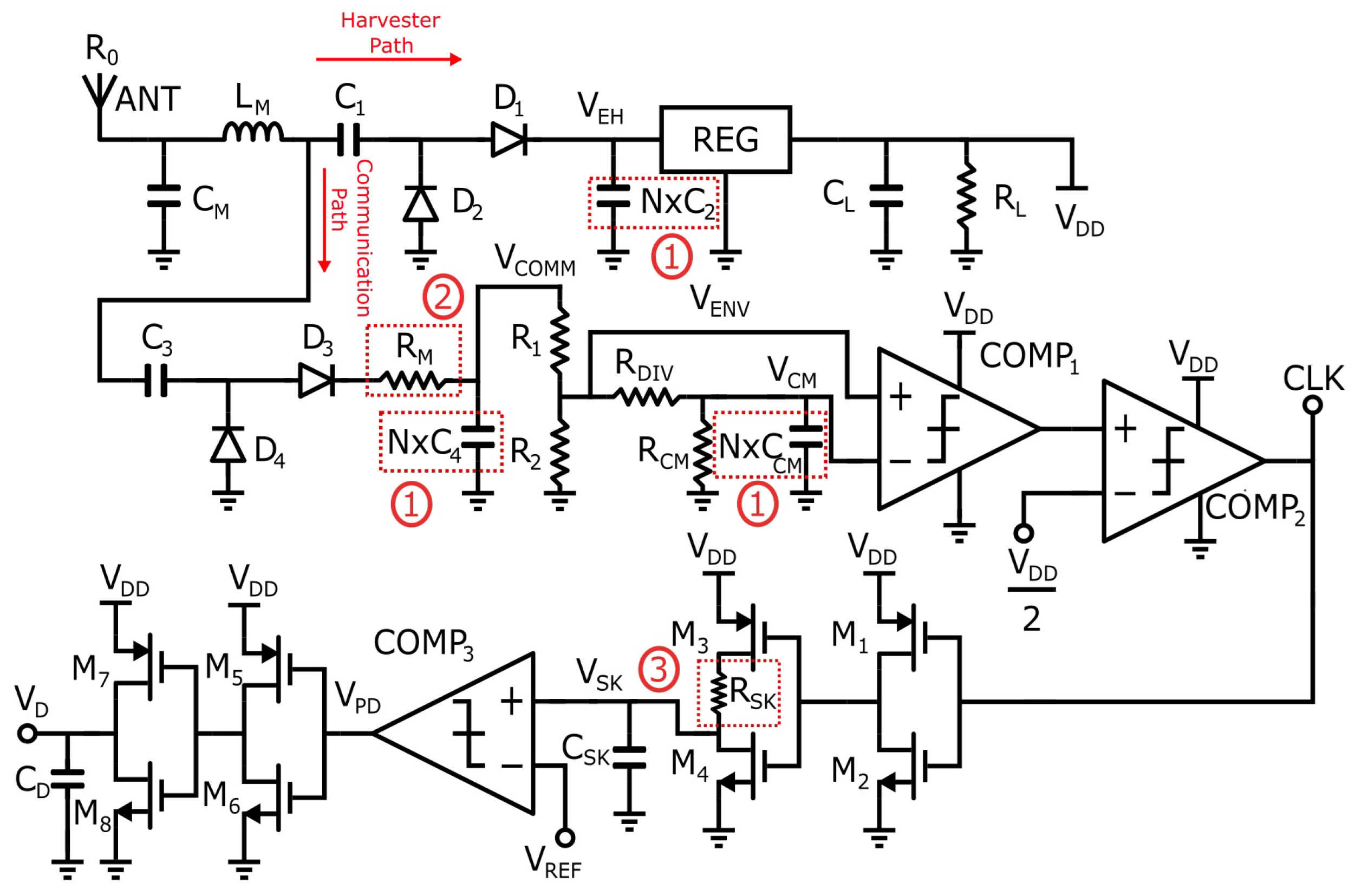
The complete circuit structure of the energy harvesting ASK-PWM system implemented using discrete components on PCB is shown in 
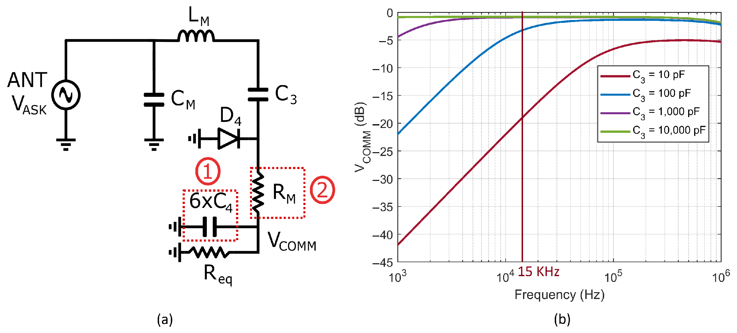
Figure 1. Also, the figure annotates with dashed lines the proposed solutions and improvements highlighted in the list of the previous section with their corresponding numbers. The structure comprises four main blocks: the receive antenna (ANT), the matching network, the harvesting path, and the communication path.
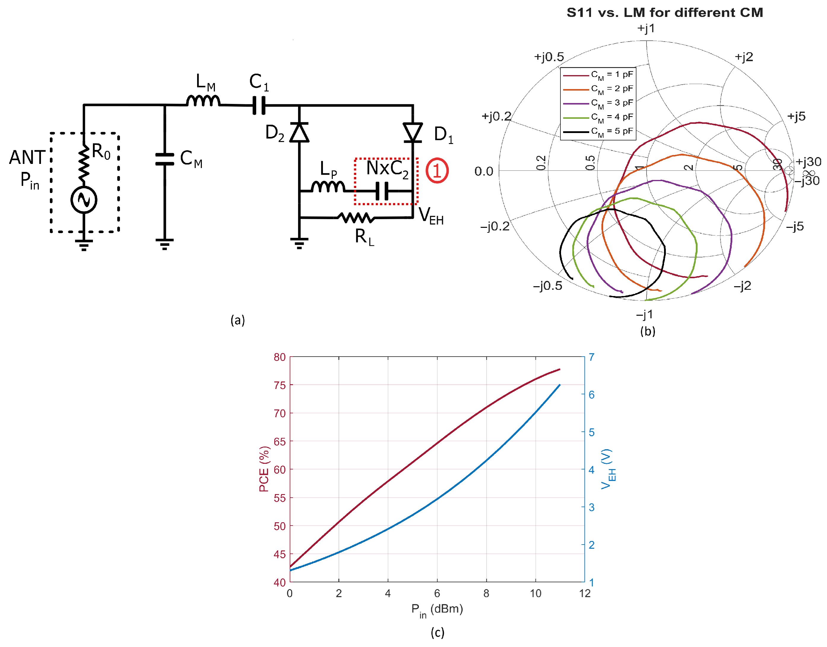
The receive antenna here collects the RF power and the ASK-PWM modulation signal. This antenna has a characteristic resistance R 0 . The matching network here was chosen to be a shunt capacitor C M series inductor L M , which does not perturb the low-frequency ASK-PWM signal. This network provides good matching between R 0 and the input impedance of the harvester path. L M here also provides resonance peaking for the RF voltage suitable for controlling the location of the peak efficiency of the harvesting rectifier.
Secondly, the harvester path contains a voltage doubler structure C 1 , D 1 , D 2 , C 2 , a voltage regulator R E G , load capacitance C L , load resistance R L , and regulated supply output V D D . Here, the voltage doubler should convert the RF input power into a DC voltage V E H that is higher than the necessary regulated output voltage V D D ; additionally, V E H should be given enough room for the modulation of ASK in such a way that the minimum peak voltage is higher than the regulated output voltage. C 1 , here, should be large enough to allow the input reactance to be dominated by D 1 and D 2 ; hence, this capacitor does not block RF power.
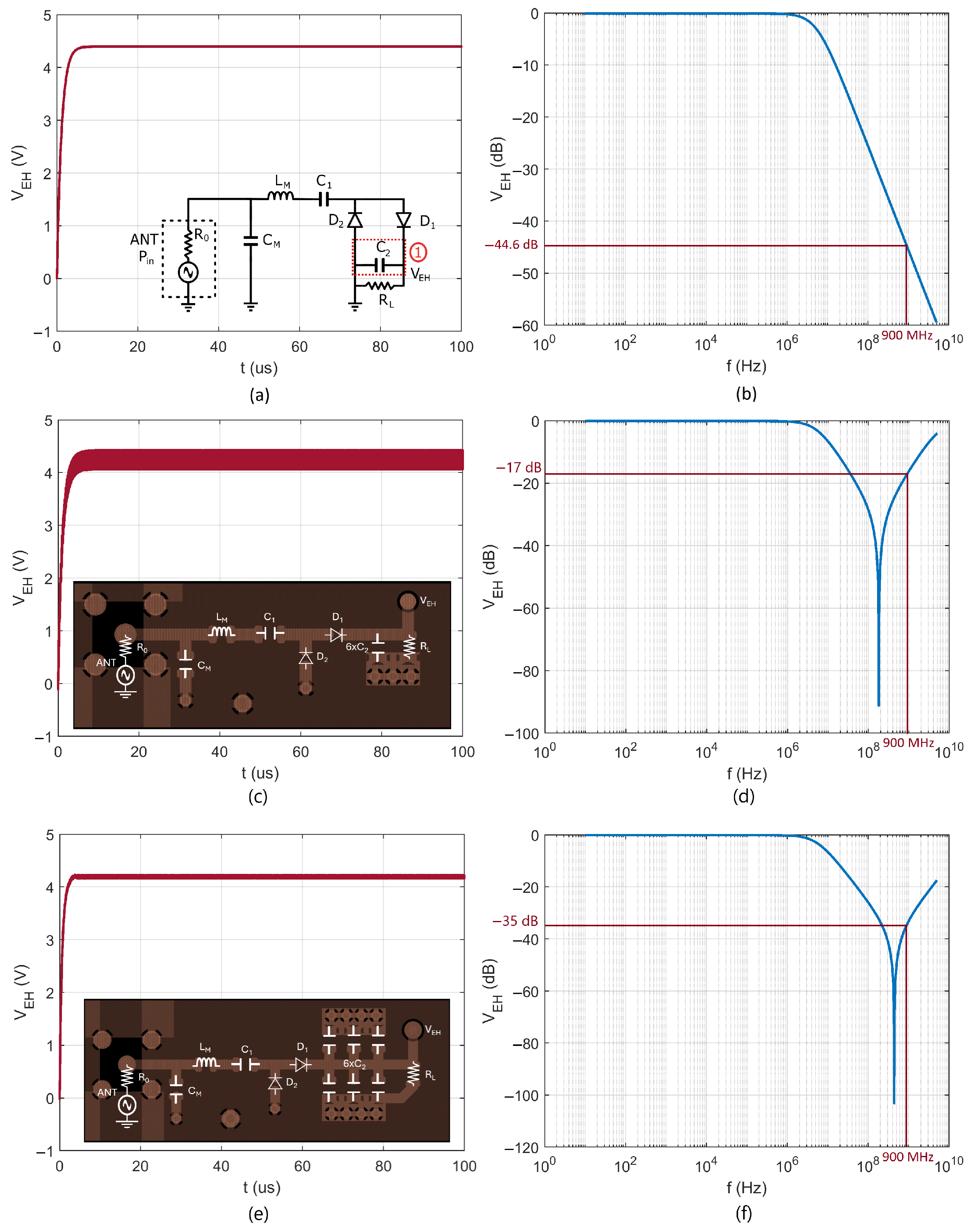
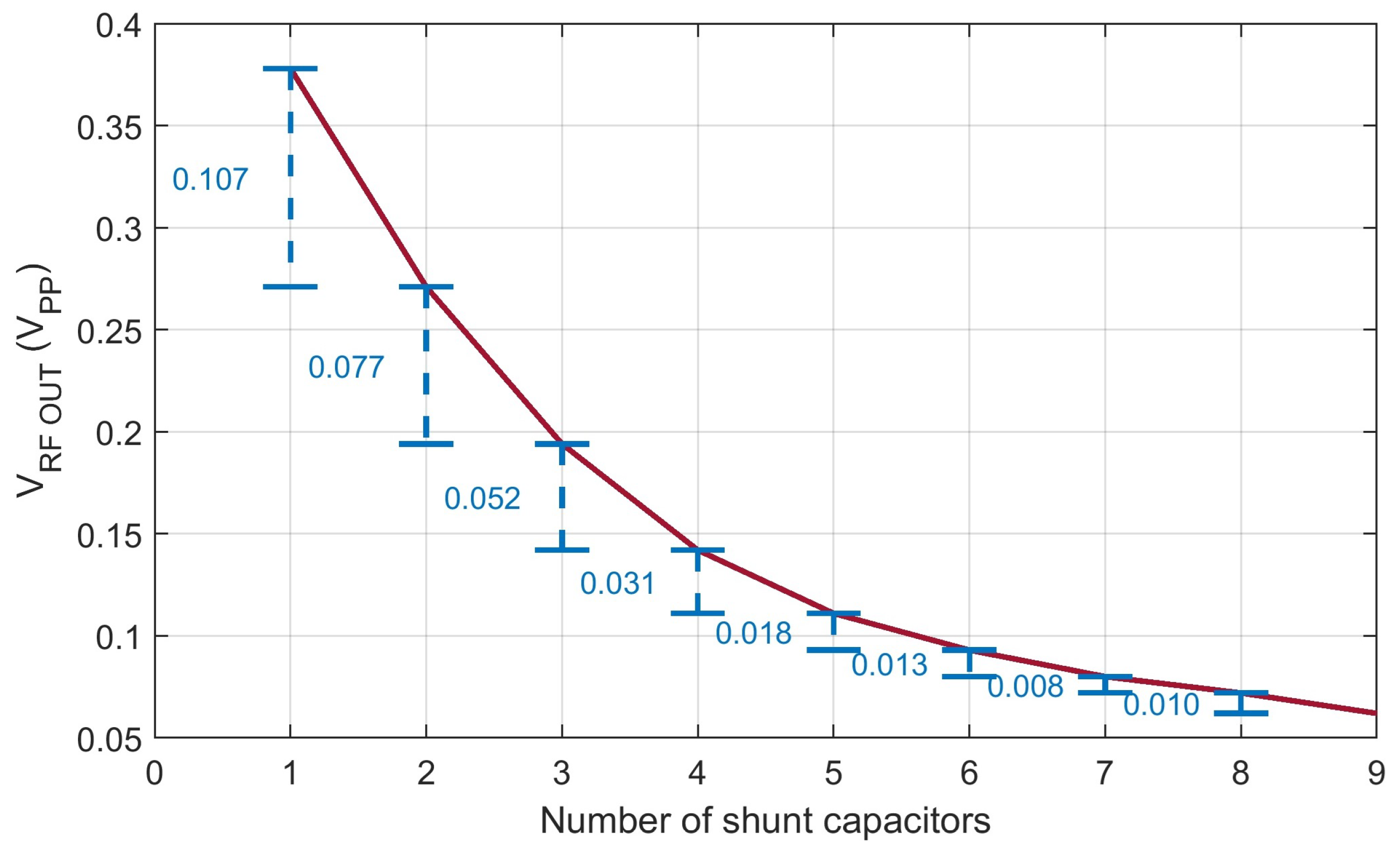
 N× C 2 combines N capacitors in a shunt to make a large capacitor (item ①). The main reason for this shunt combination is to reduce the inductive parasitic effects to improve the DC output smoothness; Section 3 will provide more details. The regulator provides a stabilized DC voltage that is not impacted by the ASK-PWM and switching noises from the system. It also powers up R L and supplies a stable voltage V D D to power up the system’s comparators and inverters. C L should be very large to filter any noises at the regulator’s output and help with the regulator’s frequency stability.
The communication path is composed of an ASK-PWM demodulator and decoder. It contains a voltage doubler C 3 , D 3 , D 4 , R M , C 4 , a voltage divider R 1 , R 2 , an ASK filter comprising R D I V , R C M , C C M , comparators C O M P 1 , C O M P 2 , a PWM decoder containing an inverter made out of M 1 , M 2 , a skewing inverter made out of M 3 , M 4 , R S K , C S K , comparator C O M P 3 , a delay buffer comprising M 5 , M 6 , M 7 , M 8 , and C D . In this communication path, C 3 is chosen to be in the nanofarad range to provide Alternating Current (AC) coupling. R M with the help of R 1 and R 2 is used to drop down the voltage of the voltage doubler to a value suitable for C O M P 1 (within the range of its input common-mode range I C M R ). Additionally, R M (item ②) provides isolation between the loading of the communication rectifier and the harvester rectifier by reducing the amount of current passing through it. This ensures the P C E is unimpacted by the changes in the loading of the communication rectifier and, hence, adds additional flexibility in tuning the time constants. This voltage doubler produces the communication voltage V C O M M , an ASK-PWM modulated signal.
As for the ASK filter, N× C 4 is made out of several parallel capacitors to reduce inductive effects, and it results in a time constant τ 1 , which can be approximated assuming R C M is in the megaohm range and the remaining resistors in the filter in the kiloohm range as:
τ 1 N C 4 ( R 1 + R 2 )
where R 1 and R 2 are used mainly to set up τ 1 with C 4 and divide the voltage even further for the filter. This combination produces the envelope voltage V E N V . The voltage division R D I V and R C M with C C M are used to establish the second time constant τ 2 , which can be approximated to:
τ 2 N C C M ( R D I V + R 2 )
This combination produces the common-mode voltage V C M . τ 1 here should be designed to be smaller than τ 2 to give V E N V enough voltage swing at the ASK-PWM frequency to be amplified by C O M P 1 ; τ 2 is designed to be about 100 times larger than τ 1 to reduce the ASK-PWM modulation. This is achieved by having C 4 in the lower sub 10 picofarad range while C C M is two orders of magnitudes larger (since R 1 , R 2 , and R D I V are in the 100 s kiloohms range). R C M should be in the megaohm range, and hence, the division between R D I V and R C M should be small. This is used to achieve two goals. The first is that by having such a small voltage division, V C M would be centered between the two peaks of V E N V , causing V C M to act as the average of V E N V and, hence, biases C O M P 1 as a common-mode DC voltage. The second goal is to never allow V C M to cross either peaks of V E N V during steady-state operation (i.e., during constant harvesting with no data transmission). As a result, C O M P 1 would amplify the difference between the two peaks of V E N V with the bias of V C M , and then it would go into C O M P 2 to maximize the voltage swing into square waves with a reference voltage V D D / 2 . The output of C O M P 2 produces the recovered clock C L K signal demodulated from the ASK modulation.
Moving on to the PWM decoder, after the inversion (through M 1 and M 2 ) of the C L K signal containing the PWM modulation, it passes through the skewed inverter ( M 3 , M 4 , R S K (item ③), C C K ) followed by C O M P 3 to extract the pre-data V P D . The skewing inverter with C O M P 3 is used to distinguish between bits “0” and “1” based on the pulse width of the C L K signal. If the pulse has a narrow-width high signal, it will be decoded as a “0”; if it has a wide-width high signal, it will be decoded as “1”. This is achieved by making the charging time for the skewing inverter long and by making the discharging time as fast as possible, after which C O M P 3 outputs a high signal only when its skewed input crosses its reference voltage V R E F , outputting bit “1”. Finally, V P D output from C O M P 3 goes through a buffer ( M 5 M 8 ) that adds a small delay using C D producing the final data output V D . This delay is necessary to synchronize the negative edge-trigger of C L K with V D so that the data can be stored and digitally processed for the designed application.
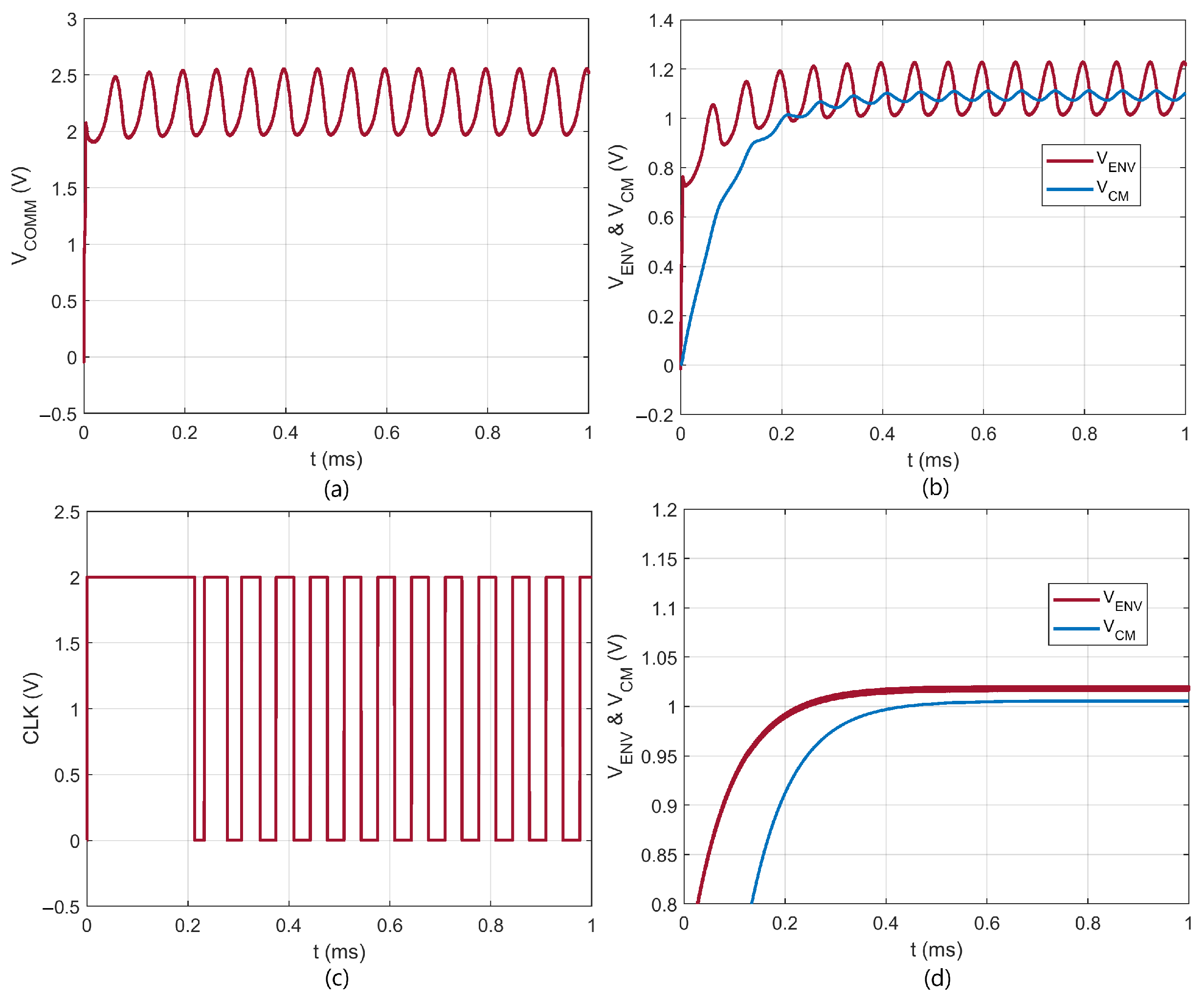
Figure 2 shows illustrative plots of the working principles of the ASK-PWM demodulator by modulating the RF power with the bit pattern “0010”. The plots show the voltage received by the antenna V A N T , and they also show V E N V , V C M , C L K , V S K , V R E F , V P D , and V D . The plots also highlight the synchronization between C L K and V D with red dashed lines, as discussed.

3. Design Phases and Proposed Solutions

This section presents the design phases leading to the complete PCB implementation. In these phases, we will show the design approaches, ideas, and proposed solutions that would allow the complete PCB to be implemented in a discrete format.

3.1. Phase 1: Voltage Doubler Design with Parasitic Inductance Impact and Reduction

In the design of a voltage doubler, system analysis led to the definition of the targeted specifications. The harvesting frequency is 900 MHz; the harvested voltage should be at 4 V, while the power delivered should be at 4 mW with a P C E > 50%. Figure 3a shows the schematic of the voltage doubler implemented in the Advanced Design System (ADS). L P was added to model the parasitic inductance due to the trace and ground vias, which was set to zero initially. The capacitance C 1 is a 10 pF capacitor for the reasons highlighted in the previous section, and N× C 2 is a 6 × 100 pF capacitor made large to reduce the capacitive ripples at the harvested output voltage node. R L is made of 4 k Ω such that when harvesting 4 V, the power is at 4 mW. The diodes are SMS3922-079LF from Skyworks Solutions Inc., which are sourced from Irvin, CA, USA, and their SPICE model can be found in the datasheet. The matching network is designed by sweeping L M from 1 nH to 100 nH while parametrically sweeping C M . Figure 3b shows the S 11 plotted on a Smith chart using Large-Signal S-Parameter (LSSP) simulation. Each circle on the Smith chart represents a C M plotted for the various L M values. Values of L M = 33.68 nH and C M = 2 pF were selected to match the input of the RF voltage doubler to 50 Ω (these values, however, will be modified with PCB layout design). Figure 3c shows the simulated DC harvested voltage and P C E , obtaining 4.2 V with a P C E of 71.0 % at a P i n = 8 dBm.
A transient simulation was performed to the circuit in Figure 3a with L P removed, as shown in Figure 4a. It can be noticed that the transient simulation is free from both ripples and RF variations due to the good rejection of the output filter to the RF and any of its harmonics. The output filter’s response is shown in Figure 4b, which resembles a low-pass filtering operation, rejecting the 900 MHz RF and its harmonics. An initial layout using an FR4 substrate with a 0.6 mm thickness was created to produce a reliable simulation, as shown in Figure 4c. A transient co-simulation was performed to visualize the output DC voltage of the harvester, as shown in the figure. As can be seen from the figure, the amount of RF content was large and was not related to how large C 2 was. By looking at the frequency response of the output filter, shown in Figure 4d, we can see that the response now is a notch filter, which is caused by the inductive path of the rectification filter through the vias to the ground plane. This was modeled in the ideal schematic of Figure 3a by making L P = 1.2 nH, which reproduced the results in Figure 4c,d. The output filter response can be written as follows:
V out ( s ) V in ( s ) = R L R 0 + R L s 2 + N L P C 2 s 2 + s R 0 R L R 0 + R L N L P + N L P C 2
which confirms the output filter response as a notch filter, which has a resonance frequency f 0 at:
f 0 = 1 2 π N L P C 2
From Equation (4), it can be deduced that by increasing N (increasing the number of parallel capacitive branches while keeping the cumulative capacitance the same), it would effectively reduce the inductive parasitic effect and, hence, f 0 would increase. As f 0 increases, the 3-dB half power frequencies also increase, which improves the rejection at 900 MHz. After this analysis, we split the 600 pF capacitor into 6 × 100 pF capacitors in parallel, as shown in Figure 4e. The transient co-simulation presented in Figure 4e shows that the intensity of RF leakage has reduced drastically after the splitting of capacitances, which reduced the amount of inductance through the vias to the ground plane. Shunting multiple paths with multiple capacitances will reduce the equivalent inductance since L P will be divided approximately by the number of shunt capacitances. The frequency response is shown in Figure 4f where the increase in f 0 is noticeable; hence, the rejection of the RF at 900 MHz is improved from −17 dB to −35 dB. Although an increase of f o can be achieved by reducing C 2 instead of L P , which would also reduce the RF leakage into the output, it would increase the amount of capacitive ripples, which are unwanted. Hence, reducing L P while keeping C 2 large would reduce both capacitive ripples and RF leakage. This technique was applied throughout the work to reduce the amount of voltage ripples and RF leakage at critical nodes.
We conclude our analysis of this phase with the relation between the number of parallel capacitive branches and the amount of RF leakage into the output of the harvesting rectifier. Figure 5 shows the amount of RF leakage vs. the number of parallel branches with annotated differences between consecutive data points. It can be noticed from the plot that, as we increase the number of branches, the RF leakage reduces as expected. It is noted that the incremental benefits reduce with each additional branch, indicating a point of diminishing returns where a further increase in the number of capacitive branches yields progressively smaller improvements. We have chosen six as an appropriate number of elements since they can be compactly placed on the PCB while efficiently reducing RF leakage into the output.

3.2. Phase 2: Interfacing Harvester Path with Communication Path

The second phase is related to the interface between the harvester path and the communication path, which is shown in Figure 6. In this schematic, we modeled the output of the communication’s rectification load with a shunt capacitance C 2 and R e q , where R e q is approximately the series combination of R 1 and R 2 in Figure 1. The values of the matching network here do not change from that of phase 1 due to the inclusion of R M , which isolates the power from the two main paths. A critical time constant that allows the ASK modulation to reach the output node of the communication path is τ 3 , which can be written approximately as:
τ 3 C 3 ( R e q + R M )
where R e q is set at 150 k Ω initially to reduce the current amount through the communication path. This time constant results in a high-pass operation; hence, C 3 should be designed to be large enough to allow the ASK to pass to the output of the communication path. Figure 7a shows the testbench for the AC simulation to obtain the frequency response at the output, which is plotted in Figure 7b for different values of C 3 . Since we are designing the bit rate at a low value (15 kbps) to reduce dynamic power consumption, we chose C 3 to be at 1000 pF, which would result in a τ 3 = 150 μs, which translates to a cutoff frequency for the high pass response at 964 Hz. A plot of the transient response of the circuit in Figure 6 is shown in Figure 8a,b using C 3 = 10 pF and 1000 pF, respectively. We can see that we can obtain the modulation correctly according to the calculations and frequency response.
Since a voltage doubler is used in the communication’s path and R e q is large, the output voltage may be too high for the I C M R range of C O M P 1 . For that reason, a lossy resistor R M was added in the series path of D 3 in the communication’s path to reduce the output voltage. Additionally, a split of R e q into R 1 and R 2 was performed to drop the voltage further. R M also serves another purpose: it reduces the impact of changing R e q in the communication’s path on the P C E of the harvester path. Figure 9a,b show that without having R M , changing R e q leads to voltage reduction at the output of the communication’s path but at the cost of a drastic decrease in P C E in the harvesting path. However, when placing R M , the amount of current flowing through D 3 and D 4 is reduced drastically, which allows the voltage to be dropped while keeping the P C E high in the harvesting path, regardless of variations in R e q as shown in Figure 9c,d. This adds additional flexibility since now R e q can be used to adjust τ 1 , τ 2 , and τ 3 with minimal impact on the P C E of the harvester. In a sense, the inclusion of R M provided good isolation between the harvester and communication paths. Furthermore, the transition in V C O M M is more linear in Figure 9c compared to Figure 9a, allowing for a more flexible voltage level choice for V C O M M . Despite the attenuation that may occur in the communication path’s rectifier due to the addition of R M , the cascaded comparators and the sustainable amount of power being harvested would still guarantee successful demodulation of the ASK signal.
As for R M ’s value selection, two objectives must be met. The first is achieving good isolation between the harvester and communication paths, such that when changing R e q , the P C E of the harvester path remains constant. The second is to reduce V C O M M to an appropriate voltage (center of I C M R of C O M P 1 ). Both objectives are achieved when increasing R M , which results in better isolation and reduces the impact of R e q on the P C E of the harvester path due to the current reduction in the communication paths discussed above. However, when R M increases, the attenuation and drop in V C O M M increases; additionally, decreasing R e q , further adds to the attenuation and voltage drop, as was shown in Figure 9c. An appropriate value of R M can be selected by first choosing both an R e q that tunes τ 1 with C 4 , and an R 2 that tunes τ 2 with C C M ( R 1 is simply obtained by calculating R e q R 2 ); then, R M is increased gradually in the simulations until the P C E of harvester’s path is maximized and V E N V is at around the middle of I C M R of C O M P 1 .
As for the P C E simulations and measurements, a co-simulation was performed of the circuit in Figure 6. For harvesting a DC power of 4 mW, a P C E of 56.55% was obtained as opposed to the ideal schematic’s P C E of 62.5%. For a 2 mW harvested power, the P C E was co-simulated at 51%. The latter P C E was used as a comparative reference when the 2 V regulator was applied to a 2 k Ω load, which provided a power delivery of 2 mW. A prototype was built for this phase, measuring a P C E of 42.12% for an output power of 2 mW.

3.3. Phase 3: ASK Filter and Demodulator

As for the design of the ASK filter and demodulator, the design is mainly concerned with the following: the appropriate envelope voltage swing needs to be close to the center of the I C M R of the comparator, the extracted common mode voltage should be close to the center of the envelope and as constant as possible, and the comparators should produce square waves for clock recovery. For this part, we set R M = 15 k Ω (tuned to 100 k Ω after layout), with R 1 and R 2 both being 75 k Ω and C 4 = 1 pF. This led to V C O M M centered at 2.3 V with AM modulation at 15 KHz, as shown in Figure 10a. This voltage was dropped by half to be close to the center of a full-swing I C M R of a 2V-operated C O M P 1 , which is shown as V E N V in Figure 10b. τ 1 from Equation (1) was calculated as 900 ns, which translates to a low-pass cutoff frequency of 176.8 KHz, which passes the 15 kHz modulation frequency while attenuating the 900 MHz RF frequency. As for τ 2 from Equation (2), with R D I V = 150 k Ω , R C M = 8 M Ω , and C C M = 100 pF, it would be equal to 135 μs, which gives a low-pass cutoff frequency of 1.18 kHz, which removes the ASK modulation from V C M but keeps the DC average of V E N V , as shown in the blue wave in Figure 10b. The wide range of values selected between τ 1 , τ 2 , and τ 3 allows for successful demodulation of the ASK for different modulation frequencies ranging from 4 KHz up to 150 KHz. As a result of this wide range, any small variance that may be caused by the selected component would still allow for correct clock recovery. The ASK filter is also dynamic in the sense that if the power changes in a way that still keeps the envelope voltage inside the I C M R of C O M P 1 , the common mode voltage would track the average of the envelope, maintaining the correct operation of C L K generation. Additionally, due to V C M being extracted from V E N V , they would be in sync; hence, the C L K signal is synced to the frequency of V E N V and V C M , regardless of the phase difference between the two latter signals. The C L K signal coming from C O M P 2 is shown in Figure 10c. Note that V C M is not centered exactly in the middle of V E N V due to the voltage division between R D I V and R C M , which brings V C M down by 2%, which reduces switching errors during idle state (no data transmission), as shown in Figure 10d. It takes two “0” bits to bring the system from an idle state to the data transmission state. As for the response time of the demodulator, it is limited by the start-up conditions of the demodulator, which is about 0.2–0.3 ms for this specific design choice, which is comparable to that of the regulator’s output time constant.

3.4. Phase 4: PWM Decoder

As discussed in Section 2, the PWM decoder requires a skewing operation for data decoding. The skewing operation is traditionally implemented by making the transistor length M 3 large enough to result in the skewing operation by increasing the RC charging time constant while making the aspect ratio ( W / L ) 4 as high as possible to allow for a fast discharge time. The former is easy to implement on an IC since there is flexibility in increasing the length of the transistor; however, in discrete PCB implementation, this flexibility is not an option. For this reason, we implemented a solution shown in the inverter M 3 and M 4 of Figure 1. By adding the skewing resistor R S K between the drain of M 3 and the output of the inverter, we can increase the charging time constant by increasing the resistance of the charging path without impacting the discharge path. C S K was also added to the output of the skewing inverter to support this time-constant increase. We denote this time constant as τ 4 , which can be written as:
τ 4 C S K ( R S K )
C S K = 100 pF was chosen while R S K = 250 k Ω . This leads to a time constant of 25 μs. For a 33 μs bit “0” pulse at a supply of 2V, it translates to 1.466 V of peak charging voltage, while a wide pulse of 99 μs indicating bit “1” has a peak charged voltage of 1.96 V. These values are smaller by about 0.4 V in simulations due to the zero undershoot of the gate-to-drain capacitors. Hence, we chose a reference of 1.5 V to distinguish between bits “0” and “1”. Figure 11a shows a simulation plot of the C L K signal sending a repetitive pattern of “0010” to the skewing inverter. Figure 11b shows the skewing operation of the proposed PWM decoder, while Figure 11c presents the data recovery simulation based on the C L K signal’s width.

4. Complete PCB Measurement and Validation

To validate the implementation of such a system in discrete format with the proposed solutions and improvements, we implemented the system entirely on a two-layer FR4 substrate of size 5 cm × 4 cm × 0.6 cm. An FR4 substrate was chosen to minimize the cost and production time without compromising significant performance, which lines up with the objectives of this work. The first layer contains all the components and interconnects, while the second layer is the ground plane. The PCB is shown in Figure 12a with the annotated circuit blocks. L M is an RF inductor from Murata LQW15AN5N2B80D sourced from Kyoto, Japan. The inductor has a value of 5.2 nH and a Q factor of 70 at 900 MHz. This inductor’s Self-Resonance Frequency S R F is 8 GHz, which is about 9 times higher than the harvesting frequency. The diode is SMS3922-079LF from Skyworks in Irvine, CA, USA: a Schottky diode with a low turn-on voltage, series resistance, and junction capacitance. The breakdown voltage is 8 V, which is suitable for the maximum voltage level in our design. The regulator used is a TLV70220PDBVR manufactured by Texas Instruments in Dallas, TX, USA. This part regulates the voltage at 2 V, draws a bias current of 35 μA only, which makes it suitable for harvesting applications, and has a Power Supply Rejection Ratio P S R R of 68 dB at 1 kHz. Stabilization for this regulator was achieved by making C L = 100 nF and 6 × C 2 = 600 pF. As for the comparator, BU5265HFV-TR was chosen from Rohm Semiconductor in Japan, which has full input swing and can operate at a V D D range from 1.8 to 5.5 V, suitable for our 2 V regulator. The supply current of this comparator is at a low value of 22 μA, making it ideal for harvesting. The maximum clock frequency for such a comparator is 14.28 MHz, which is more than enough for the bitrate of our system. It is critical to note that these comparators are CMOS and, hence, do not load the ASK filter, especially with the 8 M Ω resistor R C M shunted with the input of the comparator. The inverters are made out of bsh103bk NMOS and bsh205g2 PMOS, which are made by Nexperia in USA. The NMOS has a typical threshold voltage of 1 V, while the PMOS has a typical threshold voltage of −0.7 V. Both are suitable for a 2 V supply. The maximum switching frequencies for the NMOS and PMOS are 166.67 MHz and 33.33 MHz, respectively, higher than the designed data rate. The dynamic power consumption of these inverters is at 3 μW at a switching frequency of 15 KHz, 100 pF loading and 2 V supply power, which are reasonable for harvesting. The total power consumption of the system was 355 μW. R S K here is made out of a potentiometer to tune τ 4 to control the peak of the skewing output voltage of different bits. As a result, by adjusting the potentiometer, successful bit decoding can be ensured when re-configuring the bit rate for the system.
The measurement setup of radiative field harvesting is shown in Figure 12b. A signal generator SME 06 from Rhode & Schwarz was used to produce an ASK-PWM modulated wave. The output power of the signal generator was set at 16 dBm (calibrated to output 12 dBm) at a frequency of 924 MHz. Although the SME 06 is capable of digital modulation, it does not perform ASK modulation directly. To solve this problem, we controlled the digitally controlled attenuator using a bit pattern at a switching rate of 30 KHz to achieve ASK-PWM modulation. We assigned a 99 μs wide-high pulse followed by a 33 μs of narrow-low pulse for bit “1”, and assigned a 33 μs narrow-high pulse followed by a 33 μs of narrow-low pulse for bit “0”. The signal generator was connected to an 8 dBi HG908PCR Right-Half Circular Polarized (RHCP) commercial antenna. Another antenna was connected to the PCB. Both antennas were characterized using a Vector Network Analyzer (VNA), presenting close to 50 ohms impedances near the 924 MHz frequency. Hence, we operated at that frequency. The separation distance between the antennas was kept at 8 cm. However, the system operated correctly from 6 cm up to 12 cm. The PCB contained several test points connected to the hlRTB2004 Rhode & Schwarz oscilloscope to obtain waveform measurements. The regulator powered up all the inverters and comparators in the PCB; hence, no power supply was needed. All the required references for the comparators were set by voltage division with respect to the regulator voltage. The regulator’s enable pin was connected to V E H , which needs to be maintained above 2 V to keep the regulator in normal operating condition.
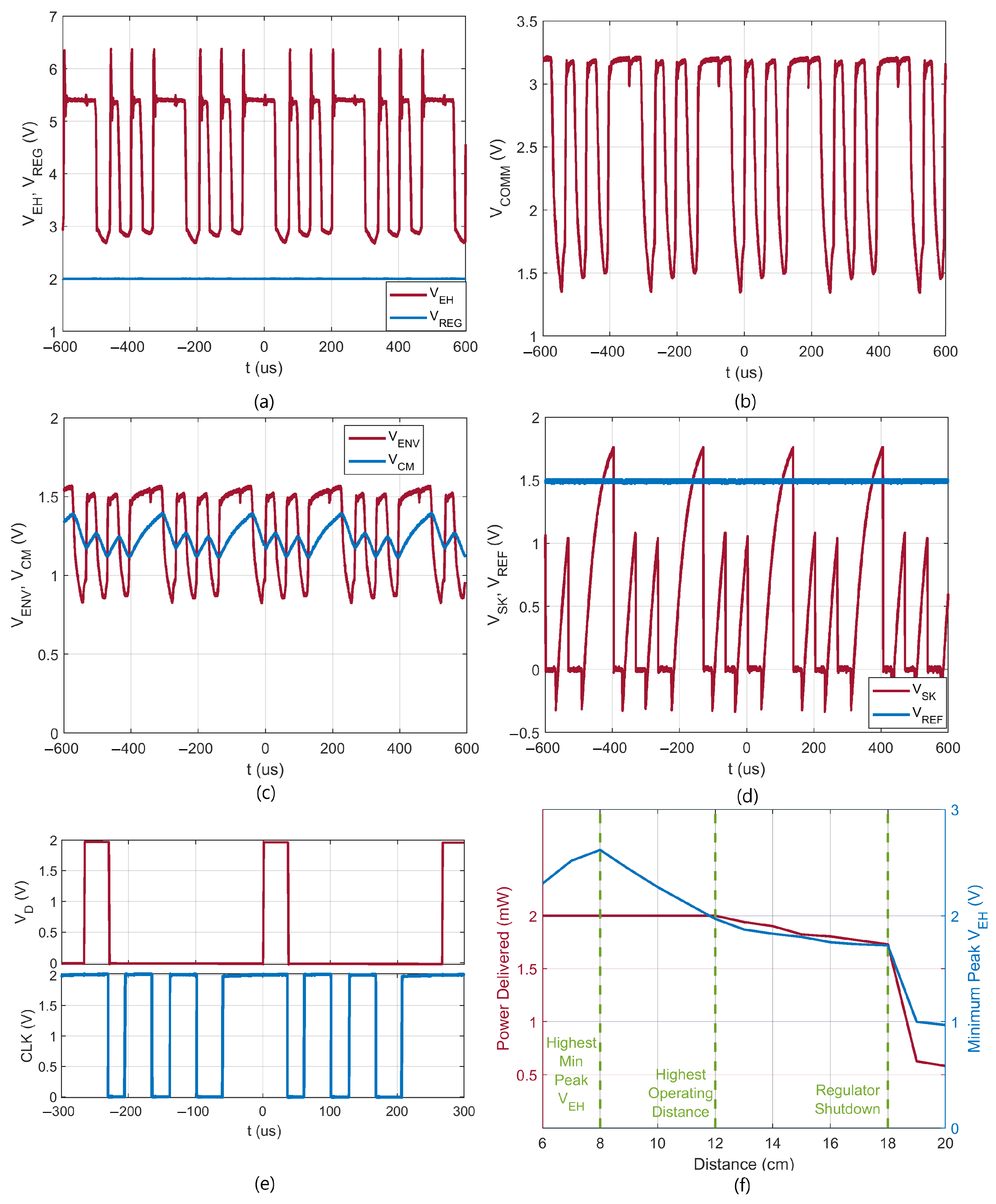
Figure 13 shows the most critical measurements of the PCB in Figure 12a. Figure 13a shows the harvested voltage V E H and regulated voltage V R E G . A bit pattern of “100” was transmitted repeatedly, as shown in the red wave in the figure. The voltage swung from 5.2 V to 2.9 V, centered at 4.2 V. The voltage was never below 2 V, keeping the regulator at the correct normal operating condition. The blue wave shows the regulator output voltage was constant at 2 V regardless of variations in the harvested voltage due to modulation. This 2 V was applied to an R L of 2 k Ω , hence delivering a power of 2 mW at a total receiver efficiency of 12.5%. Figure 13b shows V C O M M being dropped by R M down to 2.31 V, swinging up to a maximum of 3 V and a minimum of 1.32 V. R 1 and R 2 dropped this voltage by half, as seen by the blue wave in Figure 13c, producing V E N V . We can note that the V E N V range was between 1.5 V and 0.73 V, within the I C M R of C O M P 1 . V C M is also shown as the blue line in Figure 13c. Figure 13d presents the output of the proposed skewing inverter (red) and the reference voltage (blue) used to distinguish between a wide- and a narrow-high pulse. Figure 13e shows the data output V D (red) correctly presenting bit “1” for a wide pulse and bit “0” for a narrow pulse. Also, shown in the same plot, the C L K was produced from V E N V , V C M , C O M P 1 , and C O M P 2 . The system performed correct data and clock recovery even with different data bits transmitted due to the asynchronous extraction of both voltages. As for the separation distance validation, a plot showing the relationship between both the minimum peak V E H and power delivered by the regulator vs. the separation distance between the antennas is shown in Figure 13f. We can note three critical regions on the plot: The first is at 8 cm where efficient polarization was achieved and, hence, the highest minimum peak V E H was achieved. The second is after 12 cm where minimum peak V E H 
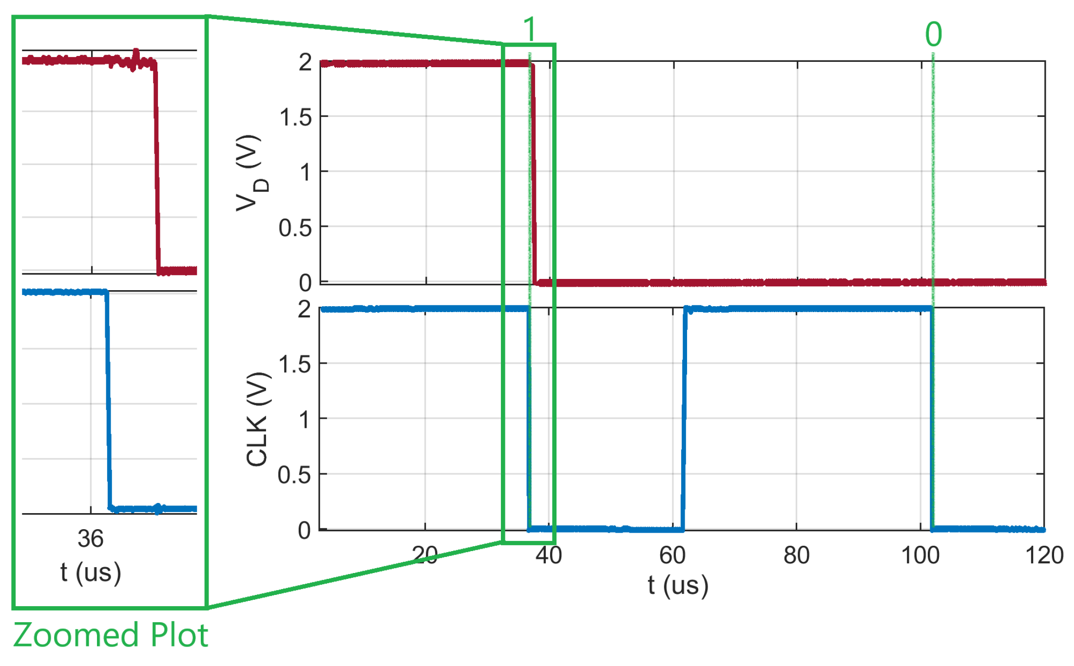
dropped below 2 V, which caused the regulator voltage to drop below 2 V. The last region is after the 18 cm mark, where the internal reference inside the regulator collapsed completely and the power plummeted. As a result, the system operated correctly and provided a constant 2 mW power at a separation distance between 6 cm and 12 cm. Finally, The synchronization between V D and C L K is shown in Figure 14. For bit “1”, the C L K signal dropped before V D ; hence, a bit “1” would be stored in a shift register with a negative edge trigger. When the C L K triggered negatively and there was no high signal, it would record a bit “0”.
A comparison between this work and the previous literature is shown in Table 1. We can note that this work is the only work that implemented an ASK-PWM harvesting system on an FR4 substrate using discrete components only. Additionally, the separation distance is the largest at a 12 cm distance.

5. Conclusions

This paper presented a radiative-field ASK-PWM decoded energy harvester implemented using discrete components. The paper presented the design approach, proposed solutions, and improvements to the PCB design. One solution targeted the inductive voltage parasitic effect existing at the harvested voltage, which was solved using parallel connections of rectification capacitors to reduce inductive effects. A lossy resistor to the communication rectifier was added to isolate the current between the harvester path and the communication path to minimize the impact on P C E ; this also allows for additional flexibility in tuning the time constants without impacting the P C E . A skewing inverter was implemented using a skewing resistor to achieve the skewing operation instead of the typical design, which is challenging to accomplish on a PCB design. The design was implemented and validated on an FR4 substrate using radiative field measurements at 924 MHz at a bit rate of 15 kbps, consuming a power of 355 μW. It also presented correct harvesting operation and data and C L K recovery from 6 to 12 cm of antenna separation. The work presented is targeted to allow the option of designing an ASK-PWM decoded harvester on an FR4 substrate instead of IC realization and to enable the implementation to target several applications other than biomedical applications at a low cost and reduced manufacturing time.

Author Contributions

Conceptualization, M.A.S.; methodology, M.A.S.; software, M.A.S. and R.E.A.; validation, M.A.S.; formal analysis, M.A.S.; writing—original draft preparation, M.A.S.; writing—review and editing, M.A.S., R.E.A., M.C.-E.Y. and A.M.A.; visualization, M.A.S., R.E.A., M.C.-E.Y. and A.M.A.; supervision, R.E.A. and M.C.-E.Y.; funding acquisition, R.E.A. and M.C.-E.Y. All authors have read and agreed to the published version of the manuscript.

Funding

This research received no external funding.

Data Availability Statement

Data are included in the article.

Conflicts of Interest

The authors declare no conflicts of interest.

References

  1. Lim, J.; Lee, B. Carrier Harmonic Modulation for Simultaneous Wireless Information and Power Transfer. IEEE Access 2023, 11, 135568–135574. [Google Scholar] [CrossRef]
  2. Dhull, P.; Schreurs, D.; Paolini, G.; Costanzo, A.; Abolhasan, M.; Shariati, N. Multitone PSK Modulation Design for Simultaneous Wireless Information and Power Transfer. IEEE Trans. Microw. Theory Tech. 2024, 72, 446–460. [Google Scholar] [CrossRef]
  3. Yang, Z.; Gan, C.; Shi, H.; Chen, Y.; Ni, K.; Qu, R. Simultaneous Wireless Power and Data Transfer System With Single Coil Based on Multifrequency Modulation. IEEE Trans. Ind. Electron. 2024, 71, 5714–5724. [Google Scholar] [CrossRef]
  4. Arakawa, T.; Krogmeier, J.V.; Love, D.J. Theoretical and Practical Analysis of MIMO Simultaneous Wireless Information and Power Transfer Over Inductively Coupled Circuits. IEEE Trans. Antennas Propag. 2024, 72, 2780–2789. [Google Scholar] [CrossRef]
  5. Barbruni, G.L.; Rodino, F.; Ros, P.M.; Demarchi, D.; Ghezzi, D.; Carrara, S. A Wearable Real-Time System for Simultaneous Wireless Power and Data Transmission to Cortical Visual Prosthesis. IEEE Trans. Biomed. Circuits Syst. 2024, 18, 580–591. [Google Scholar] [CrossRef] [PubMed]
  6. Jing, Y.; Feng, W.; Qiao, K.; Yang, L.; Wang, S.; Lu, L. Simultaneous Wireless Power and Data Transfer System With Full-Duplex Mode Based on LCC/CLC Resonant Network. IEEE Trans. Power Electron. 2023, 38, 5549–5560. [Google Scholar] [CrossRef]
  7. Hannan, M.A.; Abbas, S.M.; Samad, S.A.; Hussain, A. Modulation techniques for biomedical implanted devices and their challenges. Sensors 2012, 12, 297–319. [Google Scholar] [CrossRef] [PubMed]
  8. Anthes, J.P. OOK, ASK and FSK Modulation in the Presence of an Interfering Signal. 1998. Available online: https://www.tekassociates.biz/ook.pdf (accessed on 29 December 2024).
  9. Presi, M.; Artiglia, M.; Ciaramella, E. Electrical filter-based and low-complexity DPSK coherent optical receiver. Opt. Lett. 2014, 39, 6301–6303. [Google Scholar] [CrossRef] [PubMed]
  10. AL-Kalbani, A.I.; Yuce, M.R.; Redouté, J.M. Performance of a biomedical implant communication system using PWM coded ASK. In Proceedings of the 2012 International Symposium on Communications and Information Technologies (ISCIT), Gold Coast, Australia, 2–5 October 2012; pp. 133–138. [Google Scholar] [CrossRef]
  11. Yakovlev, A.; Jang, J.H.; Pivonka, D. An 11 μW Sub-pJ/bit Reconfigurable Transceiver for mm-Sized Wireless Implants. IEEE Trans. Biomed. Circuits Syst. 2016, 10, 175–185. [Google Scholar] [CrossRef] [PubMed]
  12. Fiore, V.; Ragonese, E.; Abdinia, S.; Jacob, S.; Chartier, I.; Coppard, R.; van Roermund, A.; Cantatore, E.; Palmisano, G. 30.4 A 13.56 MHz RFID tag with active envelope detection in an organic complementary TFT technology. In Proceedings of the 2014 IEEE International Solid-State Circuits Conference Digest of Technical Papers (ISSCC), San Francisco, CA, USA, 9–13 February 2014; pp. 492–493. [Google Scholar] [CrossRef]
  13. Rezaeiyan, Y.; Koolivand, Y.; Zamani, M.; Shoaei, O.; Akbari, M.; Moradi, F.; Tang, K.T. A 4.5 μW Miniaturized 3-Channel Wireless Intra-Cardiac Acquisition System. IEEE Trans. Biomed. Circuits Syst. 2023, 17, 1097–1110. [Google Scholar] [CrossRef] [PubMed]
  14. Pivonka, D.; Yakovlev, A.; Poon, A.S.Y.; Meng, T. A mm-Sized Wirelessly Powered and Remotely Controlled Locomotive Implant. IEEE Trans. Biomed. Circuits Syst. 2012, 6, 523–532. [Google Scholar] [CrossRef]
  15. Zhong, X.; Sham, C.W. An SoC for Qi-compliant Wireless Power Transmitter with Enhanced EMI Performance. In Proceedings of the 2019 6th International Conference on Systems and Informatics (ICSAI), Shanghai, China, 2–4 November 2019; pp. 725–728. [Google Scholar] [CrossRef]
  16. Barakat, A.; Bin Zulkalnain, M.K.; Pokharel, R. Comparator-less ASK-PWM CDR Circuit for Forward Data Communication Over A Single Channel Wireless Power and Data Transfer System. In Proceedings of the 2023 IEEE Wireless Power Technology Conference and Expo (WPTCE), San Diego, CA, USA, 4–8 June 2023; pp. 1–4. [Google Scholar] [CrossRef]
  17. An, S.K.; Park, S.I.; Jun, S.B.; Lee, C.J.; Byun, K.M.; Sung, J.H.; Wilson, B.S.; Rebscher, S.J.; Oh, S.H.; Kim, S.J. Design for a Simplified Cochlear Implant System. IEEE Trans. Biomed. Eng. 2007, 54, 973–982. [Google Scholar] [CrossRef] [PubMed]
  18. Leung, V.W.; Cui, L.; Alluri, S.; Lee, J.; Huang, J.; Mok, E.; Shellhammer, S.; Rao, R.; Asbeck, P.; Mercier, P.P.; et al. Distributed Microscale Brain Implants with Wireless Power Transfer and Mbps Bi-directional Networked Communications. In Proceedings of the 2019 IEEE Custom Integrated Circuits Conference (CICC), Austin, TX, USA, 14–17 April 2019; pp. 1–4. [Google Scholar] [CrossRef]
  19. Habibagahi, I.; Jang, J.; Babakhani, A. Miniaturized Wirelessly Powered and Controlled Implants for Vagus Nerve Stimulation. In Proceedings of the 2022 IEEE Radio Frequency Integrated Circuits Symposium (RFIC), Denver, CO, USA, 19–21 June 2022; pp. 51–54. [Google Scholar] [CrossRef]
Figure 1. Proposed harvesting ASK-PWM circuit with contribution highlighted in dashed boxes.
Electronics 14 00485 g001
Figure 2. Illustrative plots of ASK-PWM demodulator and decoder.
Electronics 14 00485 g002
Figure 3. Voltage doubler design in ADS: (a) schematic, (b) matching simulation, and (c) V E H (blue) and P C E (red) simulations.
Electronics 14 00485 g003
Figure 4. Inductive parasitic effect on harvested voltage: (a) transient simulations of schematic without L P , (b) schematic’s frequency response, (c) original layout with transient co-simulation, (d) original layout’s frequency response, (e) modified layout with transient co-simulation, and (f) modified layout’s frequency response.
Electronics 14 00485 g004
Figure 5. A plot showing the relationship between the RF swing at the output and the number of shunt capacitive branches with blue dashed lines highlighting successive voltage reduction.
Electronics 14 00485 g005
Figure 6. Interface between harvester and communication paths.
Electronics 14 00485 g006
Figure 7. Frequency response of the communication path: (a) test bench schematic, and (b) simulation with different C 3 values.
Electronics 14 00485 g007
Figure 8. Transient response of the circuit in Figure 6 when: (a) C 3 = 10 pF, and (b) C 3 = 1000 pF.
Electronics 14 00485 g008
Figure 9. Voltage reduction by adjusting R e q : (a) voltage drop without R M , (b) P C E of harvesting path without R M in the communication’s path, (c) voltage drop with R M , and (d) P C E of the harvester’s path with R M added in the communication’s path.
Electronics 14 00485 g009
Figure 10. ASK filter and demodulator simulations: (a) V C O M M ; (b) V E N V and V C M ; (c) C L K ; and (d) voltage difference between V E N V and V C M during idle mode to reduce switching errors.
Electronics 14 00485 g010
Figure 11. Simulations of the proposed discrete PWM decoder showing: (a) “0010” repetitive C L K , (b) V S K and V R E F , and (c) recovered data V D .
Electronics 14 00485 g011
Figure 12. Experimental work showing: (a) printed circuit, and (b) measurements setup.
Electronics 14 00485 g012
Figure 13. Waveform measurements obtained from oscilloscope showing: (a) V E H (red) and V R E G (blue); (b) V C O M M ; (c) V E N V (red) and V C M (blue); (d) V S K (red) and V R E F (blue); (e) V D (red) and C L K (blue); and (f) measured distance validation.
Electronics 14 00485 g013
Figure 14. A plot showing synchronization between V D and C L K , allowing data recovery and storage.
Electronics 14 00485 g014
Table 1. Comparison with the state of the art.
References[11][12][13][14][15][16][18][19]This Work
Harvesting
Frequency
1.32 GHz13.56
MHz
13.56
MHz
1.86
GHz
N/AN/A900
MHz
40.68
MHz
924
MHz
Bitrate20 Mbps75 bps88.3 kbps25 MbpsN/A2 Mbps10 Mbps10 kbps15 kbps
P C E N/AN/AN/A55%N/AN/AN/A55%42.12%
(12.5%) *
Power Consumption11 μW800 μW4.5 μW7 μW50 mW129 μWN/A27 μW355 μW
Separation Distance3.5 cmN/A2 mm5 cmN/AN/A1 cm80 mm6–12 cm
Harvesting TechnologyRadiative FieldN/AInductive WPTRadiative FieldMagnetic InductionInductive WPTInductive CouplingInductive CouplingRadiative Field
Manu-facturing Tech-nology65 nmHybrid/CMOS180 nm SoC65 nm180 nm BCD180 nm65 nm180 nmFR4 PCB
* Receiver efficiency with regulator included.
Disclaimer/Publisher’s Note: The statements, opinions and data contained in all publications are solely those of the individual author(s) and contributor(s) and not of MDPI and/or the editor(s). MDPI and/or the editor(s) disclaim responsibility for any injury to people or property resulting from any ideas, methods, instructions or products referred to in the content.

