Article

A Methodology for Designing High-Efficiency Power Amplifiers Using Simple Microstrip Harmonic Tuning Circuits

1
Zhengzhou University, Zhengzhou 450001, China
2
School of Integrated Circuits, Zhongyuan University of Technology, Zhengzhou 450007, China
*
Author to whom correspondence should be addressed.
Electronics 2025, 14(23), 4767; https://doi.org/10.3390/electronics14234767
Submission received: 8 September 2025 / Revised: 30 November 2025 / Accepted: 2 December 2025 / Published: 4 December 2025

Abstract

This paper presents a simple effective methodology for designing high-efficiency power amplifiers (PAs) utilizing a compact microstrip harmonic-tuned load network. The proposed approach employs a combination of a two-section transformer and three shunt-connected stubs, reducing component count relative to conventional harmonic-tuned circuits. The novel load network achieves optimized load impedances at the fundamental, second, and third harmonics while accounting for parasitic effects of packaged transistors. For experimental validation, an inverse Class-F (Class-F−1) PA is designed and fabricated using a Cree GaN HEMT (model CGH40010F) operating at 2.5 GHz. The measured results demonstrate a peak power-added efficiency (PAE) of 79.8% with a saturated output power (Psat) of 40.2 dBm.

1. Introduction

In modern wireless communication systems, high-efficiency power amplifiers (PAs) are critical for reducing DC power consumption and minimizing heat sink dimensions [1,2,3,4,5,6]. Consequently, a variety of efficiency enhancement techniques have been extensively developed and investigated within the microwave frequency band. Among these approaches, harmonic tuning has emerged as a particularly promising method for improving power-added efficiency (PAE), with representative examples including Class-F PAs and inverse Class-F (Class-F−1) PAs, among others [7,8,9,10,11,12].
Traditional harmonic tuning schemes typically involve inserting a harmonic control circuit (HCC) between the transistor output terminal and the fundamental impedance matching network. Reference [13] employed L-C resonators to design Class-F and Class-F−1 power amplifiers, demonstrating favorable performance in the 300 MHz band. However, due to significant parasitic effects and the self-resonant limitations of lumped components, this topology is inherently constrained to low-frequency applications. Consequently, distributed topologies are predominantly employed in high-frequency implementations.
The HCC comprises two series transmission lines and four shunt stubs for enhanced harmonic control, plus a tuning line to compensate for detuning caused by the device’s parasitic components at the second and third harmonics. However, realizing an HCC in a harmonic-tuned PA demands at least seven transmission lines—resulting in a structurally complex design. Furthermore, a single microstrip tuning line fails to simultaneously and accurately mitigate the frequency-dependent parasitic effects of the packaged transistor at both the second and third harmonics. To address this limitation, several parasitic-compensation techniques have been proposed in prior work [8], significantly boosting PA performance. Unfortunately, these additional parasitic compensation circuits are designed separately to counteract the device’s parasitic effects, further escalating circuit complexity.
This article proposes a novel method for designing high-efficiency power amplifiers using a compact microstrip harmonic-tuned circuit. In theory, this structure requires only a two-section impedance transformer and three connected shunt stubs. The resultant harmonic-tuned network functions as both a fundamental frequency matching stage and a harmonic control element, inherently accounting for the parasitic of the packaged transistor while eliminating the need for extra parasitic compensation circuits or tuning lines—unlike conventional designs. For experimental validation, a Class-F−1 PA was designed and implemented with a Cree GaN HEMT (model CGH40010F) operating at 2.5 GHz. Measurements of the fabricated PA reveal a peak PAE of 79.8% at an output power of 40.2 dBm.

2. Design Methodology

From the design theory of high-efficiency power amplifiers (PAs), ideal harmonic impedances—including those for Class-F and Class-F−1 PAs—share common characteristics: for harmonic orders n > 1, these impedances should theoretically reside on the unit circle (|Γ| = 1) of the Smith Chart to minimize power dissipation. However, it is critical to clarify that these values are derived from the transistor’s intrinsic drain plane (I-generation plane) as ideal benchmarks, neglecting the impact of parasitic elements.
As operating frequency increases, transistor parasitic effects severely impair the realization of target harmonic impedance conditions, leading to a substantial degradation in PAE [14]. To account for these parasitic effects, the S-parameters (SP) of a parasitic parameter model are employed to convert the ideal harmonic impedances from the transistor’s intrinsic drain plane to the package plane via Equation (1).
Γ p k g = Γ s S 11 P S 21 P S 12 P S 11 P S 22 P + S 22 P Γ s
where Γs is the reflection coefficient at the intrinsic drain plane of the transistor chosen; and Γpkg is the reflection coefficient obtained by the package plane, as illustrated in Figure 1.
Since the parasitic of the packaged transistor can be equivalently modeled as a passive, lossless two-port network comprising inductors and capacitors, the optimal harmonic impedances at the package plane can be uniformly derived via Equation (2).
Z L = Z 0 1 + Γ p k g 1 Γ p k g
ZL denotes the impedance realized at the package plane; and Z0 is the standard 50 Ω reference impedance. In practice, harmonic impedances are typically controlled up to the third harmonic, as incorporating higher-order harmonics introduces substantially greater circuit complexity while yielding negligible efficiency improvements.
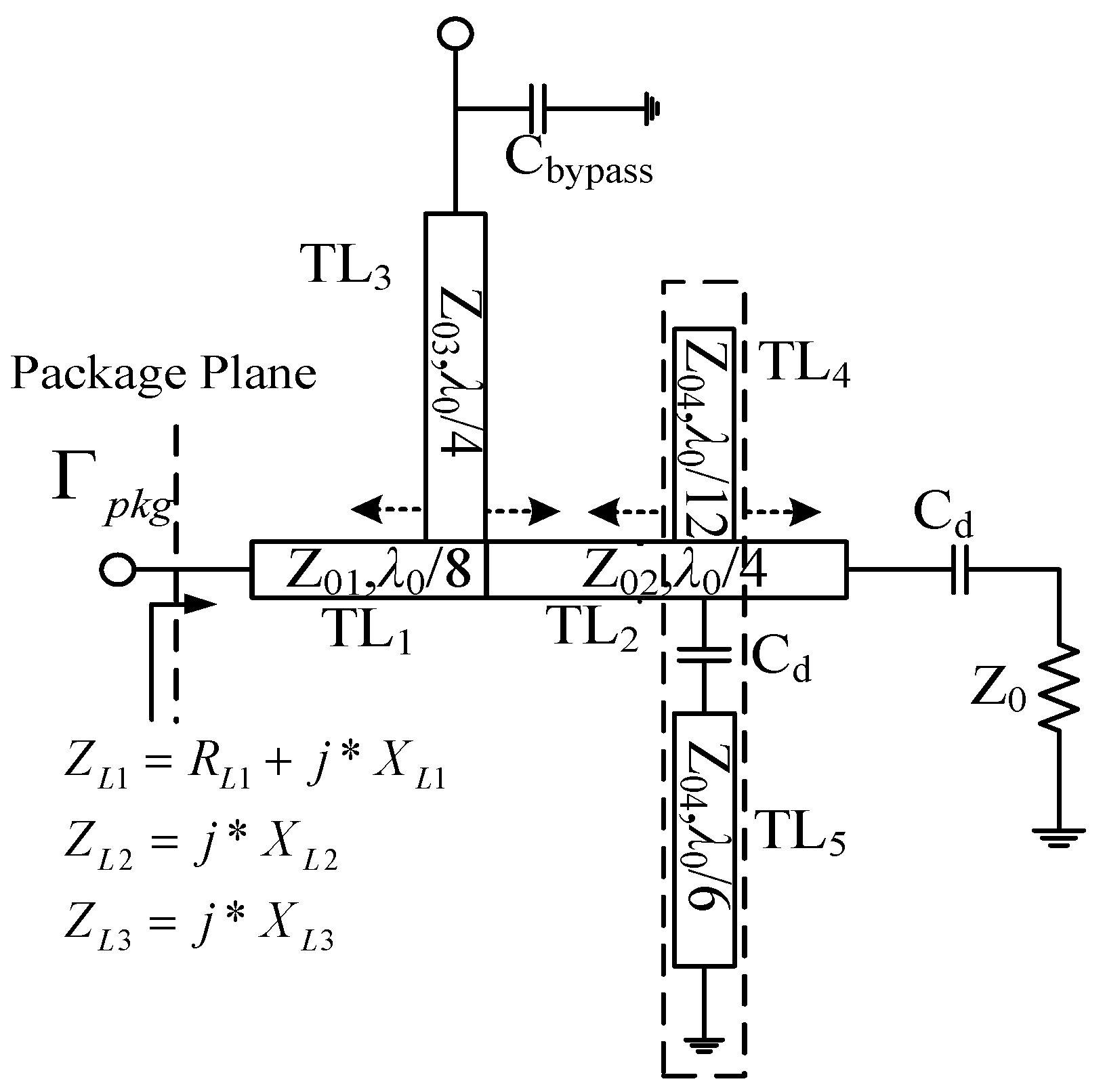
Based on the characteristics of fundamental and harmonic impedances, a method for controlling the first three harmonic impedances is proposed. Figure 2 presents the proposed topology.
A two-section impedance transformer—comprising two series-connected microstrips (TL1 and TL2)—matches the optimal fundamental impedance ZL1 at the package plane to a 50-Ω load. Three parallel microstrip stubs, integrated with the fundamental impedance matching circuit, realize the second- and third-order harmonic impedances. One stub also serves as the DC bias line. Consequently, the proposed harmonic-tuned network simultaneously and accurately compensates for the packaged transistor’s parasitic at both the second and third harmonics. The method’s implementation is structured into three key steps, detailed below.
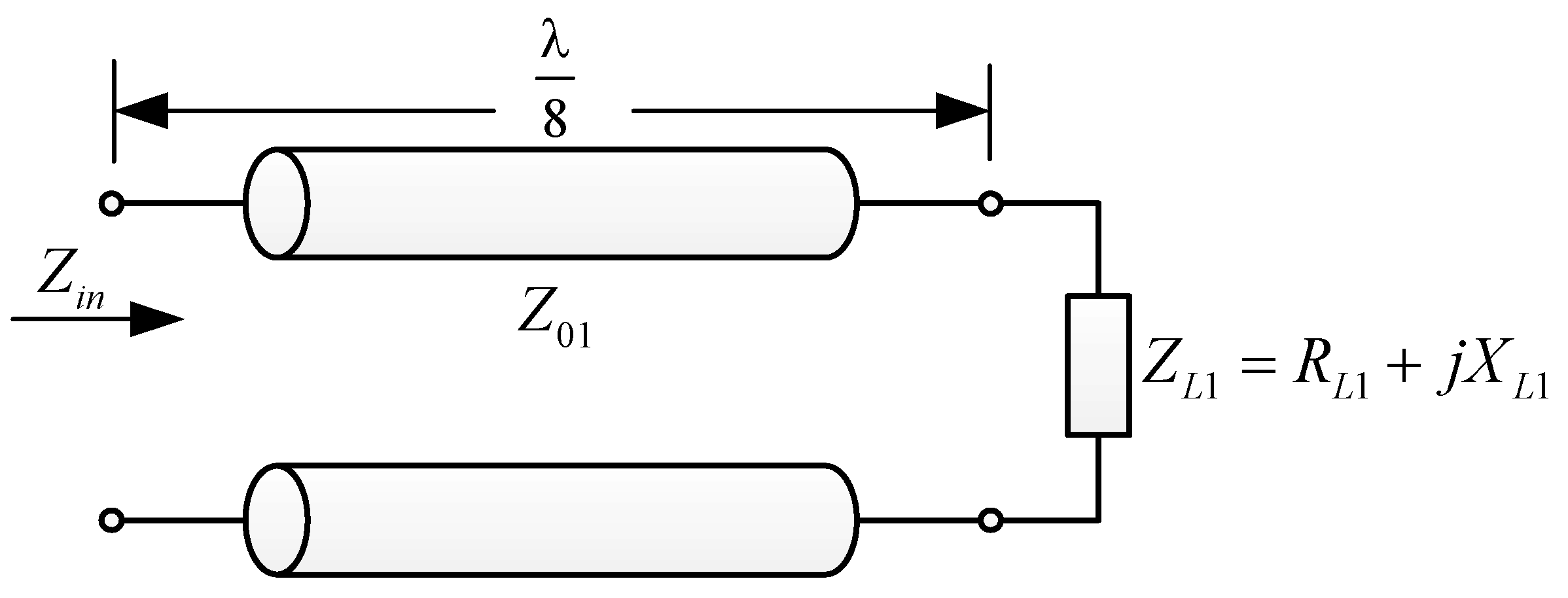
The first step matches the optimal fundamental impedance ZL1 at the package plane to a 50-Ω load. Transmission line TL1 is designed to convert the impedance from the package plane (ZL1 at f0) into a real resistance R1. Next, a quarter-wavelength (λ0/4, where λ0 is the wavelength at f0) transformer TL2 performs the transformation between R1 and the 50-Ω load Z0. This sets TL1’s electrical length to λ0/8. From [15], we can find R1 = |ZL1| × RL1/(|ZL1| − XL1). The schematic of the transformation of a λ/8 transmission line is depicted in Figure 3.
From Figure 3, we can obtain
Z i n = Z 01 Z L 1 + j Z 01 tan λ 8 β Z 01 + j Z L 1 tan λ 8 β ,
where
Z L 1 = R L 1 + j X L 1 .
Then we can obtain
Z i n = Z 01 ( R L 1 + j X L 1 ) + j Z 01 Z 01 + j ( R L 1 + j X L 1 ) ,
and then
Z i n = Z 01 R L 1 + j ( X L 1 + Z 01 ) ( Z 01 X L 1 ) + j R L 1 ;
Z i n = Z 01 R L 1 ( Z 01 X L 1 ) + Z 01 R L 1 ( X L 1 + Z 01 ) ( Z 01 X L 1 ) 2 + R L 1 2 + j Z 01 ( Z 01 + X L 1 ) ( Z 01 X L 1 ) R L 1 2 Z 01 ( Z 01 X L 1 ) 2 + R L 1 2 .
The imaginary part is
j Z 01 ( Z 01 + X L 1 ) ( Z 01 X L 1 ) R L 1 2 Z 01 ( Z 01 X L 1 ) 2 + R L 1 2 = 0 ,
So,
Z i n = R 1 = Z 01 R L 1 ( Z 01 X L 1 ) + Z 01 R L 1 ( X L 1 + Z 01 ) ( Z 01 X L 1 ) 2 + R L 1 2 = Z 01 R L 1 Z 01 X L 1 .
That means
R 1 = = Z L 1 R L 1 Z L 1 X L 1 .
Z 01 = Z L 1 = R L 1 2 + X L 1 2 .
Z 02 = R 1 Z 0 .
The second step involves determining the required second-harmonic impedance ZL2 at the package plane. ZL2 can be approximated as a pure imaginary value, as its real component is negligible. The electrical length of the DC biasing line TL3 is intentionally set to λ0/4 to present a short circuit for the second harmonic and an open circuit for the first and third harmonics at the junction with the main signal path. This short circuits’ condition at the second harmonic nullifies the circuit’s influence beyond the junction. Consequently, ZL2 is determined by adjusting the position of TL3, as illustrated in Figure 2.
The third step determines the required third-harmonic impedance ZL3 at the package plane. Like ZL2, ZL3 is similarly approximated as a pure imaginary value. An λ0/12 open stub (TL4) is connected in parallel to present a short circuit for the third harmonic at its junction with the main signal path. However, at the fundamental frequency, this shunt open stub introduces a residual reactance that compromises the fundamental frequency impedance matching established in Step 1. To mitigate this, a λ0/6 shunt short-circuited stub (TL5)—with the same characteristic impedance as TL4—is employed to compensate for the residual reactance at the fundamental frequency. A DC-blocking capacitor Cd is inserted between TL5 and the main path. Consequently, ZL3 is achieved by adjusting the position of the TL4–TL5 combination, as illustrated in Figure 2. Based on the above content, we can derive the specific values of ZL1, ZL2, and ZL3:
Z L 1 = Z 01 + j Z 01 2 ( Z 0 × j Z 04 3 3 2 + 6 3 Z 02 2 ( Z 0 + j Z 04 3 3 2 + 6 3 ) ) 1 + Z 01 Z 0 × j Z 04 3 3 2 + 6 3 Z 02 2 ( Z 0 + j Z 04 3 3 2 + 6 3 )
Z L 2 = Z 01 2 0 = +
Z L 3 = j Z 01 cos 3 4 π = j Z 01

3. Design and Verification

To validate the advantages of the proposed design methodology, a Cree GaN HEMT (model CGH40010F) (Newark, CA, USA)—comprising a bare CGH60015DE die and a Cree 440166 package—is employed to implement a Class-F−1 power amplifier. The package model is provided by the manufacturer, and the approximated equivalent circuit model of the device’s output parasitic network is detailed in [12]. The optimal first three harmonic impedances at the package plane (ZL1, ZL2, ZL3) are initially calculated using Equations (1) and (2).
Notably, device intrinsic parasitic effects are typically nonlinear (voltage-dependent), which degrades the accuracy of the theoretical model under high-power operation. To address this, the manufacturer’s nonlinear device model is incorporated to refine the calculation of the optimal first three harmonic impedances.
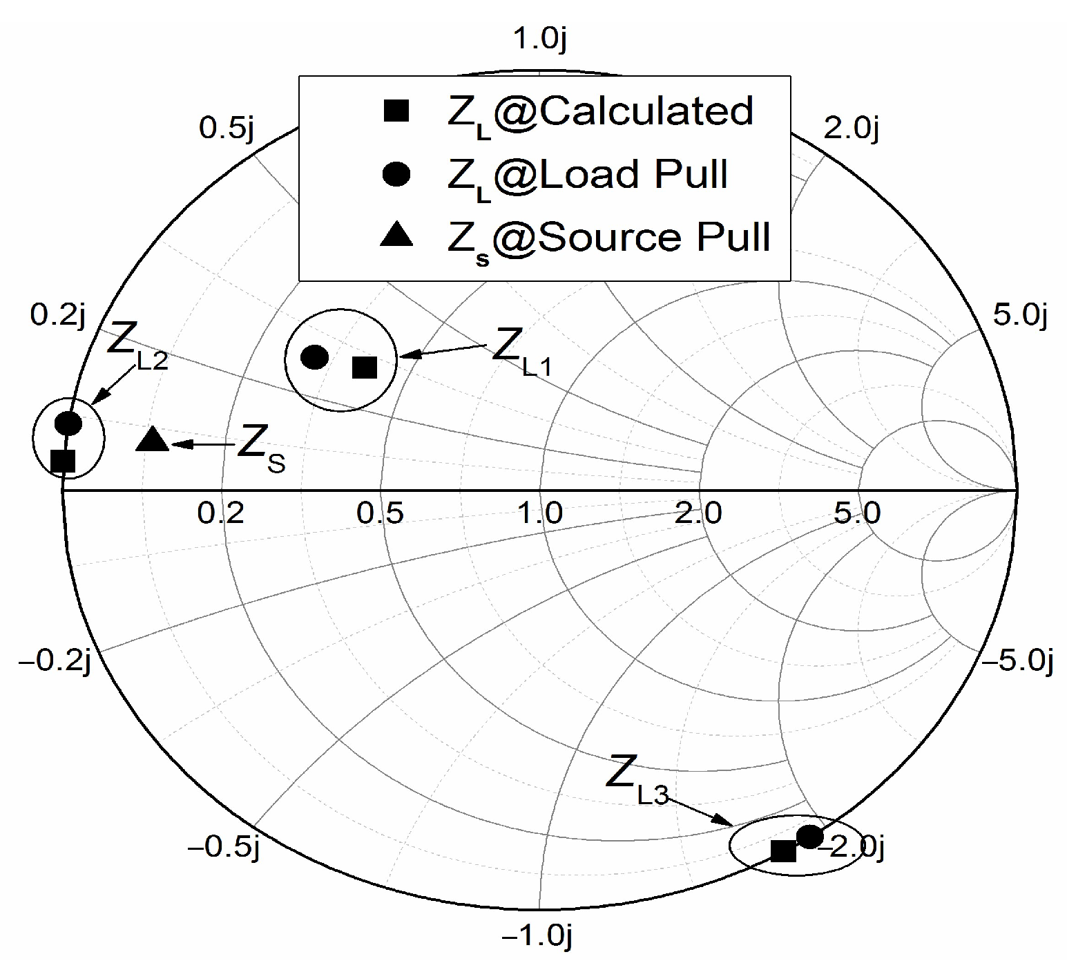
Load-pull simulations are then performed on the HEMT using the Keysight Advanced Design System (ADS) (Santa Clara, CA, USA), with the results from Equations (1) and (2) serving as initial guesses. Additionally, optimal source impedance (ZS) is extracted via source-pull simulations. The impedance distributions for these cases are plotted on the Smith Chart, as presented in Figure 4.
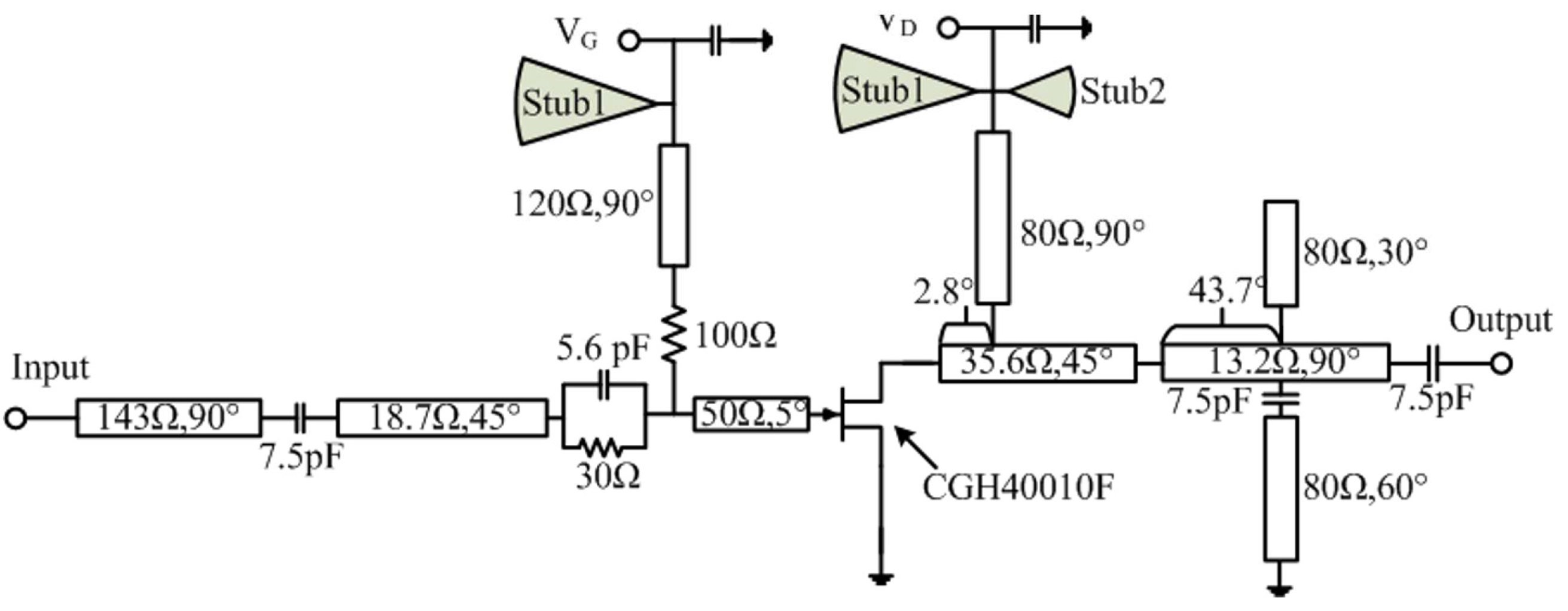
Figure 5 presents the complete schematic of the Class-F−1 power amplifier. An input matching network—implemented with a two-section impedance transformer—achieves complex–conjugate matching at the 2.5 GHz operating frequency to minimize insertion loss. The stability circuit comprises a series R-C network and a 100 Ω resistor in series with the gate bias line.
The output harmonic-tuned network follows the proposed methodology: a two-section impedance transformer converts the standard 50 Ω impedance to the optimal fundamental output impedance, while the positions of the λ0/4 biasing line and the TL4–TL5 combination are optimized along this transformer to achieve the target second- and third-order harmonic impedances.
Open radial stubs (Stub1 and Stub2), functioning as bypass capacitors in the biasing lines, provide short circuits for the fundamental and second harmonics. A capacitor of appropriate size is connected in parallel with Stub1/Stub2 to form a third-harmonic short circuit, simultaneously serving dual functions: DC power supply decoupling capacitor and third-harmonic bypass capacitor. It is particularly important to emphasize that in actual design, the resonance risk and engineering feasibility of this capacitor within the operating frequency band must be evaluated in advance. This supplementary design detail aims to provide a more comprehensive reference basis for subsequent engineering implementation. Finally, the designed Class-F−1 PA schematic is simulated and optimized in Keysight ADS.
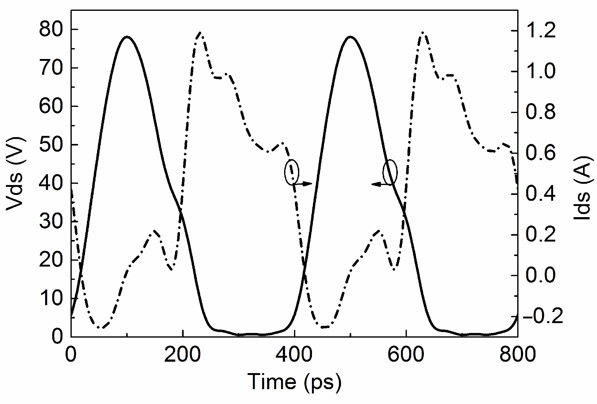
Figure 6 presents the simulated time-domain waveforms of the transistor’s drain current and voltage at the de-embedded intrinsic drain plane under Class-F−1 operation (2.5 GHz, 10 W output power). The drain voltage exhibits a near-half-sinusoidal shape, while the drain current approximates a square wave—consistent with ideal Class-F−1 behavior. Future work will expand the testing platform to include frequency domain characterization, thereby deepening our understanding of the underlying mechanisms.
The design and simulation of the passive network in this paper were both completed on the ADS platform, covering the entire process from schematic construction to parameter optimization and performance verification.

4. Results and Discussion

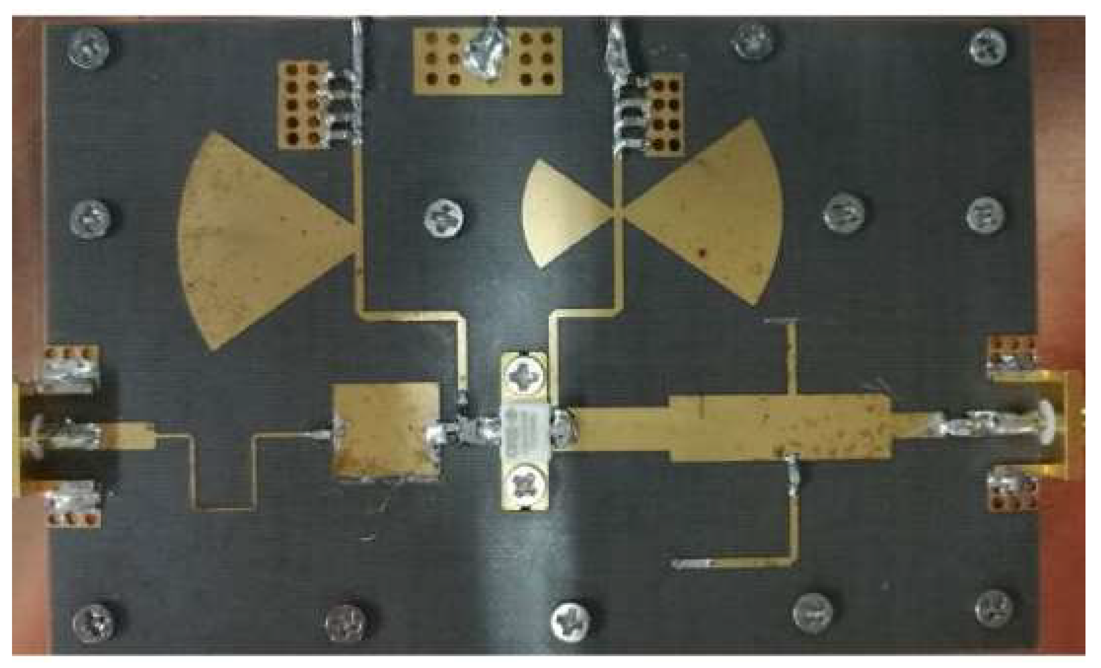
The Class-F−1 PA is fabricated on a Rogers 5880 (Chandler, AZ, USA) substrate (dielectric constant: εr = 2.2; thickness: 31 mils). Figure 7 presents a photograph of the fabricated PA mounted on a heat sink. The packaged transistor is subsequently placed into a metalized slot machined into the substrate, and the final assembly is mounted on a copper test fixture. Two SMA connectors interface with the PA, while two capacitors inserted in the DC path filter out low-frequency noise and DC offsets. The module measures 9 cm × 6.5 cm in total.
The device is biased at a drain voltage (Vd) of 28 V and a gate voltage (Vg) of −3 V. Note that the gate bias must be adjusted slightly to maintain consistent DC drain current between simulation and measurement—this accounts for variations in the 10-W HEMT’s threshold voltage and electron mobility.
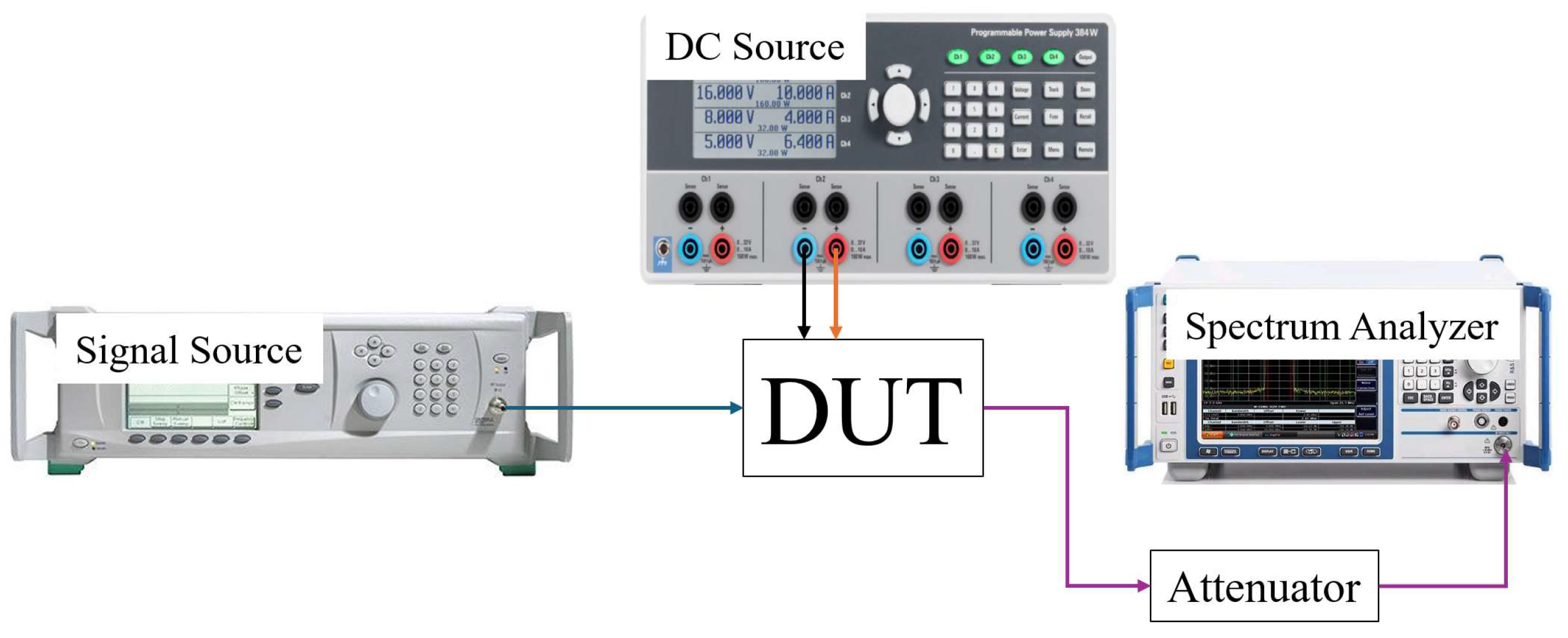
As shown in Figure 8, the test setup utilized a signal source, DC voltage source, spectrum analyzer, and attenuator. The attenuator was positioned at the front end of the spectrum analyzer to prevent excessive input power from damaging the analyzer. To enhance measurement accuracy, both the input and output ends were calibrated prior to testing, accounting for losses in cables and the attenuator.
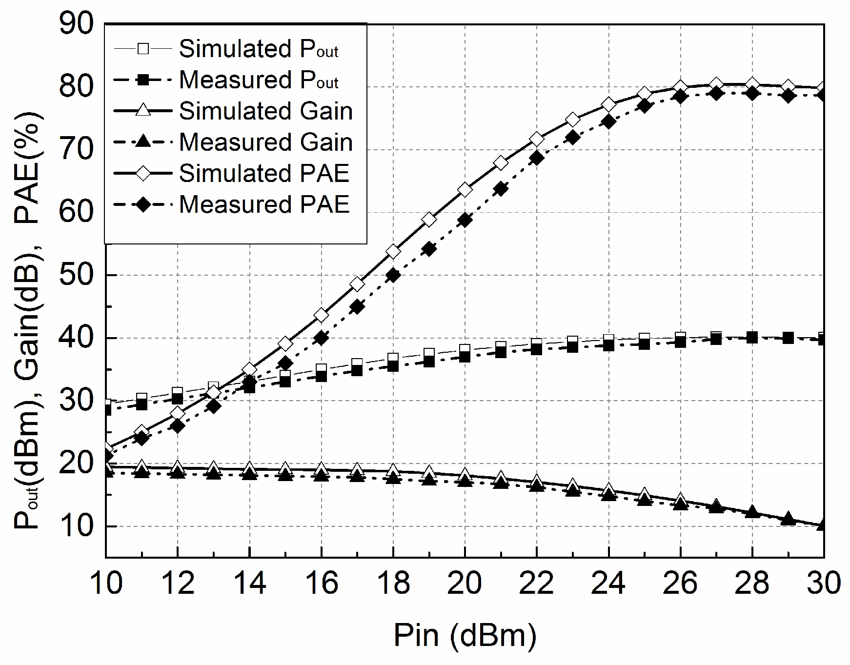
Figure 9 presents comparisons between simulated and measured output power (Pout), gain, and PAE of the Class-F−1 PA as the RF input power is swept from 10 to 30 dBm at 2.5 GHz. The amplifier achieves a peak drain efficiency of 81.6% and a maximum PAE of 79.8%, corresponding to a saturated output power of 40.2 dBm and a gain of 12.2 dB.
Minor discrepancies between simulated and measured results are observed across certain input power levels, attributed to limitations in the HEMT’s large-signal model accuracy, passive component fabrication tolerances, and substrate permittivity variations. Nevertheless, careful post-fabrication tuning of the matching transmission lines (TLs) can mitigate these discrepancies.
Table 1 compares the performance of the designed Class-F−1 PA to those of recently reported high-efficiency PAs designed using packaged devices. The proposed Class-F−1 PA products have excellent performance at the S-band. It is known that if the operating frequencies increase, the PAE will decrease. The proposed PA achieves a similar PAE as [13] at eight times the frequency [13], demonstrating that our approach is much more efficient. Moreover, our harmonic-tuned circuit achieves a more straightforward structure than those proposed in [9,12,16], respectively. Thus, a lower insertion loss has been introduced into the output of the PA, which results in a higher PAE.

5. Conclusions

This work proposes a simple microstrip harmonic-tuned load network for high-efficiency power amplifier (PA) design. Its efficacy is validated via a Class-F−1 PA implemented with a packaged GaN HEMT, achieving optimal harmonic loading (fundamental, second, and third) at the package plane. Experimental results demonstrate a peak PAE of 79.8% and saturated output power of 40.2 dBm at 2.5 GHz. Notably, this method offers a streamlined solution for harmonic tuning—surpassing traditional multi-line topologies in simplicity—while maintaining high performance. It is further applicable to other harmonic-tuned PA classes (e.g., Class-E/F, Class-FE), underscoring its broad design versatility.

Author Contributions

Conceptualization, G.Z. and S.Z.; methodology, G.Z. and S.Z.; software, G.Z. and S.Z.; validation, G.Z. and S.Z.; formal analysis, G.Z. and S.Z.; investigation, G.Z. and S.Z.; resources, G.Z. and S.Z.; data curation, G.Z. and S.Z.; writing—original draft preparation, G.Z. and S.Z.; writing—review and editing, G.Z. and S.Z.; visualization, G.Z. and S.Z.; supervision, S.Z.; project administration, S.Z.; funding acquisition, S.Z. All authors have read and agreed to the published version of the manuscript.

Funding

This work was supported by the Natural Science Foundation of Zhongyuan University of Technology under Grant No. K2025ZD009 and the General Program of Henan Provincial Natural Science Foundation under Grant No. 252300421892.

Data Availability Statement

The data that support the findings of this study are available from the corresponding author upon reasonable request.

Acknowledgments

The author would like to express sincere gratitude to Ma Jianguo and Wang Caixia for their contributions to and guidance through this research. Special thanks go to Wang Caixia for her full support in the primary work of this paper. We also extend our appreciation to the R&D Team for Contactless Receipt Technology for their support.

Conflicts of Interest

The authors declare no conflict of interest.

References

  1. Ren, M.; Gao, R.; Liu, S.; Li, M.; Shi, W.; Dai, Z.; Chen, S.; Pang, J. Design of Wideband Doherty Power Amplifier Using Inverse Continuous Class-F Mode. IEEE Trans. Circuits Syst. II Express Briefs 2024, 71, 4176–4180. [Google Scholar] [CrossRef]
  2. Ghanaatian, A.; Abrishamifar, A.; Rahmati, A.; Alizadeh, A. A 15-W X-Band Inverse Class-F GaN Power Amplifier with Second-Harmonic Input Tuning. IEEE Microw. Wirel. Technol. Lett. 2023, 71, 1317–1320. [Google Scholar] [CrossRef]
  3. Zahid, H.; Kamran Saleem, M.; Maalik, A.; Ikram, M. Hybrid Load-Pull and Nonlinear Embedding Approach for High-Efficiency GaN Class-F/F−1 Power Amplifier Design in Satellite Applications. IEEE Access 2025, 13, 173768–173789. [Google Scholar] [CrossRef]
  4. Mi, J.; Fan, R.; Yan, L.; Feng, Y.; Liu, C. Design of a High-Power and High-Efficiency GaN-HEMT VCO Based on an Inverse Class-F Amplifier. IEEE Microw. Wirel. Technol. Lett. 2025, 35, 241–244. [Google Scholar] [CrossRef]
  5. Shang, Y.-H.; Chuang, K.-Y.; Lin, H.-C.; Chang, Y.-C.; Chang, D.-C.; Hsu, S.S.H. A Continuous-Mode Class-F−1 X -Band Gan Mmic Power Amplifier with a 29.7. In Proceedings of the 2025 IEEE/MTT-S International Microwave Symposium-IMS 2025, San Francisco, CA, USA, 15–20 June 2025. [Google Scholar]
  6. Jiang, H.; Li, H.; Liu, F. Design of a High-Efficiency Multi-Octave Continuous Class-GF−1 Power Amplifier with In-Band Flexible Operation. In Proceedings of the 2025 International Conference on Microwave and Millimeter Wave Technology (ICMMT), Xi’an, China, 19–22 May 2025. [Google Scholar]
  7. Young, Y.W.; Yang, Y.; Kim, B. Analysis and experiments for high-efficiency class-F and inverse class-F power amplifiers. IEEE Trans. Microw. Theory Tech. 2006, 54, 1969–1974. [Google Scholar] [CrossRef]
  8. Cheng, Q.F.; Fu, H.-P.; Zhu, S.-K.; Wu, H.-F.; Ma, J.-G. High-efficiency GaN Class-F/Class-F−1 power amplifiers with distributed L-shaped parasitic-compensation circuit. Microw. Opt. Technol. Lett. 2015, 57, 2441–2445. [Google Scholar] [CrossRef]
  9. Lee, Y.; Lee, M.; Jeong, Y. High-Efficiency Class-F GaN HEMT Amplifier with Simple Parasitic-Compensation Circuit. IEEE Microw. Wirel. Compon. Lett. 2008, 18, 55–57. [Google Scholar] [CrossRef]
  10. Chen, S.; Xue, Q. A Class-F Power Amplifier with CMRC. IEEE Microw. Wirel. Compon. Lett. 2011, 21, 31–33. [Google Scholar] [CrossRef]
  11. Hayati, M.; Sheikhi, A.; Grebennikov, A. Class-F Power Amplifier with High Power Added Efficiency Using Bowtie-Shaped Harmonic Control Circuit. IEEE Microw. Wirel. Compon. Lett. 2015, 25, 133–135. [Google Scholar] [CrossRef]
  12. Hayati, M.; Shama, F. A high-efficiency narrow-band Class-F power amplifier integrated with a microstrip suppressing cell. Analog Integr. Circuits Signal Process. 2017, 90, 351–359. [Google Scholar] [CrossRef]
  13. Beltran, R.A. Class-F and inverse class-F power amplifier loading networks design based upon transmission zeros. In Proceedings of the 2014 IEEE MTT-S International Microwave Symposium (IMS2014), Tampa, FL, USA, 1–6 June 2014. [Google Scholar]
  14. Ding, Y.; Guo, Y.-X.; Liu, F. A new method to design high efficiency power amplifier using dual-band transformer. In Proceedings of the Asia-Pacific Microwave Conference 2011, Melbourne, Australia, 5–8 December 2011. [Google Scholar]
  15. Steinbrecher, D.H. An Interesting Impedance Matching Network. IEEE Trans. Microw. Theory Tech. 1967, 15, 382. [Google Scholar] [CrossRef]
  16. Cheng, Q.F.; Fu, H.P.; Zhu, Y.Y.; Ma, J.-G. High-efficiency parallel-circuit class-E power amplifier with distributed T-shaped compensation circuit. IEICE Electron. Express 2016, 13, 20160570. [Google Scholar] [CrossRef]
  17. Hussen, L.; Wei, M.-D.; Negra, R. High-Efficient Inverse Class-F Power Amplifier Utilising Nonuniform Transmission Lines for Wireless Power Transfer. In Proceedings of the 2024 31st IEEE International Conference on Electronics, Circuits and Systems (ICECS), Nancy, France, 18–20 November 2024. [Google Scholar]
  18. Piacibello, A.; Zhang, Z.; Camarchia, V. Continuous Inverse Class-F GaN Power Amplifier with 70% Efficiency over 1.4–2 GHz Bandwidth. In Proceedings of the 2023 IEEE Topical Conference on RF/Microwave Power Amplifiers for Radio and Wireless Applications, Las Vegas, NV, USA, 22–25 January 2023. [Google Scholar]
  19. Yang, S.; Dong, Q.; Huang, W.; Jiang, X.; Wei, K.; Liu, X.; Luo, W. A High-Efficiency Inverse Class-F GaN MMIC Power Amplifier with Compact Output Matching Network. IEEE Trans. Circuits Syst. II Express Briefs 2023, 70, 3767–3771. [Google Scholar] [CrossRef]
  20. Atilla, C.D.; Alsaedi, M.O.H.; Alsaadi, H.A.J. Design Continues Mode Inverse Class-F Power Amplifier. In Proceedings of the 2023 International Conference on Engineering and Emerging Technologies (ICEET), Istanbul, Turkey, 27–28 October 2023. [Google Scholar]
  21. Kim, B.; Oh, J. Dual-Band Continuous Class-F−1 Power Amplifier with Second-Harmonic Suppression for Harmonic Radar Systems. IEEE Access 2024, 12, 62358–62364. [Google Scholar] [CrossRef]
  22. Liu, W.; Liu, Q.; Du, G.; Li, G.; Cheng, D. Dual-Band High-Efficiency Power Amplifier Based on a Series of Inverse Continuous Modes with Second-Harmonic Control. IEEE Microw. Wirel. Technol. Lett. 2023, 33, 1199–1202. [Google Scholar] [CrossRef]
Figure 1. Active device harmonic impedances (the Class F−1 is taken as an example).
Electronics 14 04767 g001
Figure 2. Proposed harmonic-tuned matching network using microstrips.
Electronics 14 04767 g002
Figure 3. Schematic of impedance transformation with a λ / 8 transmission line.
Electronics 14 04767 g003
Figure 4. Optimal impedances at the package plane.
Electronics 14 04767 g004
Figure 5. Schematic of the designed Class-F−1 PA using the proposed method.
Electronics 14 04767 g005
Figure 6. De-embedded intrinsic drain waveforms of the voltage and current from ADS simulation.
Electronics 14 04767 g006
Figure 7. Photograph of the fabricated GaN HEMT Class-F−1 PA.
Electronics 14 04767 g007
Figure 8. Schematic diagram of measurement setup.
Electronics 14 04767 g008
Figure 9. Simulated and measured output power, gain, and PAE of the designed Class-F−1 PA.
Electronics 14 04767 g009
Table 1. Performance comparison of various high-efficiency PAs.
ReferenceModeFrequency (GHz)Pout (dBm)PAE (%)Gain (dB)
[9]-2018Class-F2.1440.270.912.2
[12]-2017Class-F1.823.473.517.5
[13]-2014Class-F−10.342.3779 *11.37
[16]-2016Class-E2.940.272.212.2
[1]-2024Class-F−10.7–1.142.6–43.366.0 *–74.6 *13.5–16
[17]-2024Class-F−12.3–2.5536.7672.713.4
[18]-2023Class-F−11.4–2.0407013
[19]-2023Class-F−13.038.464.510.3
[20]-2023Class-F−11.5–2.040–40.170.416
[21]-2024Class-F−12.3/3.3540.34/41.972.6/59.512.9/8.8
[22]-2023Class-F−13.37–3.5240–41.265–76.28.8–11.2
[6]-2025Class-GF−10.6–2.839.8–42.565 *–74 *9.8–13.28
This workClass-F−12.540.279.812.2
* Drain efficiency.
Disclaimer/Publisher’s Note: The statements, opinions and data contained in all publications are solely those of the individual author(s) and contributor(s) and not of MDPI and/or the editor(s). MDPI and/or the editor(s) disclaim responsibility for any injury to people or property resulting from any ideas, methods, instructions or products referred to in the content.