Abstract
This paper proposes a design method for a broadband power amplifier (PA) capable of concurrent dual-band operation at any two distinct frequency points within its operational bandwidth. The concurrent performances of a broadband PA versus the variation in baseband impedance are analyzed. To enhance the concurrent efficiency, the baseband impedance of the broadband PA is controlled over a wide baseband frequency range through a novel control network. A 1.75–2.25 GHz PA is designed and fabricated. Under a single-tone continuous-wave (CW) signal excitation, the fabricated PA achieves 40.9–42.0 dBm maximum output power and 63.3–77.3% drain efficiency (DE) in its operational bandwidth. When operating under a balanced concurrent mode, its measured output power exceeds 39.6 dBm and its DE surpasses 66.2% in the tone spacing range of 0–500 MHz.
1. Introduction
Concurrent dual-band power amplifiers (DB-PAs) can simultaneously process signals from two frequency bands, avoiding the switching delay of traditional single-band power amplifiers (PAs) [1]. This leads to the improvement in the spectrum utilization of wireless communication systems. Moreover, the number of RF front-end modules can be reduced by integrating concurrent dual-band PAs, reducing system complexity and cost [2,3]. Given these advantages, the concurrent DB-PA has emerged as a pivotal enabler for next-generation wireless systems. Its deployment will accelerate exponentially with the global rollout of 5G/6G networks and IoT ecosystems, where dynamic spectrum access and multi-band coexistence are paramount. Consequently, research on concurrent dual-band PA remains a critical focus area in modern RF engineering [4,5].
In recent years, many articles on the realization of DB-PAs have emerged one after another [6,7]. In [7], a stop-band filter was integrated into the output matching network (OMN) of a high-efficiency DB-PA. This DB-PA obtains saturation drain efficiencies (DEs) of 68.2–75.7% and 68.9–76.3% over 1.95–2.4 GHz and 2.65–3.1 GHz frequency bands, respectively. In [8], the authors proposed a novel dual-band harmonic control network to enhance the efficiency of a DB-PA. The DB-PA in [8] achieved DEs of 78.5% and 76.7% at 1.84 and 3.22 GHz, respectively. Notice that most dual-band PAs focus on how to improve the efficiency at two frequency points, while ignoring the concurrent performance.
Unlike single-tone signal excitation, a PA has a completely different behavior under a concurrent two-tone signal excitation. In [9,10], the behavior of a PA under concurrent two-tone signal excitation was thoroughly examined, revealing that controlling inter-modulation impedances is crucial for improving concurrent performance. Moreover, it is indicated in [11] that concurrent class-J PA demonstrates significantly higher efficiency compared to its concurrent dual-band class-B counterpart. Additionally, the performance of a concurrent DB-PA is strongly influenced by the reactive component of the load at the inter-modulation frequency, as highlighted in [12]. According to the analyses conducted in [12,13,14], the baseband load impedance is identified as the primary factor contributing to performance degradation in concurrent DB-PAs. Consequently, it is essential to consider the baseband impedance when designing a concurrent DB-PA. In [15,16,17,18,19], concurrent class-B, -B/J and -F DB-PAs were analyzed and designed with meticulous control over the baseband impedance. In [15], the implemented concurrent DB-PA operates at 2.7/3.5 GHz. It achieves a concurrent DE of 62.6%. In [16], an 1.9/2.35 GHz concurrent DB-PA under class-B/J mode was implemented, achieving a concurrent DE of 60.4%. In [17], by controlling the baseband impedance, a highly efficient concurrent dual-band class-F PA was constructed. This DB-PA achieved a concurrent DE 60% when the concurrent power is 40 dBm.
It is important to note that the concurrent dual-band PAs mentioned above primarily operate at two fixed frequency points, which restricts the flexibility of dual-band applications. Indeed, there is a strong desire for broadband PAs capable of supporting flexible concurrent operation across their entire operational bandwidth. This implies that the broadband PA should maintain high concurrent performance when operating at any two frequencies within its bandwidth. Achieving this necessitates precise control of the baseband impedance from zero up to the frequency equivalent to the RF bandwidth of the broadband PA. In [14], a broadband PA was developed to operate within the 1.8–2.2 GHz frequency band, enabling concurrent operation with a tone spacing ranging from 0 to 400 MHz. Meanwhile, in [18], a broadband class-F2 PA was implemented, offering flexible concurrent operation within the same 1.8–2.2 GHz frequency range. Measurement results showed that this class-F2 PA achieved a concurrent output power between 40.0 and 40.6 dBm and a DE ranging from 60.0% to 64.0% over 0–400 MHz tone spacing.
Based on the previous papers, this work first offers a comprehensive analysis on the performances of a concurrent DB-DPA. Based on an ideal assumption, the concurrent performances of a class-B PA are expressed as functions of the baseband impedance. Theoretical analysis indicates that the real part of the baseband impedance has a more severer effect on the concurrent performance when compared to the imaginary part. Subsequently, a baseband impedance control method is introduced to design a broadband PA that supports flexible concurrent operation within the 1.75–2.25 GHz frequency range. When the fabricated PA is measured using a balanced two-tone continuous-wave (CW) signal centered at 2.0 GHz, it delivers a concurrent output power spanning from 39.6 dBm to 40.2 dBm and attains a concurrent DE changing from 66.2% to 68.8% over a tone spacing that extends from 0 to 500 MHz.
2. Broadband PA with Baseband Impedance Control
This section gives an analysis of how the performance of a concurrent DB-PA varies with baseband impedance. Furthermore, a baseband control method is introduced to optimize and enhance the concurrent efficiency of a broadband PA.
2.1. Concurrent Dual-Band PA with Non-Zero Baseband Impedance
The block diagram of a broadband PA operating under concurrent two-tone CW signal excitation is depicted in Figure 1. Here, we assume the transistor operates in class-B mode and focus solely on the baseband and fundamental frequency components. The transistor within the broadband PA is considered as an ideal voltage-controlled current source accompanied by intrinsic elements. The PA is supplied with a drain voltage denoted as . At the transistor internal plane, the drain-to-source voltage and current are represented by and , respectively.

Figure 1.
Block diagram of a broadband PA under concurrent two-tone signal excitation.
To ensure the PA maintains high performance across the desired bandwidth, the fundamental load impedance is configured to , which corresponds to the optimal load impedance for a class-B PA at the transistor internal plane. As per the analysis presented in [20], under an excitation of a balanced concurrent two-tone CW signal, the fundamental and DC components of a DB-PA can be mathematically expressed as
where and are the fundamental and DC components of . And is the DC components of and can be derived using
This equation means the baseband impedance will affect the drain voltage swing of the transistor, leading to a variation in the concurrent performance.
Using (1)–(3), the maximum output power of a broadband PA under balanced concurrent mode can be calculated using
And the DC power of the PA at the saturation power level is
Therefore, the saturation concurrent DE of the PA is
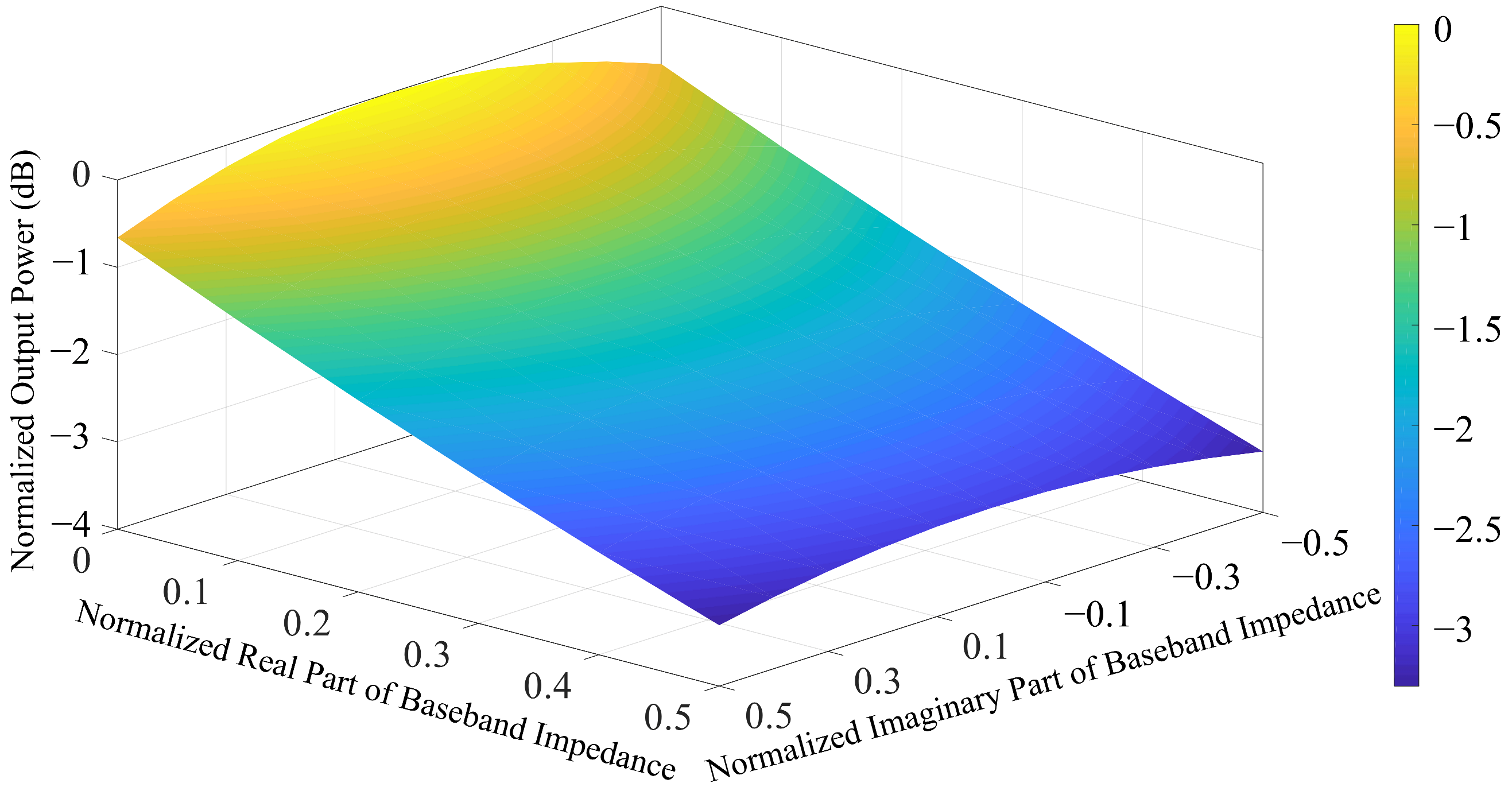
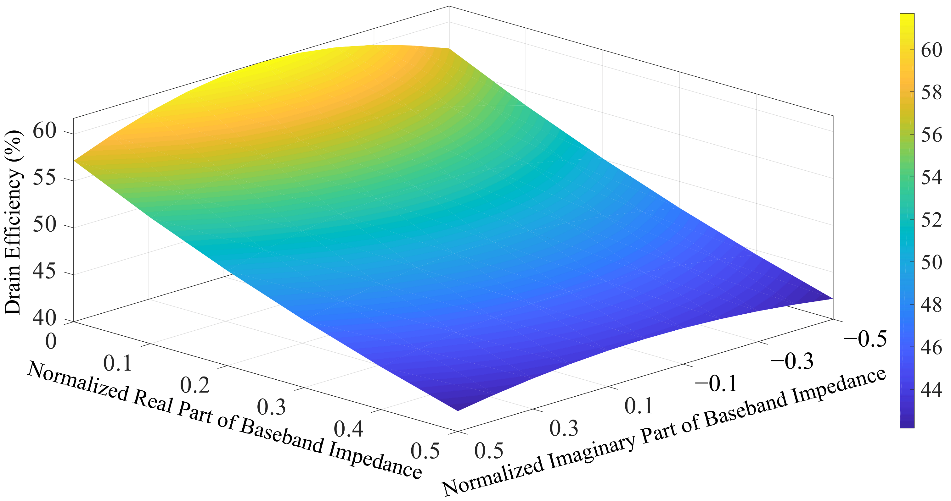
Using (4), the normalized output power of a class-B PA versus the variation in the real and imaginary parts of the baseband impedance is depicted in Figure 2. Note that the output power is normalized to the output power level when the baseband impedance is zero. As depicted in Figure 2, the normalized output power decreases as the real part increases or as the imaginary part deviates from zero. Using (6), Figure 3 depicts the concurrent DE of a class-B PA with respect to the real and imaginary parts of the baseband impedance. From Figure 3, the concurrent DE of a class-B PA also decreases as the real part increases or as the imaginary part deviates from zero. From Figure 2 and Figure 3, when equals 0.5, the concurrent DE of a class-B PA drops from 61.7% to 43.9% and the concurrent output power decreases by 3 dB. Moreover, when compared to the real part of the baseband impedance, the imaginary part exerts a relatively minor effect on the concurrent performances, as shown in Figure 2 and Figure 3. Consequently, when designing a broadband PA, we prefer the baseband impedance to vary along the edge of the Smith chart.
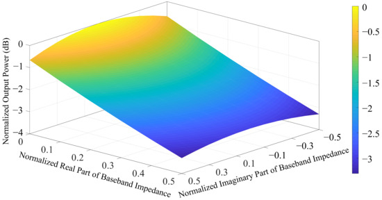
Figure 2.
Normalized output power of a class-B PA under balanced concurrent mode versus the real and imaginary parts of the baseband impedance.

Figure 3.
Drain efficiency of a class-B PA under balanced concurrent mode versus the real and imaginary parts of the baseband impedance.
2.2. Broadband PA with Baseband Impedance Control for Concurrent Operation
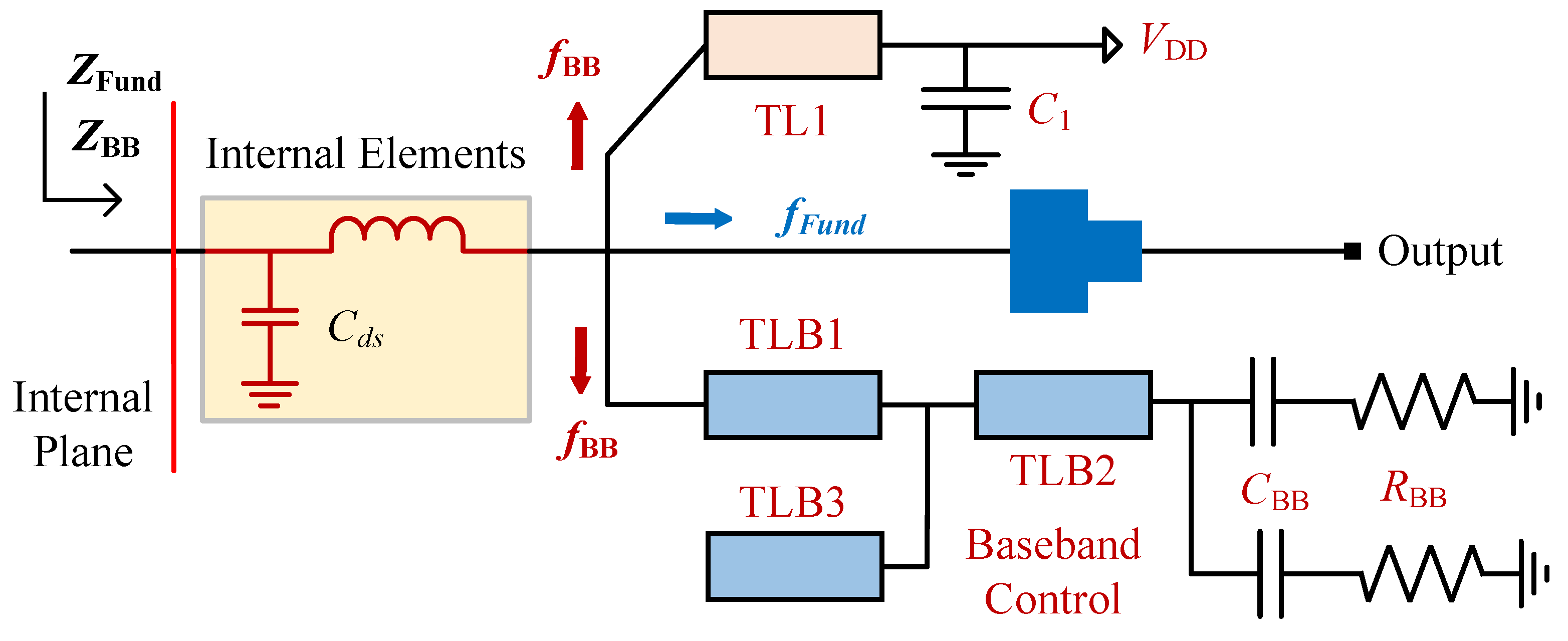
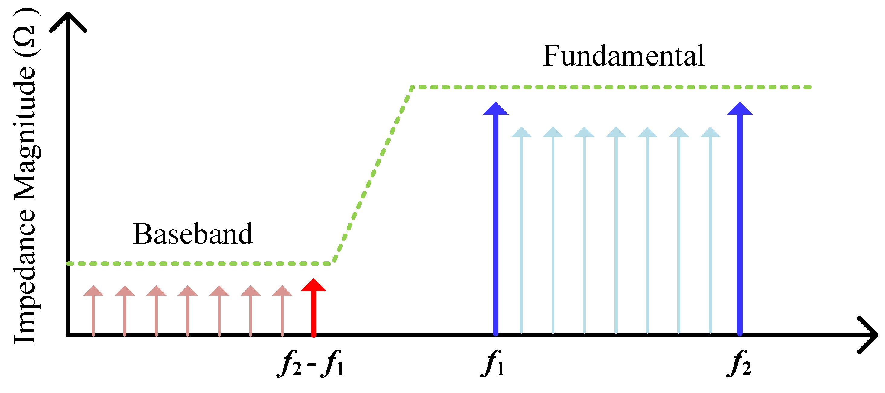
According to the theoretical analysis, the baseband impedance should be controlled to be as small as possible, especially for the real part. Otherwise, the concurrent performance of a PA will be degraded. In this paper, a broadband PA with baseband impedance control is proposed for concurrent operation. The block diagram of the proposed PA is illustrated in Figure 4. The baseband impedance is controlled by a low-pass filter which is connected in series with a R-C circuit. Meanwhile, the bias circuit is also utilized to control the baseband impedance. As shown in Figure 5, the low-pass filter consists of three transmission lines TLB1, TLB2, and TLB3. The R-C circuit and provide the main path with a low impedance over a wide baseband frequency range. Meanwhile, the whole OMN provides the active device with an optimal load impedance at the transistor internal plane over the whole fundamental frequency range, as shown in Figure 6.

Figure 4.
Block diagram of the proposed broadband with baseband impedance control.
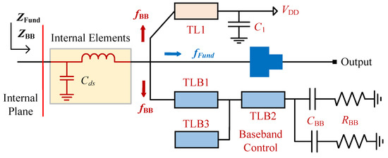
Figure 5.
Block diagram of the OMN for the proposed broadband PA.
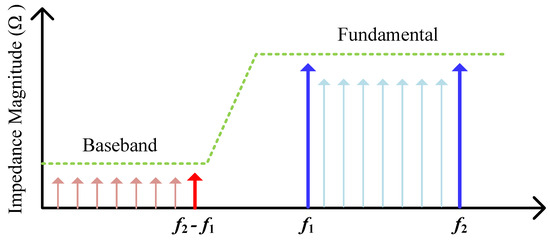
Figure 6.
Theoretical load impedance of the proposed broadband PA.
3. Design and Simulation Results
Based on the structure shown in Figure 4, a broadband PA is designed in this part for concurrent operation. And the simulation results of the designed PA are also presented in this part.
3.1. Broadband PA Design
The broadband PA is designed based on the CG2H40010F transistor from Wolfspeed with a gate voltage of −3.0 V and a drain voltage of 28 V. The optimal load impedance of the utilized transistor at the internal plane is set to = 36 . The expected frequency range is 1.75–2.25 GHz (500 MHz). The 4350B substrate form Rogers corporation is utilized when designing the PA. The thickness of the substrate is 20 mil.
The design method of the broadband PA is the same as in [18]. The main difference is the design of the baseband impedance control circuit. In this design, the parameters of the baseband impedance control circuit for the broadband PA are optimized using optimization function in the Advanced Design System (ADS). Figure 7 shows the schematic of the implemented PA. Meanwhile, the values of the utilized passive elements are also given in Figure 7.

Figure 7.
Schematic of the designed broadband PA.
3.2. Single-Tone Simulation Results
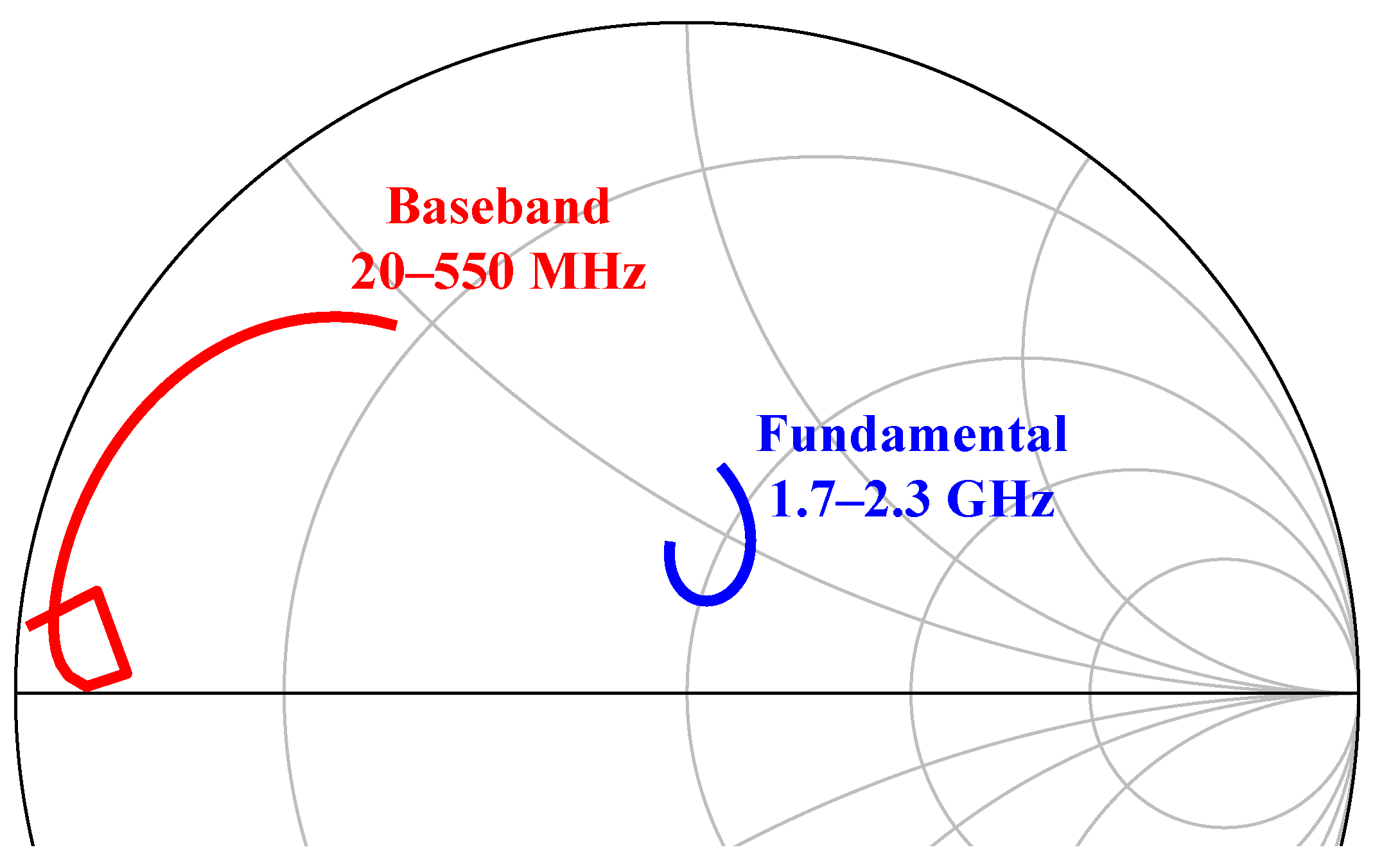
Firstly, a single-tone CW signal is utilized to simulate the designed PA. The simulated intrinsic load trajectories of the designed broadband concurrent PA is shown in Figure 8. In this figure, the reference impedance utilized for the Smith chart is 36 . As observed from Figure 8, the fundamental impedance of the PA closely approximates the optimal load impedance. Additionally, over the frequency range of 0–500 MHz, the transistor perceives a relatively low baseband impedance.

Figure 8.
Simulated intrinsic Load trajectories of the designed broadband concurrent PA.
The simulated DE and gain of the broadband PA are illustrated in Figure 9. The designed PA is capable of delivering a maximum output power of 41.3–41.9 dBm over 1.75–2.25 GHz. And the designed PA achieves a saturation DE between 73.1% and 78.5%, along with a gain spanning from 15.1 dB to 15.9 dB, across the frequency band of 1.75 GHz to 2.25 GHz.

Figure 9.
Simulated DE and gain of the designed PA under the excitation of a single-tone CW signal.
3.3. Concurrent Two-Tone Simulation Results
A two-tone CW signal is also utilized to simulate the broadband PA. The two-tone CW signal is centered at 2.0 GHz. Under a balanced concurrent mode, the simulated DE and gain of the broadband PA are depicted in Figure 10 when the tone spacing is varied incrementally from 0 MHz up to 500 MHz. The maximum output power of the broadband concurrent PA is larger than 39.9 dBm. And the concurrent DE is larger than 69%. Furthermore, at the saturation power level, the designed PA also achieves a concurrent gain exceeding 13.9 dB, as shown in Figure 11.
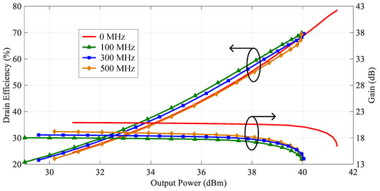
Figure 10.
Simulated concurrent DE and gain versus the output power of the designed PA when the tone spacing is swept from 0 to 500 MHz.
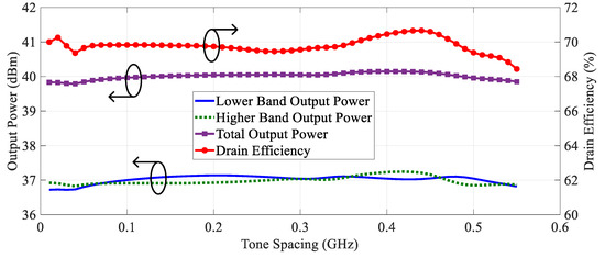
Figure 11.
Simulated concurrent DE and output power of the designed PA at the saturation power level versus tone spacing.
The simulated maximum concurrent output power and DE as a function of tone spacing are presented in Figure 11. The designed PA achieves a maximum concurrent output power changing from 39.8 dBm to 40.2 dBm over a 500 MHz tone spacing. The simulated maximum concurrent DE of the designed PA falls between 69.4% and 70.7% in the same tone spacing range. Moreover, Figure 11 also illustrates the simulated output power of the designed PA across both the lower and higher frequency bands. In the upper frequency band, the maximum output power of the PA ranges from 36.8 dBm to 37.2 dBm. And within the lower frequency band, the peak output power changes from 36.7 dBm to 37.1 dBm.
4. Measurement Results
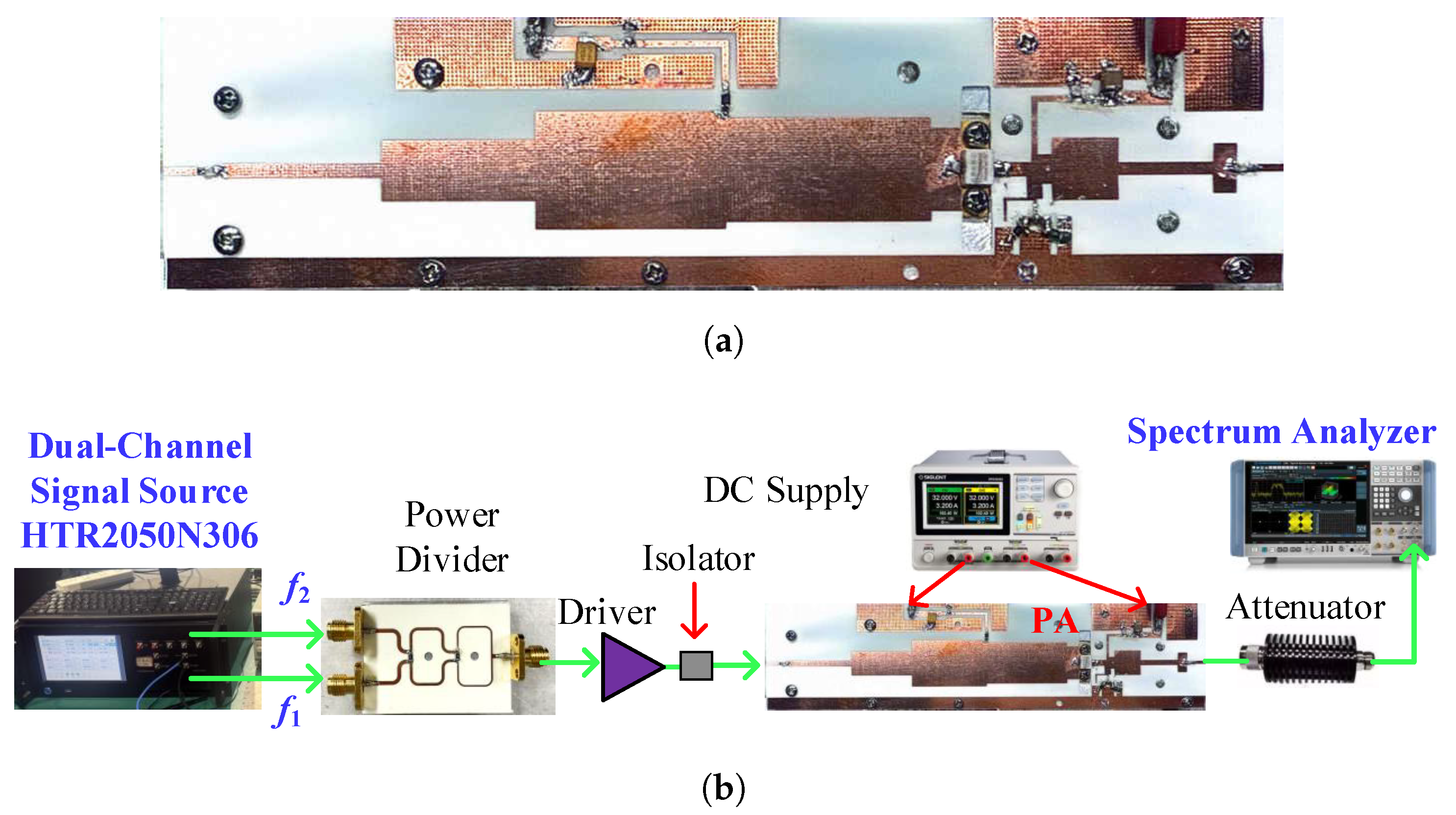
Figure 12a displays the photograph of the manufactured broadband PA. The testing setup for the broadband concurrent PA is illustrated in Figure 12b. Two signals at distinct frequency points are generated using a dual-channel signal generator. These signals are then combined together using a 1:1 power divider. Subsequently, the combined concurrent signal is directed to a driver to ensure sufficient power is delivered to the fabricated PA. To maintain a stable experimental environment, an isolator is placed between the driver and the fabricated PA. Both the driver and the fabricated PA are powered by a DC supply. After passing through a 40 dB attenuator, the output power of the fabricated PA is collected by a spectrum analyzer. During the testing, the drain and gate voltages of the PA are set to 28 V and −2.8 V, respectively.

Figure 12.
(a) Photograph of the fabricated broadband PA and (b) its test bench.
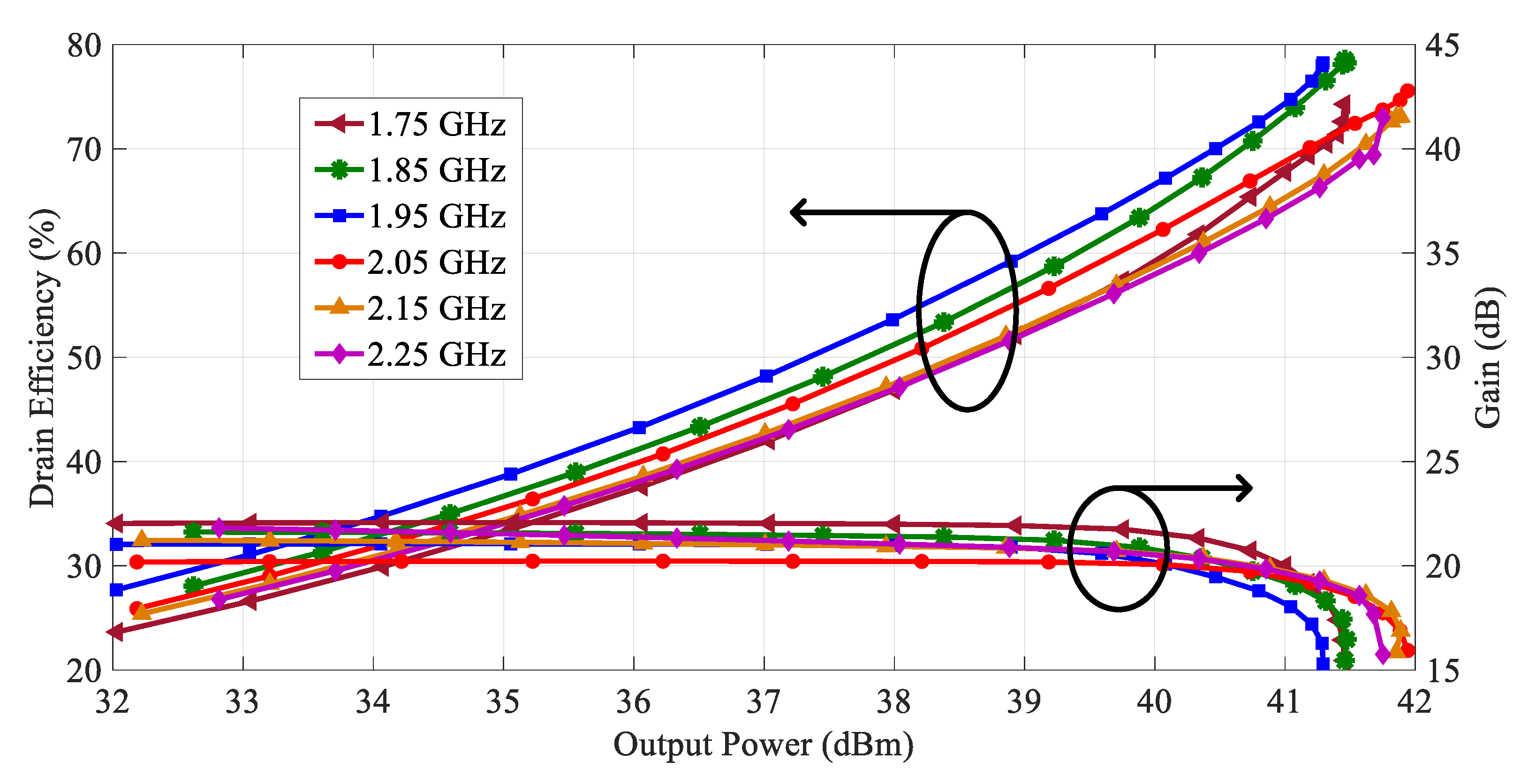
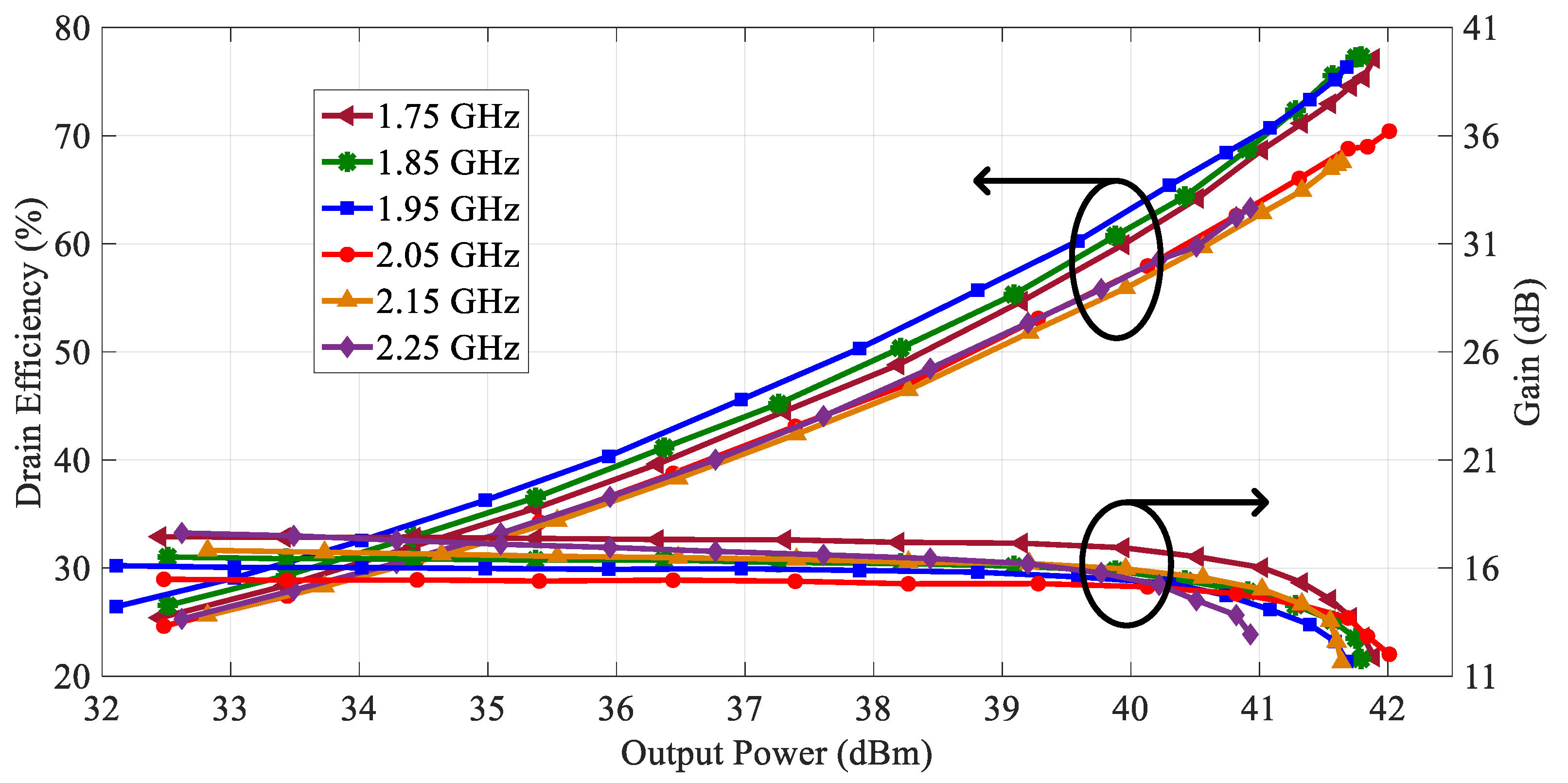
When tested by a single-tone CW signal, the measured DE and gain of the PA with respect to output power and frequency are depicted in Figure 13. The results demonstrate that the fabricated PA attains an output power ranging from 40.9 dBm to 42.0 dBm and achieves a DE between 63.3% and 77.3% at the saturation power level within the frequency range of 1.75 GHz to 2.25 GHz. Furthermore, the measured gain of the fabricated PA falls within the range of 11.7 dB to 12.9 dB.

Figure 13.
Measured DEs and gains versus output power of the fabricated PA at different frequency points.
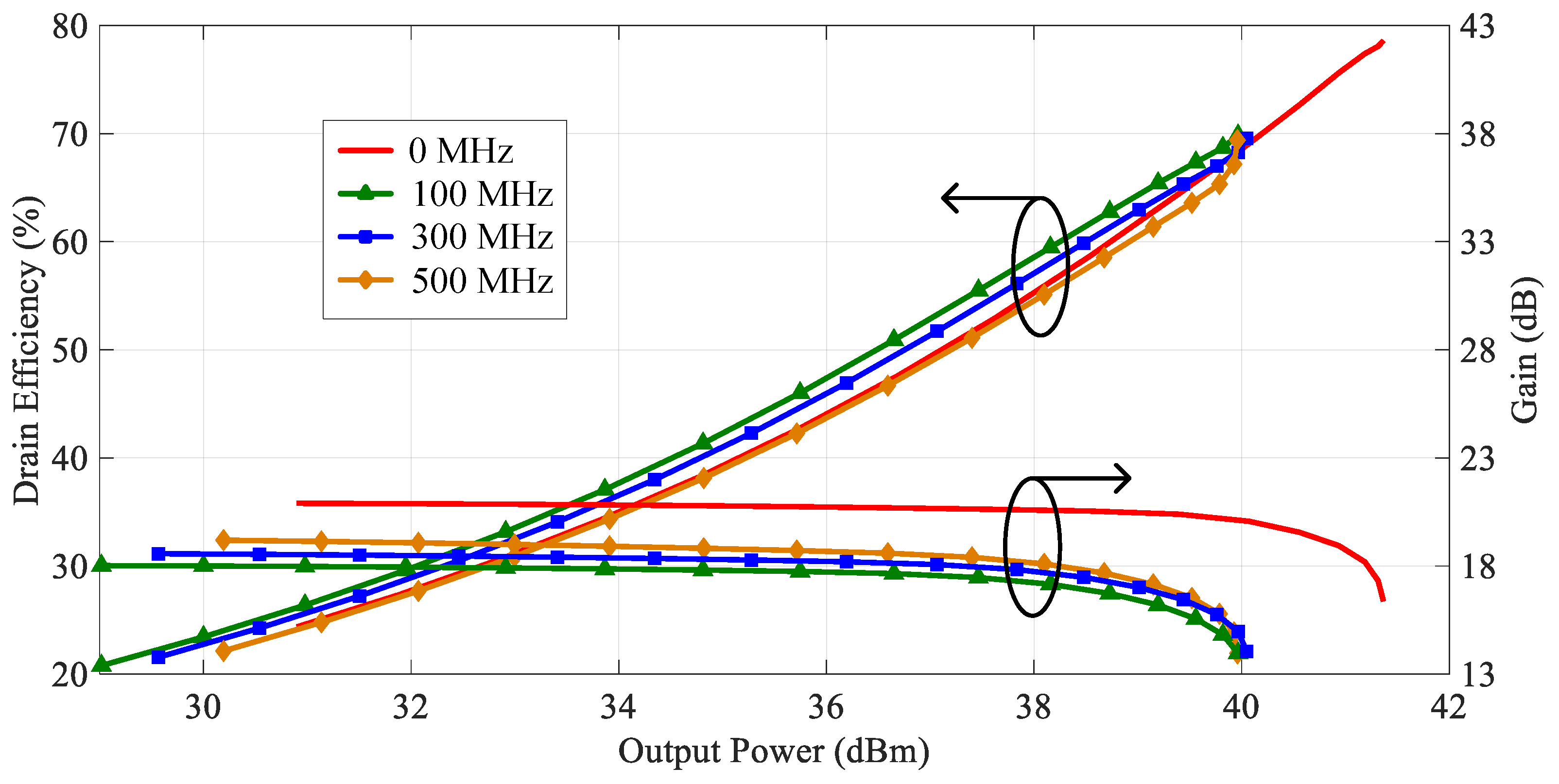
Secondly, to evaluate the performance of the fabricated PA, a two-tone CW signal, which is the same as in the simulation, is employed. The tone spacing of this concurrent two-tone CW signal is varied from 20 MHz up to 500 MHz. Figure 14 shows the measured concurrent DE and gain of the fabricated PA. The fabricated PA delivers a concurrent output power of 41.9 dBm when tone spacing is zero. Now, the measured DE and gain are 77.7% and 10.9 dB, respectively. Moreover, the measured concurrent output power remains above 39.6 dBm, and the measured concurrent DE exceeds 66.2% over a 500 MHz tone spacing.
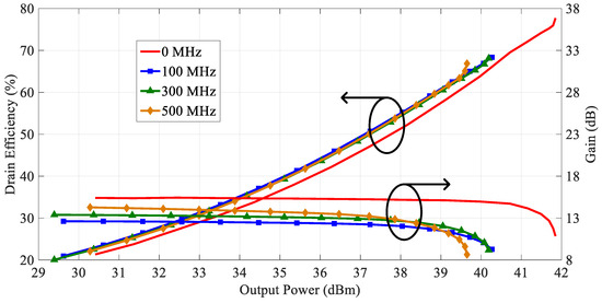
Figure 14.
Measured concurrent DE and gain versus output power of the fabricated PA under different tone spacing conditions.
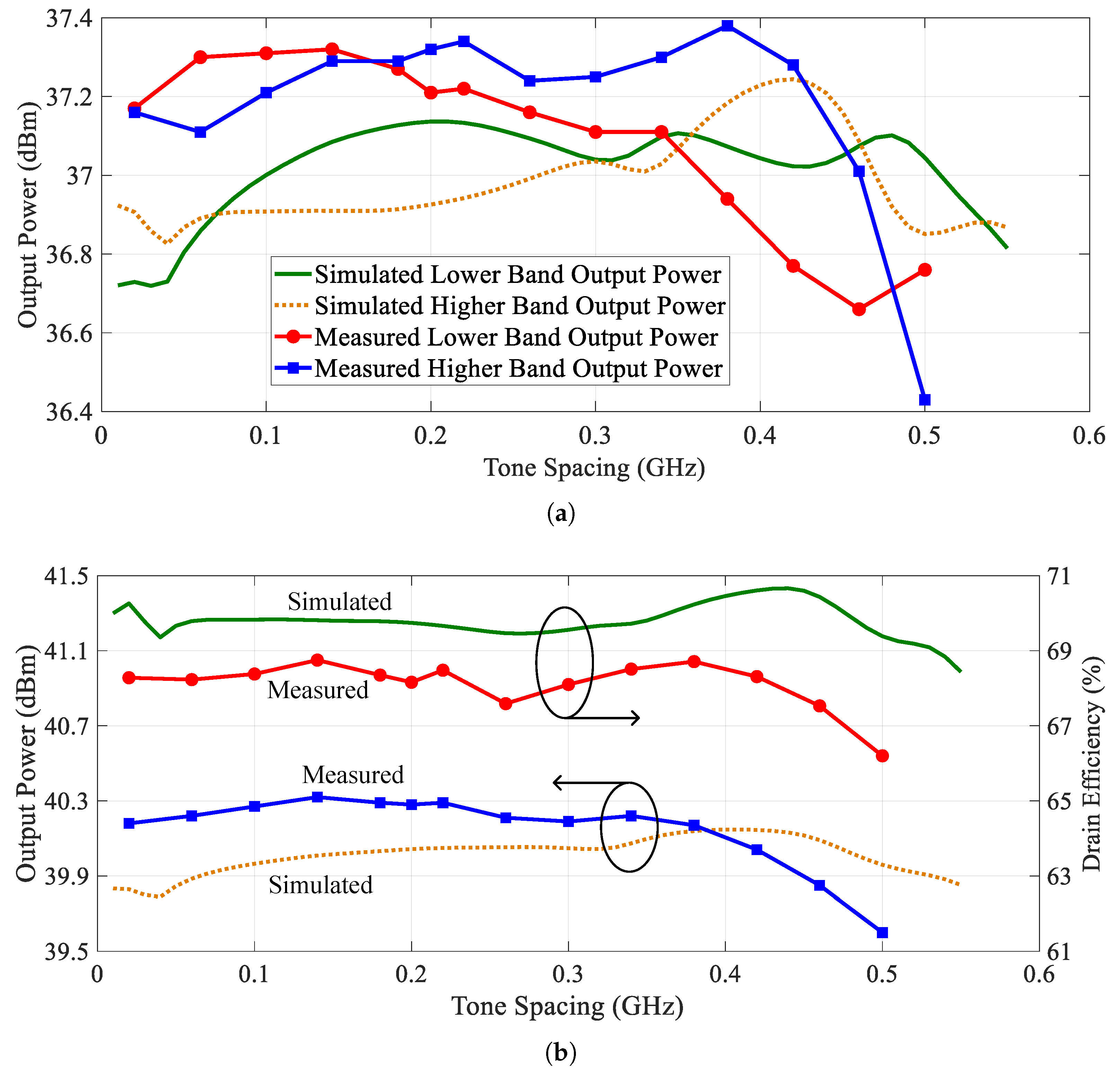
The measured concurrent performances of the fabricated PA at its saturation power level are presented in Figure 15a,b. From Figure 15a, the concurrent output power of the fabricated ranges from 36.7 dBm to 37.3 dBm in the lower frequency band and from 36.4 dBm to 37.4 dBm in the higher frequency band when the tone spacing is in the range of 20–500 MHz. Additionally, from Figure 15b, it can be observed that the fabricated PA achieves a concurrent DE of 66.2–68.8% and a concurrent output power of 39.6–40.3 dBm. For comparative purposes, Figure 15a,b illustrate the simulated concurrent output power and DE of the designed PA. It is noteworthy that due to the impact of non-ideal factors, such as processing and assembly errors, the test results exhibit a degradation compared to the simulation results, particularly when the tone spacing exceeds 450 MHz.
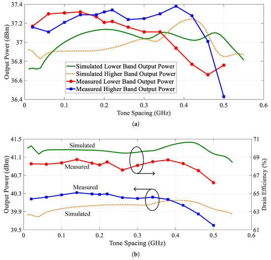
Figure 15.
(a) Measured concurrent output power of the fabricated PA versus tone spacing at lower and higher bands. (b) Measured concurrent DE and output power of the fabricated PA versus tone spacing at the saturation power level.
Table 1 lists the measurement results of the fabricated PA. For comparison, the measurement results of some state-of-the-art concurrent PAs are also given in Table 1. This work achieves a good performance under concurrent operation mode in terms of tone spacing and the concurrent efficiency, as shown in Table 1.

Table 1.
Measurement results of the state-of-the art concurrent PAs.
5. Conclusions
This paper presents a broadband PA which supports high-efficiency concurrent operation by controlling baseband impedance over a wide baseband frequency range. The performance of a concurrent dual-band PA is analyzed as a function of baseband impedance. It is indicated in this work that the imaginary part of the baseband impedance has a relatively minor effect on the concurrent performances compared to the real part. Consequently, when designing a broadband PA, we prefer the baseband impedance to vary along the edge of the Smith chart. In this work, we also propose a baseband impedance control method to design an 1.75–2.25 GHz PA. The fabricated PA achieves a maximum output power of more than 39.6 dBm with a DE of more than 66.2% over a tone spacing of 0–500 MHz.
Author Contributions
Writing—original draft preparation, X.M., F.L. and S.F.; writing—review and editing, X.L. (Xi Liu), X.L. (Xiaojiang Liu) and W.S.; supervision, W.S. All authors have read and agreed to the published version of the manuscript.
Funding
This research was funded by the Science and Technology Project of State Grid Sichuan Electric Power Company “Multi-dimensional Collaborative Anomaly-Awakening Sensor Network Technology for Transmission Lines in Complex Environments” (52199723000S).
Data Availability Statement
Data are contained within the article.
Conflicts of Interest
Authors Xiaomin Ma, Fan Liu, Songhai Fan, Xi Liu and Xiaojiang Liu was employed by the company State Grid Sichuan Electric Power Research Institute. The remaining authors declare that the research was conducted in the absence of any commercial or financial relationships that could be construed as a potential conflict of interest.
References
- Tao, M.; Chen, Y.; Kong, W.; Ni, S.; Zheng, Z.; Xia, J. Design of dual-mode multi-band Doherty power amplifier employing impedance-and-phase constrained optimization. Electronics 2025, 14, 2078. [Google Scholar] [CrossRef]
- Wei, Z.; Liu, H.; Yang, X.; Jiang, W.; Wu, H.; Li, X.; Feng, Z. Carrier aggregation enabled integrated sensing and communication signal design and processing. IEEE Trans. Veh. Technol. 2024, 73, 3580–3596. [Google Scholar] [CrossRef]
- Li, J.; Chen, W.; Huang, F.; Feng, Z. Multiband and multimode concurrent PA with novel intermodulation tuning network for linearity improvement. IEEE Microw. Wirel. Compon. Lett. 2018, 28, 248–250. [Google Scholar] [CrossRef]
- Saad, P.; Colantonio, P.; Piazzon, L.; Giannini, F.; Andersson, K.; Fager, C. Design of a concurrent dual-band 1.8–2.4-GHz GaN-HEMT Doherty power amplifier. IEEE Trans. Microw. Theory Tech. 2012, 60, 1840–1849. [Google Scholar] [CrossRef]
- Liu, W.; Liu, Q.; Du, G.; Li, G. Analytical dual-band matching approach for concurrent high-efficiency power amplifiers. IEEE Trans. Circuits Syst. II Express Briefs 2022, 69, 4769–4773. [Google Scholar] [CrossRef]
- Der, A.T.; Barton, T.W. C/Ka concurrent dual-band GaN MMIC based on shorted quarter-wavelength line topology. IEEE J. Microw. 2024, 4, 372–380. [Google Scholar] [CrossRef]
- Wei, L.; Chen, F.; Zhang, Z. Design of dual-band power amplifier based on microstrip coupled-line bandstop filter. AEU-Int. J. Electron. Commun. 2024, 183, 155381. [Google Scholar] [CrossRef]
- Cai, Q.; Che, W.; Ma, K.; Gu, L. A Concurrent dual-band high-efficiency power amplifier with a novel harmonic control network. IEEE Microw. Wirel. Compon. Lett. 2018, 28, 918–920. [Google Scholar] [CrossRef]
- Brinkhoff, J.; Parker, A.E. Effect of baseband impedance on FET intermodulation. IEEE Trans. Microw. Theory Tech. 2003, 51, 1045–1051. [Google Scholar] [CrossRef]
- Chen, X.; Chen, W.; Ghannouchi, F.M.; Feng, Z.; Liu, Y. Enhanced analysis and design method of concurrent dual-band power amplifiers with intermodulation impedance tuning. IEEE Trans. Microw. Theory Tech. 2013, 61, 4544–4558. [Google Scholar] [CrossRef]
- Shariatifar, M.; Jalali, M.; Abdipour, A. Design of a high-efficiency dual-band class-J/J power amplifier considering concurrent mode input drive. Int. J. RF Microw. Comput. Aided Eng. 2019, 30, e22064. [Google Scholar] [CrossRef]
- Bunz, B.; Ahmed, A.; Kompa, G. Influence of envelope impedance termination on RF behaviour of GaN HEMT power devices. In Proceedings of the European Gallium Arsenide and Other Semiconductor Application Symposium, GAAS 2005, Paris, France, 2–3 October 2005; pp. 649–652. [Google Scholar]
- Barros, D.R.; Nunes, L.C.; Cabral, P.M.; Pedro, J.C. Impact of the input baseband terminations on the efficiency of wideband power amplifiers under concurrent band operation. IEEE Trans. Microw. Theory Tech. 2019, 67, 5127–5138. [Google Scholar] [CrossRef]
- Nunes, L.C.; Barros, D.R.; Cabral, P.M.; Pedro, J.C. Efficiency degradation analysis in wideband power amplifiers. IEEE Trans. Microw. Theory Tech. 2018, 66, 5640–5651. [Google Scholar] [CrossRef]
- Qi, T.; He, S.; Hu, B.; Liu, C.; Du, X.; Zhao, Y.; Helaoui, M.; Chen, W.; Ghannouchi, F.M. Efficiency analysis of concurrently driven power amplifiers. IEEE Access 2020, 8, 91379–91393. [Google Scholar] [CrossRef]
- Huang, H.; Yu, C.; Wu, Y.; Jin, Q.; Fan, C.; Gao, J.; Liu, Y. Analysis and design of a novel concurrent class B/J continuum power amplifier. Int. J. RF Microw. Comput. Aided Eng. 2020, 30, e22275. [Google Scholar] [CrossRef]
- Shariatifar, M.; Jalali, M.; Abdipour, A. A concurrent dual-band continuous Class-F power amplifier with intermodulation impedance tuning: Analysis and design technique. AEU-Int. J. Electron. Commun. 2019, 111, 152899. [Google Scholar] [CrossRef]
- Liu, J.; Shi, W.; Zang, Y.; Hua, J.; Xu, G.; Hu, C.; Liu, K.; Li, Y.; Li, M. Analysis and design of concurrent class-F2 power amplifier based on power-series technique. AEU-Int. J. Electron. Commun. 2025, 193, 155722. [Google Scholar] [CrossRef]
- Yao, Y.; Dai, Z.; Li, M. A novel topology with controllable wideband baseband impedance for power amplifiers. Front. Inf. Technol. Electron. Eng. 2024, 25, 308–315. [Google Scholar] [CrossRef]
- Liu, K.; Shi, W.; Lu, N.; Li, Y.; Liu, J.; Zang, Y.; Hu, C.; Li, M. Broadband Doherty power amplifier with baseband impedance control for concurrent application. AEU-Int. J. Electron. Commun. 2025, 191, 155680. [Google Scholar] [CrossRef]
Disclaimer/Publisher’s Note: The statements, opinions and data contained in all publications are solely those of the individual author(s) and contributor(s) and not of MDPI and/or the editor(s). MDPI and/or the editor(s) disclaim responsibility for any injury to people or property resulting from any ideas, methods, instructions or products referred to in the content. |
© 2025 by the authors. Licensee MDPI, Basel, Switzerland. This article is an open access article distributed under the terms and conditions of the Creative Commons Attribution (CC BY) license (https://creativecommons.org/licenses/by/4.0/).


