Article

Highly Robust Active Damping Approach for Grid-Connected Current Feedback Using Phase-Lead Compensation

School of Electrical Engineering, Xinjiang University, Urumqi 830017, China
*
Author to whom correspondence should be addressed.
Electronics 2025, 14(2), 309; https://doi.org/10.3390/electronics14020309
Submission received: 12 December 2024 / Revised: 11 January 2025 / Accepted: 13 January 2025 / Published: 14 January 2025

Abstract

:
The grid-current-feedback active damping (GCFAD) strategy has been widely utilized in LCL-type cascaded H-bridge static var generator (SVG) systems. Although digital control in GCFAD enhances sampling accuracy, it introduces delays in the subsequent calculation and execution processes, thereby reducing the effective damping region and weakening the robustness of the LCL-type cascaded H-bridge SVG system under a broad domain of grid impedance changes. This paper expands the effective damping area from (0, fR) (fR ∈ (fs/6, fs/3)) to (0, 0.45fs) by introducing a phase-lead compensator into the active damping feedback loop to reduce the delay. This reduces the negative effect of the digital control on the system’s effective damping region and significantly enhances its robustness under an extensive domain of grid impedance variations. The improved GCFAD is employed to establish the system’s discrete domain model and the controller parameters are adjusted in conjunction with the mentioned model. Simulation outcomes indicate the efficiency of the presented approach.

Graphical Abstract

1. Introduction

The integration of nonlinear loads has exacerbated issues such as low power factor, harmonic pollution, and three-phase imbalances in the power grid, leading to a significant decline in power quality. The LCL-type cascaded H-bridge static var generator (SVG), a novel compensation device, is widely used in power systems for reactive power compensation, owing to its superior dynamic adjustment and harmonic suppression capabilities [1]. However, connecting the cascaded H-bridge SVG to the grid may induce high-frequency resonance due to its interaction with the LCL filter. Additionally, large variations in grid impedance can shift resonance frequencies, impairing system stability and distorting the output current [2,3,4]. In weak grid environments, such as those with high-penetration renewable energy or long-distance transmission systems characterized by low short-circuit ratios (SCR) or high impedance ratios (ZR), this resonance issue is particularly severe and poses a potential threat to the safe operation of power systems.
Traditional methods used to address the resonant problem of LCL filters involve passive and active damping. Passive damping [5,6,7,8], which suppresses resonance by introducing actual resistance, shows significant results, but increases power consumption and hardware costs. Active damping [9,10,11,12,13,14,15], especially the grid-current-feedback active damping (GCFAD) approach based on virtual resistance, has gradually become mainstream owing to its flexibility and lack of extra power consumption [16,17,18,19,20]. However, control delay narrows the effective damping region, leading to poor performance of the system in complex grid environments, where it struggles to cope with grid impedance variations. Studies on active damping strategies [9,10,11,12,13,14,15] indicate that the virtual resistance method simulates the damping effect of actual resistance by feeding back the appropriate state variables. While its flexibility enhances system stability, control delay remains an issue in digital systems. Control delay shrinks the effective damping region [18], making the system prone to instability under significant variations in the grid impedance.
Various studies have attempted to improve the GCFAD strategy to address the issue of control delay. A study [21] analyzed the impact of delay on virtual impedance and proposed an active damping critical value model, revealing the intrinsic relationship between control delay and system stability. However, it did not fully bring up the effect of grid impedance variations on the system’s resonant frequency, restricting its applicability when grid impedance undergoes significant variations. Some methods, like real-time sampling and multi-sampling techniques, have been proposed to reduce control delay by directly modifying the sampling method [22,23,24]. However, delays cannot be entirely eliminated due to computational speed limitations, and there is a risk of introducing aliasing and switching noise, which can affect system stability. Other studies [19,20] introduced a delay compensation loop within the active damping loop to extend the effective damping region, thus improving system stability. However, existing compensators have limited capacity, and the effective damping region extension is restricted. Besides, the system lacks robustness and adaptability, particularly in weak grid environments. Overall, since existing research has not effectively expanded the damping region of the system, stable operation cannot be ensured under significant variations in grid impedance. Further optimization is required to improve system robustness and adaptability.
To address the above problems, the current study presents a highly robust GCFAD approach using phase-lead compensation. Section 2 configures and models a typical cascaded H-bridge SVG system containing LCL filtering links and presents the system control structure using the conventional GCFAD strategy. Section 3 analyzes the adverse effect of digital control delay on the conventional GCFAD. Section 4 introduces a phase-lead compensator, whose optimal coefficient is derived, which is chosen as 0.95. The compensated GCFAD parameters are then redesigned and analyzed to guarantee the system’s stability. The compensator significantly expands the GCFAD system’s effective damping area from (0, fR) (fR ∈ (fs/6, fs/3)) to (0, 0.45fs), thereby improving the system’s stability and robustness under a broad domain of grid impedance changes. Section 5 provides the simulation and comparative analysis outcomes to evaluate the capability of the improved robust GCFAD strategy to effectively suppress resonance and enhance the quality of grid-connected (GC) current.

2. Modeling of the LCL-Type Cascaded H-Bridge SVG System

2.1. Main Circuit Topology

Figure 1 presents the structure diagram of the cascaded H-bridge SVG system. The main circuit adopts a star structure, where H-bridge modules are cascaded to form three phases linked to the grid via an LCL-type filter. In Figure 1, upcck(k = a, b, c) describes the grid connection point voltage; usk(k = a, b, c) describes the grid voltage; Lgk(k = a, b, c) describes the grid inductance; the SVG side inductance L1, the filter capacitor C, and the grid-side inductance L2 form the LCL-type filter; i1k(k = a, b, c) and i2k(k = a, b, c) describe the currents of L1 and L2, respectively; uck(k = a, b, c) describes the filter capacitor voltage; udc represents the equivalent single H-bridge DC voltage of the three-phase DC side; Cdc represents the equivalent capacitance.
To more efficiently analyze the digital control delay, the following assumptions are made for system simplification. All power switches are assumed to be ideal switches, ignoring the effects of switching dead time. The inductors and capacitors in the filter are considered ideal components, excluding parasitic resistance. The grid voltage is assumed to be a perfectly symmetrical three-phase ideal sinusoidal wave.

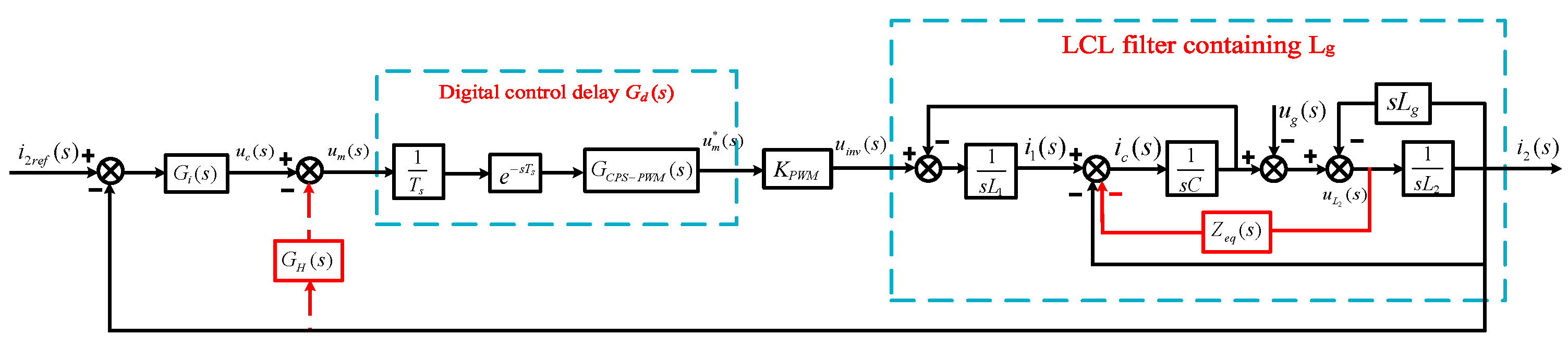
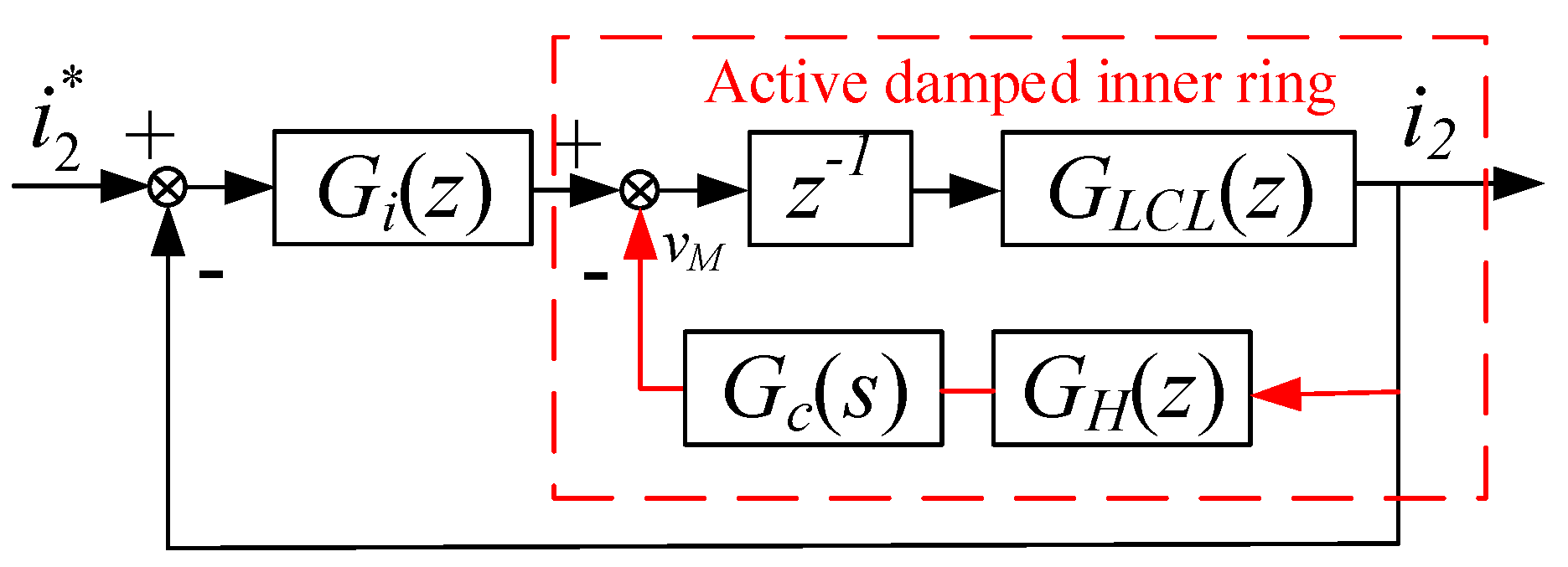
2.2. System Control Framework

The control framework of the LCL-type cascaded H-bridge SVG is typically divided into an inner current loop and an outer voltage loop. The current study mainly focuses on the inner current loop while neglecting the impact of the outer voltage one. A pulse width modulation (PWM) CPS-PWM is employed in a two-phase stationary coordinate system, with a sampling rate fs equal to the switching rate fsw. The current loop employs a proportional–integral (PI) controller. Figure 2 describes the traditional GCFAD system’s equivalent control block diagram in the continuous domain.
In Figure 2, Gi(s) is the current controller; KPWM indicates the H-bridge SVG’s equivalent gain; Gd(s) describes the digital control system’s equivalent delay element; and GH(s) is the high-pass filter (HPF). The current controller Gi(s) is a PI regulator whose transfer function (TF) is given by:
G i ( s ) = K p + K i s
Kp represents the proportional coefficient; Ki represents the resonance coefficient.
Gd(s) denotes the system control delay formed by the sampling process, computational delay, and zero-order hold, described as follows:
G d ( s ) = 1 T s e s T s T s e 0.5 s T s = e 1.5 s T s
The active damping function GH(s) comprises a first-order HPF and a transfer function. Its expression is:
G H ( s ) = s K H s + ω d
where KH describes the damping coefficient and ωd indicates the cutoff angular frequency.
From Figure 2, the LCL filter’s equivalent TF from uinv(s) to i2(s), denoted by GLCL(s), can be expressed as:
G L C L ( s ) = i 2 ( s ) u i n v ( s ) = 1 s 3 L 1 ( L 2 + L g ) C + s ( L 1 + L 2 + L g ) = 1 s L 1 ( L 2 + L g ) C 1 s 2 + ω r 2
where ωr indicates the LCL filter’s resonant angular frequency, calculated as follows:
ω r = L 1 + L 2 + L g C L 1 ( L 2 + L g )

3. Impact of Digital Control Delay on Traditional GCFAD

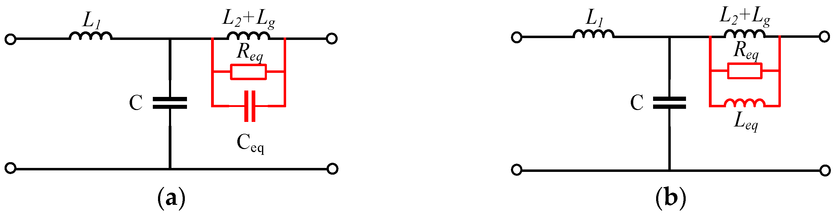
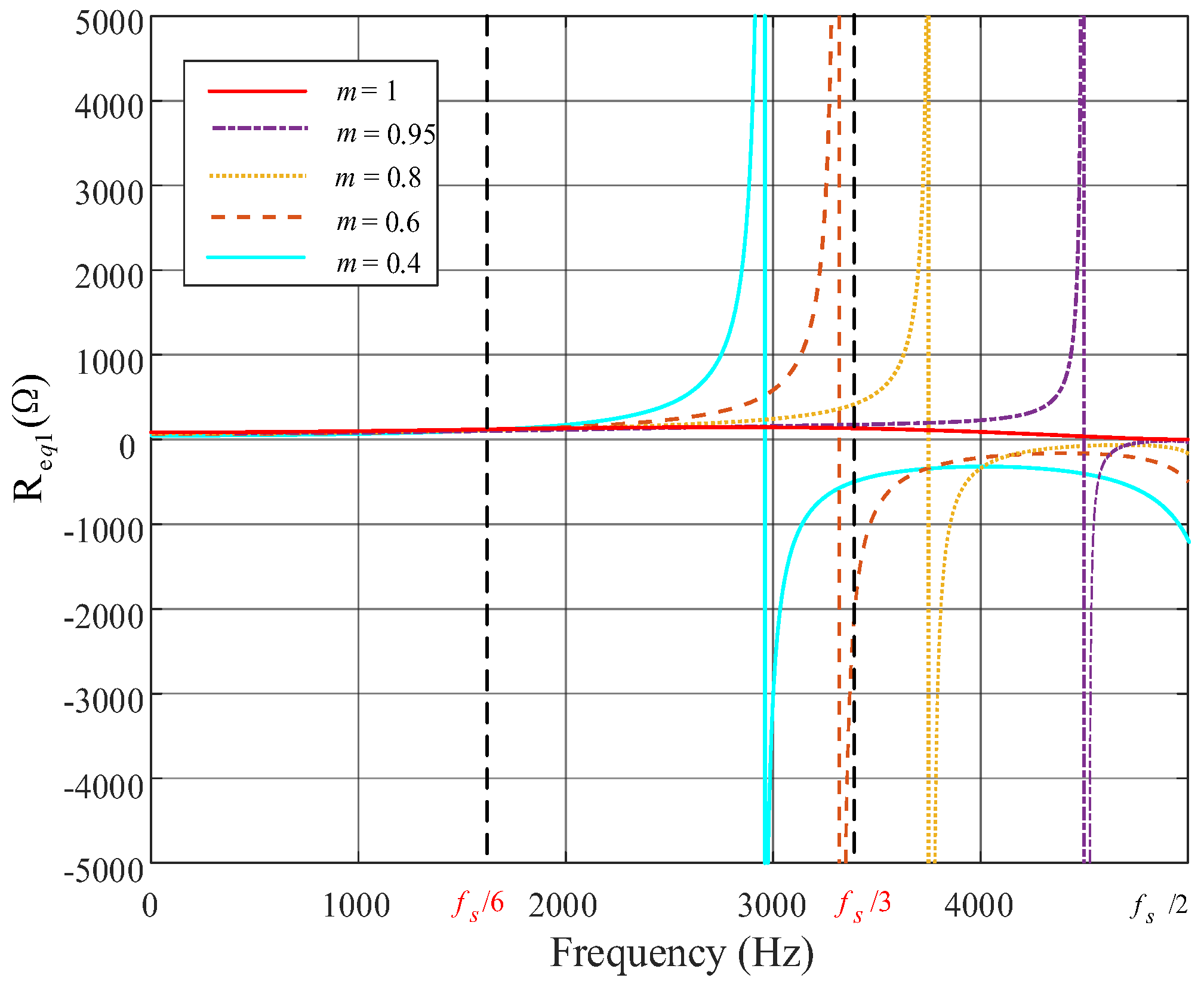
3.1. Virtual Impedance Analysis Under Digital Control

Figure 2 can be transformed accordingly to obtain the equivalent virtual impedance of the GCFAD strategy and analyze its physical essence. Specifically, the starting point of the active damping function GH(s) is adjusted from the GC current i2(s) to the grid-side inductive voltage uL2(s), and its endpoint is changed to the output terminal of the cascaded H-bridge SVG-side inductive current i1(s). This forms the equivalent control block diagram presented in Figure 3, reflecting the active damping strategy’s physical nature. This strategy essentially connects a virtual impedance Zeq(s) in parallel across the two terminals of the grid-side inductance L2, which can be expressed as:
Z e q ( s ) = s ( s + ω d ) L 1 ( L 2 + L g ) e 1.5 s T S K P W M K H
When Gd(s) = 1, the virtual impedance Zeq(s) is unaffected by digital control delays. In this case, the grid-current-feedback active damping strategy is equivalent to parallel connecting a virtual impedance, which remains positive in the frequency range (0, fs/2), across both ends of L2. This configuration helps dampen the resonance peaks across all resonant frequency ranges of the LCL filter. However, digital control delays narrow the effective damping range of the GCFAD method, limiting it to (0, fR), where fR ∈ (fs/6, fs/3).
After introducing virtual impedance, the resonant characteristics of the LCL filter will be improved. In the positive resistance region, Zeq(s) can effectively dampen the system’s resonance peaks, reducing their amplitude and, thus, suppressing system instability.
By inserting s = jω into (6), the frequency-domain representation of Zeq is obtained as:
Z e q ( j ω ) = ω L 1 ( L 2 + L g ) ( ω j ω d ) K P W M K H [ cos ( 1.5 ω T s ) + j sin ( 1.5 ω T s ) ]
Equation (7) describes a parallel combination of a resistance Req(ω) and a reactance Xeq(ω), expressed as follows:
Z eq ( j ω ) = R eq ( ω ) / / X eq ( ω )
Req(ω) and Xeq(ω) are calculated as:
R eq ( ω ) = ω L 1 ( L 2 + L g ) ( ω 2 + ω d 2 ) K P W M K H M ( ω ) X eq ( ω ) = ω L 1 ( L 2 + L g ) ( ω 2 + ω d 2 ) K P W M K H N ( ω )
where
M ( ω ) = ω cos ( 1.5 ω T s ) + ω d sin ( 1.5 ω T s ) N ( ω ) = ω sin ( 1.5 ω T s ) ω d cos ( 1.5 ω T s )
The frequency features of Req and Xeq can be obtained from Equation (9). When Req exhibits positive resistance features, it effectively suppresses the LCL filter’s resonance, as presented in Figure 4. Req exhibits positive resistance behavior within the frequency range (0, fR), which corresponds to the system’s valid damping range, and negative resistance behavior within (fR, fs/2), where fR ∈ (fs/6, fs/3). In the most severe case, the frequency boundary fR of the positive and negative resistances of Req is fs/6. When the system’s resonant frequency fr is greater than fs/6, i.e., fr > fR, the negative resistance characteristic of Req will degrade the system’s robustness to grid impedance, particularly when fr = fR, where the system cannot maintain stability.
From the analysis above, it can be concluded that using the GCFAD method not only virtualizes resistance, but also introduces an equivalent inductance or capacitance, and the equivalent reactance Xeq (either capacitive or inductive) causes a shift in fr. Figure 5 presents the equivalent virtual impedance circuit.
From Figure 5, the resonant frequency of the system’s loop gain is obtained as:
f r = 1 2 π L 1 + L 2 + L g ( C + C e q ) L 1 ( L 2 + L g ) , X e q = C e q 1 2 π L 1 + L 2 + L g C L 1 ( L 2 + L g ) + 1 C L e q , X e q = L e q

3.2. Stability Verification of the Traditional GCFAD System

From Figure 3, the transfer function of the loop gain of the digital-controlled LCL-type GC cascaded H-bridge SVG, denoted by TD(s), can be expressed as:
T D ( s ) = 1 s 3 L 1 L 2 C G i ( s ) K P W M e 1.5 s T s s 2 + ω r 2 + s C Z e q ( s )
As shown in (12), the numerator of TD(s) includes the control delay term e−1.5sTs, which causes phase lag and limits the control loop’s bandwidth; the equivalent impedance Zeq of the actively damped loop in the denominator restricts the control loop’s bandwidth, which influences the system’s dynamic efficiency.
Figure 6 shows the loop gain’s Bode diagram under various grid impedances for the digital-controlled cascaded H-bridge SVG based on Equation (12) and the system parameters in Table 1.
As illustrated in Figure 6, the wide range of grid impedance Lg changes causes the resonant peak frequency to cross the positive and negative dividing frequency fR of the virtual resistor Req. Combined with Figure 4, it is known that, when fr > fR, the virtual resistor Req exhibits a negative resistance characteristic. In this case, the active damping controller amplifies the resonant frequency signal instead of suppressing it, ultimately leading to system instability. Furthermore, Equations (5) and (11) show that the loop gain’s resonant frequency fr is greater than fr, indicating that Req < 0 at fr. For the traditional GCFAD method, the phase frequency response of the open-loop TF TD(s) never crosses −180°. In addition, TD(s) has poles in the right half-plane (RHP) when fr > fR. Therefore, from the Nyquist stability criterion, the system is unable to operate stably when fr’ > fR.
To improve the system’s stability and robustness, the delay should be reduced to increase the system’s boundary frequency, ensuring fR > fr’. This will avoid negative resistance in the frequency range lower than fr’. If fR = fs/2, Req has a positive resistance within the Nyquist frequency, significantly improving system performance.

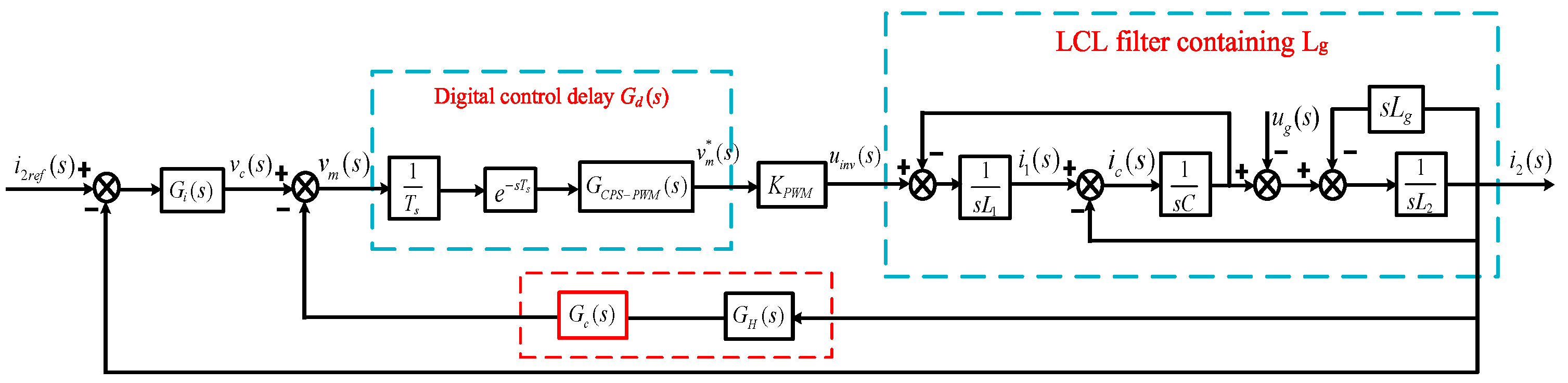
4. Highly Robust GCFAD Strategy Based on Phase-Lead Compensator

The analysis in Section 3 indicates that the valid damping zone of the traditional GCFAD system is confined to the range (0, fR), where fR lies within the range of (fs/6, fs/3). Since the grid impedance variations can cause shifts in the system’s resonant frequency, the narrow valid damping zone may lead to the virtual resistance falling into the negative resistance region. Therefore, the traditional damping approach should be refined to enlarge the efficient damping area and improve the system’s robustness. The current work introduces a phase-lead compensator in the damping loop to counteract the negative effects of digital delay on the effective damping region, as presented in Figure 7.
The TF of the delay compensation link, denoted by Gc(s), is represented as:
G c ( s ) = ( 1 + m 1 + m e s T s ) 2
where 0 ≤ m ≤ 1 and where m represents the degree of compensation. When m = 0, no compensation is applied, and, when m = 1, full compensation is applied. Within the Nyquist frequency range (0, fs/2), replacing e s T s with z in (13) gives:
G c ( z ) = ( 1 + m 1 + m z 1 ) 2
According to Equation (14), the delay compensator’s frequency response characteristics can be changed by adjusting the value of m, as depicted in Figure 8.
As presented in Figure 8, the phase provided by the compensator increases as the value of m increases. When m = 1, the phase at the Nyquist frequency is 180°, while the corresponding excessive amplitude gain amplifies high-frequency noise, resulting in system instability. Therefore, a trade-off must be made between the phase and the amplitude of the compensation link to attain a satisfactory compromise between phase compensation while considering the stability of the system, and m ∈ (0.8, 1) was selected after the analysis.

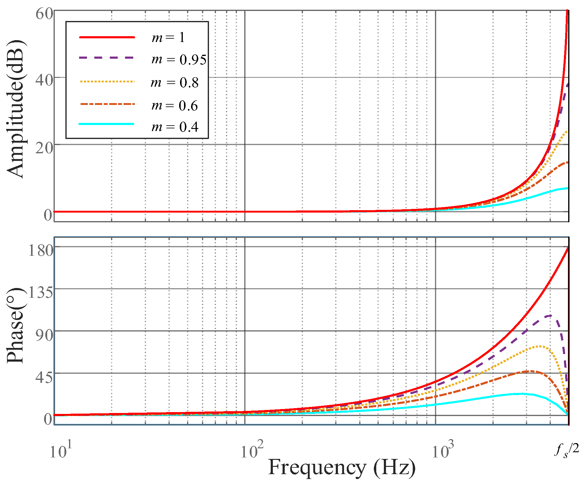
4.1. Effective Damping Zone Analysis

After adding the phase-lead compensation link, the virtual equivalent impedance Zeq1 connected in parallel at both ends of L2 can be expressed as:
Z e q 1 ( s ) = s ( s + ω d ) L 1 ( L 2 + L g ) e 1.5 s T S ( 1 + m e s T s ) 2 K P W M K H ( 1 + m ) 2
Substituting s = into (15) gives the frequency-domain representation for Zeq1 as:
Z e q 1 ( j ω ) = L 1 ( L 2 + L g ) K P W M K H ( 1 + m ) 2 ( M 1 + j N 1 )
M 1 = ω 2 [ cos 3 π f T s + ( m 2 + 2 m ) cos π f T s ] + ω ω d [ sin 3 π f T s + ( 2 m m 2 ) sin π f T s ] N 1 = ω 2 [ sin 3 π f T s + ( 2 m m 2 ) sin π f T s ] ω ω d [ cos 3 π f T s + ( m 2 + 2 m ) cos π f T s ]
This can be equivalently represented by a resistance Req1(ω) in parallel with a reactance Xeq1(ω):
Z eq 1 ( j ω ) = R eq 1 ( ω ) / / X eq 1 ( ω )
where the frequency-domain representations of Req1(ω) and Xeq1(ω) are:
R eq 1 ( ω ) = L 1 ( L 2 + L g ) K P W M K H ( 1 + m ) 2 M 1 2 + N 1 2 M 1 X eq 1 ( ω ) = L 1 ( L 2 + L g ) K P W M K H ( 1 + m ) 2 M 1 2 + N 1 2 N 1
Combining Equations (17) and (19), the frequency characteristics of Req1 and Xeq1 for different values of m are illustrated in Figure 9.
As presented in Figure 9, the positive and negative dividing frequencies of the equivalent damping resistance Req1 are improved after introducing the delay compensation link, and the system’s effective damping area is effectively enlarged with the increase of m. To determine the optimal value of the compensation coefficient m, the closed-loop poles (CLPs) are obtained by changing the compensation coefficient m using the parameters given in Table 1, as presented in Figure 10.
It can be observed that, as m increases, the CLPs progressively shift outside the unit circle. To ensure the system stability when the system’s actual resonant frequency traverses the dividing frequency under a weak grid, the maximum value of m was chosen as 0.95 to attain a wide positive damping range (0, 0.45fs), and the system’s effective damping region covered almost all possible resonant frequencies. Therefore, extending the effective damping region by phase-lead compensation significantly improves the system’s stability, especially under complex grid situations, improving the system’s adaptability and robustness.

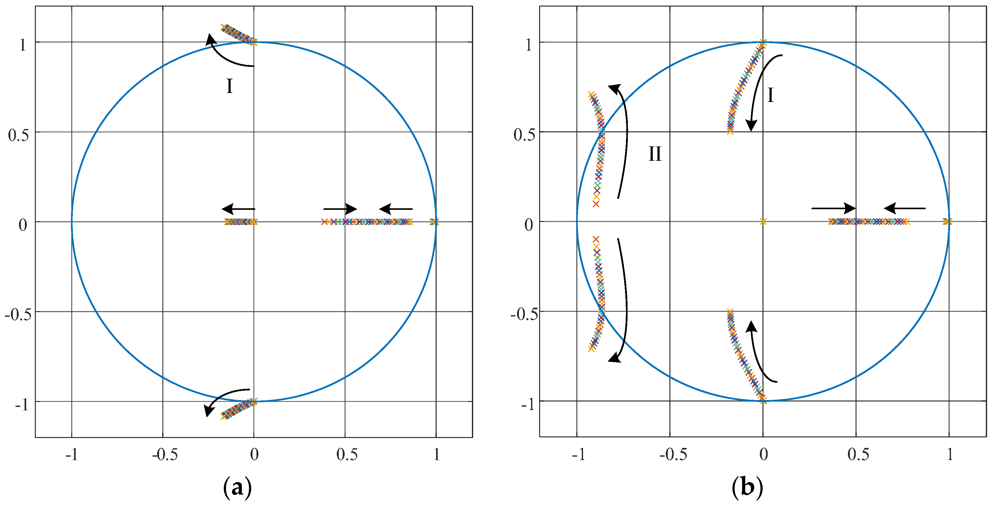
4.2. Design and Stability Analysis of GC Current Feedback Coefficient KH

The magnitude of the GC current feedback coefficient affects the number of RHP poles and the magnitude margin of the system’s loop gain. The pole distribution of the loop gain of the LCL-type cascaded H-bridge SVG system should be analyzed after the compensation. Due to the existence of nonlinear links in the open-loop gain derived from the s-domain control block diagram, the continuous links in the control system shown in Figure 2 should be discretized for ease of analysis, forming the system control’s z-domain block diagram presented in Figure 11.
Where GLCL(z) is the z-domain transfer function discretized by the series connection of the zero-order keeper link and the main circuit of the cascaded H-bridge SVG, which is expressed as:
G L C L ( z ) = K P W M ω r ( L 1 + L 2 + L g ) [ ω r T s z 1 ( z 1 ) sin ( ω r T s ) z 2 2 z cos ( ω r T s ) + 1 ]
GH(z) indicates the discrete TF of the active damped feedback function GH(s) discretized using the bilinear method, which can solve the frequency-domain aliasing distortion problem caused by time-domain sampling, and its expression is:
G H ( z ) = Z [ s K H s + ω d ] s = 2 T s z 1 z + 1 = 2 K H ( z 1 ) ( 2 + ω d T s ) z + ( ω d T s 2 )
For the high-frequency case, the GPI(s) is equivalent to a Kp link. The z-domain open-loop TF, using the improved GCFAD system, can be attained.
T D ( z ) = { K p A { ω r T s [ z 2 2 z cos ( ω r T s ) + 1 ] ( z 1 ) 2 sin ( ω r T s ) } [ ( 2 + ω d T s ) z + ( ω d T s 2 ) ] ( z + m ) 2 } { ( z 1 ) { z [ z 2 2 z cos ( ω r T s ) + 1 ] [ ( 2 + ω d T s ) z + ( ω d T s 2 ) ] ( z + m ) 2 2 A K H ( 1 + m ) 2 { ω r T s [ z 2 2 z cos ( ω r T s ) + 1 ] ( z 1 ) 2 sin ( ω r T s ) } } }
where
A = K P W M ω r ( L 1 + L 2 + L g )
After selecting the compensation coefficient to be m = 0.95, the system’s closed-loop polar plot for various values of the grid-connected current feedback coefficient KH (KH ∈ (0, 1)) was plotted, as presented in Figure 12:
Figure 12a illustrates the pole distribution of the closed-loop TF of the system prior to time-delay compensation. As depicted in Figure 12a, In region Ⅰ, the CLPs moves outside the unit circle as the value of KH increases. In contrast, for small values of KH, the pole, although still within the unit circle, is positioned near its boundary, resulting in a limited stability margin and suboptimal damping performance for the uncompensated system.
Figure 12b illustrates the CLP distribution of the compensated system. In region Ⅰ, for the same value of KH, the CLPs of the compensated system are positioned closer to the inner unit circle, resulting in an improved stability margin. This demonstrates that the presented delay compensation approach efficiently enhances the stability of the GC current under weak grid conditions and strengthens the system’s robustness. In region Ⅱ, as KH increases, the CLPs of the system move away from the circle. According to automatic control theory, poles closer to the origin provide better damping performance. To address the impact of system parameter changes on pole position, a comprehensive analysis was conducted to determine an optimal KH value. In this study, KH = 0.5 was chosen to fulfill the system’s stability requirements.
Since the cutoff frequency ωd is positively correlated with KH, it is necessary to obtain the range of ωd constraints that provides an open-loop gain with no RHP poles. Based on the selected values of m and KH, the closed-loop system’s polar plot for different values of ωd (ωd ∈ (0, ωr)) is shown in Figure 13.
As described in Figure 13, with the gradual growth of ωd, the CLPs in the I-area will gradually approach the unit circle, ωd = 0.6. A ωr ≈ 9425 was taken to locate the poles of the open-loop gain in the left half-plane (LHP) while obtaining a satisfactory stability amplitude margin.

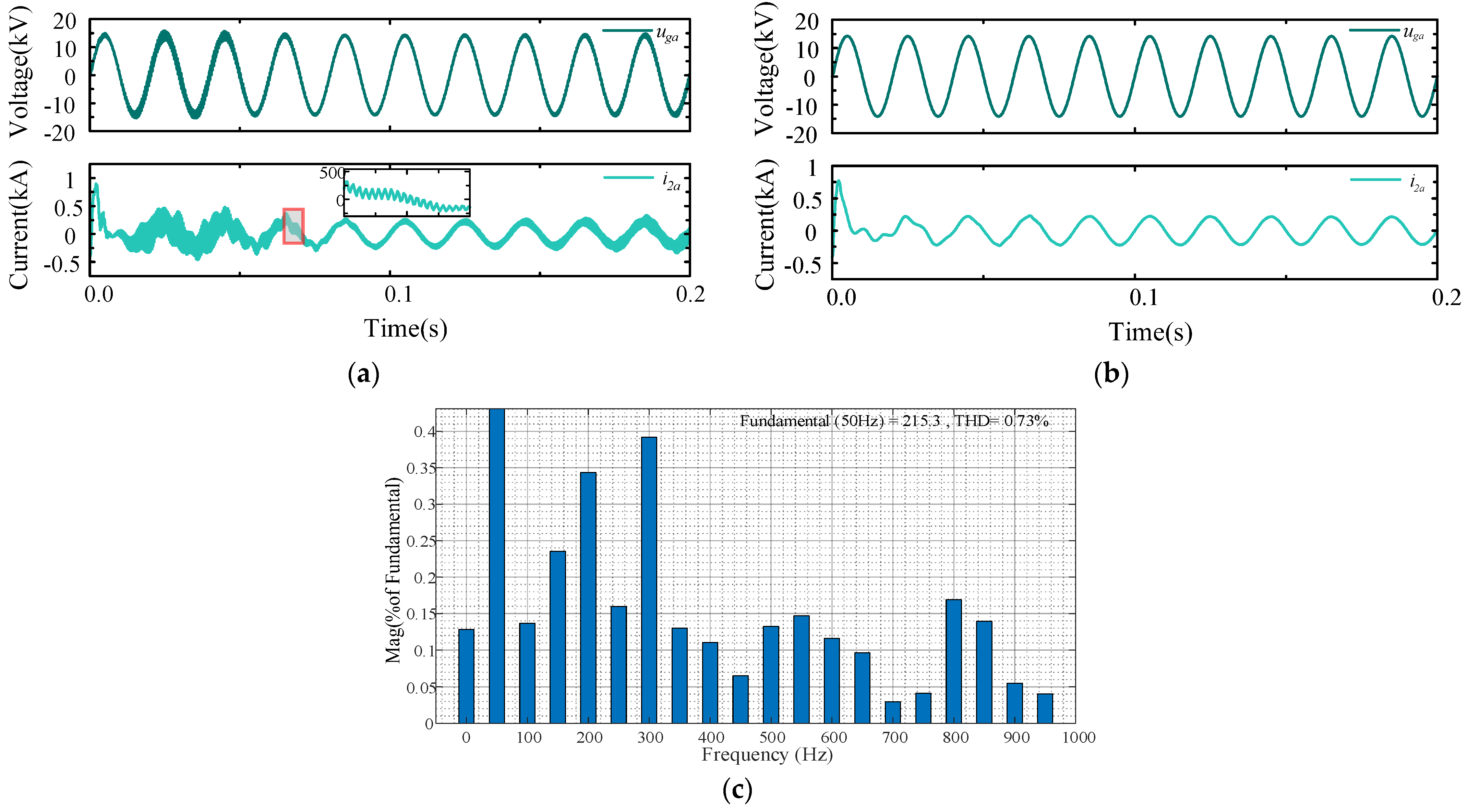
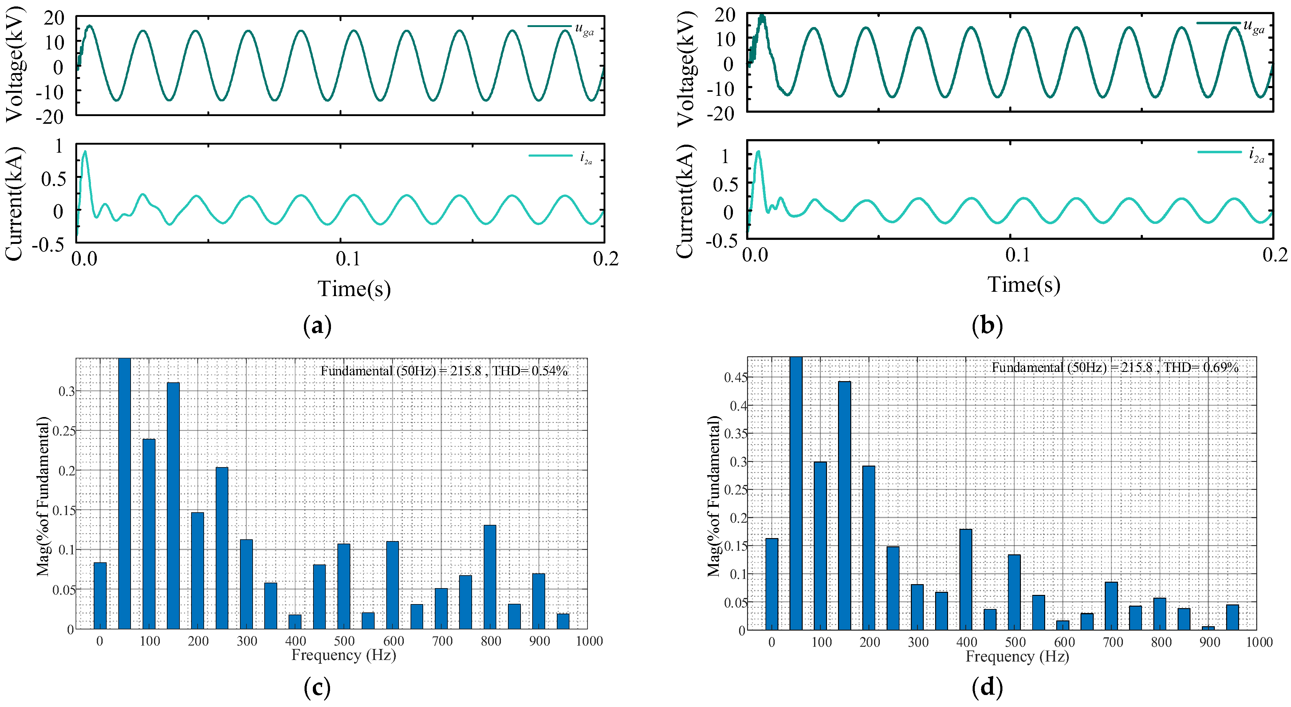
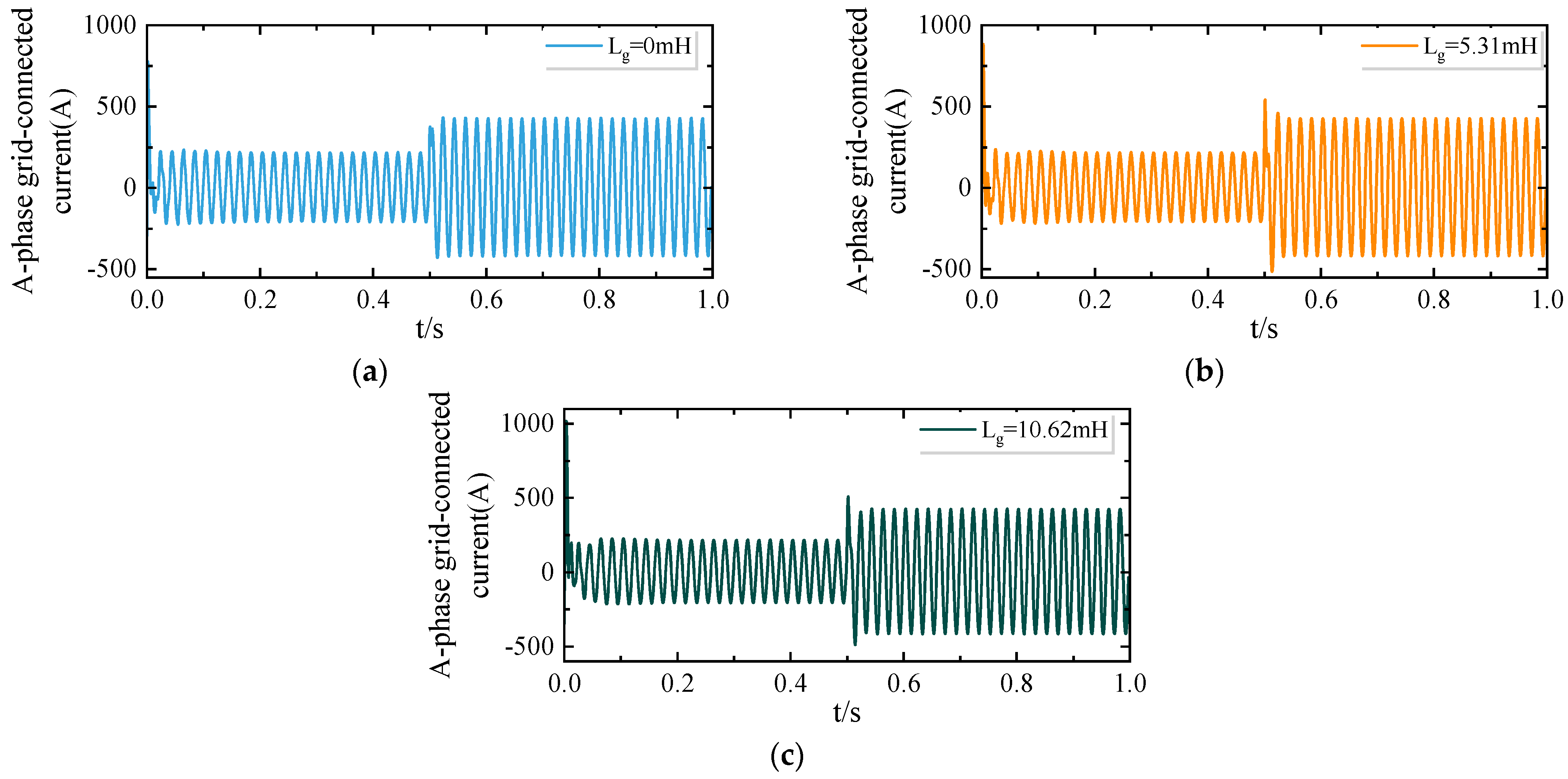
5. Simulation and Verification

To assess the accuracy and feasibility of the presented approach, a highly robust GCFAD system simulation model was developed by MATLAB R2022b/Simulink. Table 1 presents the system’s main circuit parameters.
Figure 14 presents the A-phase grid-connected voltage and grid-connected current of the GCFAD system before and after compensation for Lg = 0 and fr = 2.49 kHz. As shown in Figure 14a, the resonance occurred with the conventional GCFAD system, causing a risk of instability. Figure 14b presents the system’s A-phase GC voltage and current using highly robust GCFAD. A comparison with Figure 14a shows that the compensated system can effectively suppress system resonance at the resonant frequency. As presented in Figure 14c, the THD of the system with highly robust GCFAD was only 0.77%, satisfying the grid-connection requirements.
Figure 15 describes the system’s simulated waveforms after the compensation for various values of the grid impedance. Combined with the case of Figure 14b, the system was kept stable when the grid impedance changed within 0–10.62 mH, demonstrating that the proposed highly robust GCFAD strategy can provide better stability and robustness under a broad domain of grid impedance changes.
Figure 16 illustrates the dynamic waveform of the load surge current for different values of the grid impedance. At t = 0.5 s, the load changed from 4 Mvar inductive load to 4 Mvar capacitive load.
As presented in Figure 16, the grid-connected current was rapidly regulated and provided stable operation after two IF cycles after a sudden load change. This delivered an effective damping effect while also reflecting the system’s rapid dynamic response.
The above simulation results indicate that the proposed highly robust GCFAD strategy can provide a satisfactory damping effect and a wide damping region, thereby improving the system’s adaptability to the weak grid. This demonstrates the effectiveness of the highly robust GCFAD method in suppressing harmonics and improving system stability and power quality.

6. Conclusions

This paper investigates the stability and harmonic suppression of the GCFAD control system to solve the insufficient robustness and poor harmonic suppression of conventional control strategies under complex grid conditions. The current study shows that the traditional GCFAD control strategy has limited harmonic suppression capability and poor system stability and robustness under complex grid conditions due to the delay effect. For this reason, the current study introduces a highly robust GCFAD control approach using phase overrun compensation. Simulations verify the effectiveness of this method under different operating conditions. The subsequent conclusions can be obtained from the simulation outcomes:
(1)
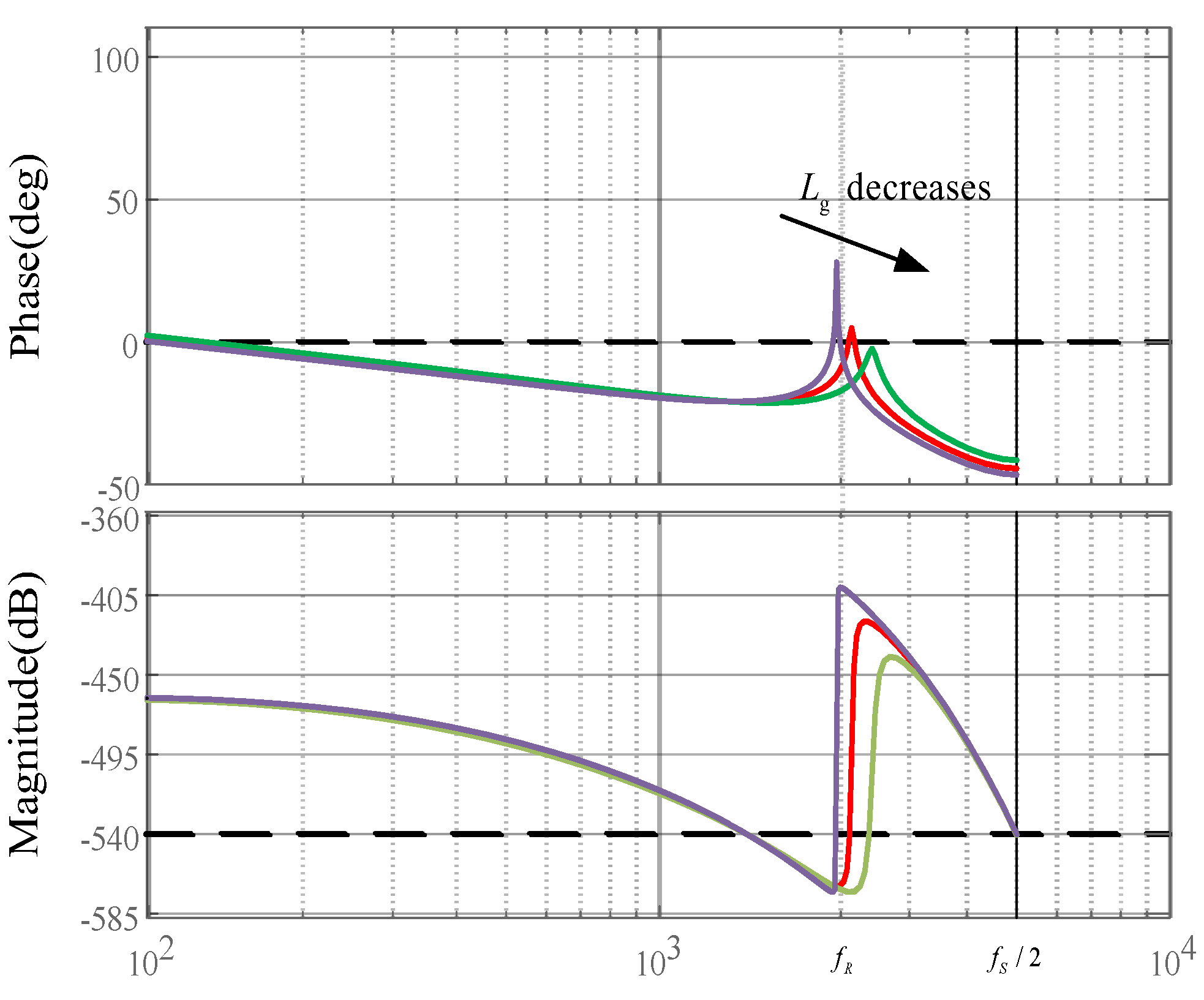
Affected by the digital control delay, the efficient damping area using the uncompensated GCFAD system is only (0, fR) (fR ∈ (fs/6, fs/3)). In a weak grid environment, the narrower the effective damping range, the poorer the system robustness.
(2)
To reduce the adverse effect of the digital control delay, the current work introduces the phase overrun compensation to counteract the control delay. As a result, the system’s efficient damping area is expanded from (0, fR)(fR ∈ (fs/6, fs/3)) to (0, 0.45fs), and the wider effective damping range is more conducive to the LCL filter’s parameter design and the response to the grid impedance variations, thereby improving the system’s stability and robustness.
(3)
The stability of the highly robust GCFAD system is rigorously verified, and the optimal active damped feedback link parameters are obtained by combining the polar plots of the closed-loop system. The simulation outcomes confirm the efficiency of the presented approach.

Author Contributions

Writing—original draft, A.G.; writing—review and editing, Y.T.; funding acquisition, Y.T.; collection of information, H.Z. All authors have read and agreed to the published version of the manuscript.

Funding

This work was supported, in part, by the research on comprehensive utilization model of solar energy based on aggregation and frequency division (2022D01C364).

Data Availability Statement

Data will be made available on request.

Conflicts of Interest

The authors declare that they have no known competing financial interests or personal relationships that could have appeared to influence the work reported in this paper.

References

  1. Luo, R.; He, Y.; Liu, J. Research on the unbalanced compensation of delta-connected cascaded h-bridge multilevel SVG. IEEE Trans. Ind. Electron. 2018, 65, 8667–8676. [Google Scholar] [CrossRef]
  2. Ni, Z.; Narimani, M.; Zargari, N.R. Optimal LCL filter design for a regenerative cascaded h-bridge (CHB) motor drive. In Proceedings of the 2020 IEEE Energy Conversion Congress and Exposition (ECCE), Detroit, MI, USA, 11–15 October 2020; pp. 3038–3043. [Google Scholar]
  3. Zheng, F.; Wu, W.; Chen, B.; Koutroulis, E. An optimized parameter design method for passivity-based control in a LCL-filtered grid-connected inverter. IEEE Access 2020, 8, 189878–189890. [Google Scholar] [CrossRef]
  4. Liu, X.; Qi, Y.; Tang, Y.; Guan, Y.; Wang, P.; Blaabjerg, F. Unified active damping control algorithm of inverter for LCL resonance and mechanical torsional vibration suppression. IEEE Trans. Ind. Electron. 2022, 69, 6611–6623. [Google Scholar] [CrossRef]
  5. Ma, G.; Xie, C.; Li, C.; Zou, J.; Guerrero, J.M. Passivity-based design of passive damping for LCL-type grid-connected inverters to achieve full-frequency passive output admittance. IEEE Trans. Power Electron. 2023, 38, 16048–16060. [Google Scholar] [CrossRef]
  6. Naresh, P.; Anirudh, C.; Seshadri, V.; Kumar, S. Comparison of passive damping based LCL filter design methods for grid-connected voltage source converters. In Proceedings of the International Conference on Power, Instrumentation, Control and Computing (PICC), Thrissur, India, 17–19 December 2020; pp. 1–6. [Google Scholar]
  7. Zhao, H.; Wu, W.; Orabi, M.; Koutroulis, E.; Chung, H.S.-H.; Blaabjerg, F. A passive damping design method of three-phase asymmetric-LCL power filter for grid-tied voltage source inverter. In Proceedings of the 2023 IEEE Energy Conversion Congress and Exposition (ECCE), Nashville, TN, USA, 29 October–2 November 2023; pp. 94–98. [Google Scholar]
  8. Ji, K.; Pang, H.; He, Z.; Li, Y.; Liu, D.; Tang, G. Active/passive method-based hybrid high-frequency damping design for MMCs. IEEE J. Emerg. Sel. Top. Power Electron. 2021, 9, 6086–6098. [Google Scholar] [CrossRef]
  9. Zhao, N.; Wang, G.; Zhang, R.; Li, B.; Bai, Y.; Xu, D. Inductor current feedback active damping method for reduced DC-link capacitance IPMSM drives. IEEE Trans. Power Electron. 2019, 34, 4558–4568. [Google Scholar] [CrossRef]
  10. Han, Y.; Li, Z.; Yang, P.; Wang, C.; Xu, L.; Guerrero, J.M. Analysis and design of improved weighted average current control strategy for LCL-type grid-connected inverters. IEEE Trans. Energy Convers. 2017, 32, 941–952. [Google Scholar] [CrossRef]
  11. Zhang, H.; Wang, X.; He, Y.; Pan, D.; Ruan, X. A compensation method to eliminate the impact of time delay on capacitor-current active damping. IEEE Trans. Ind. Electron. 2022, 69, 7512–7516. [Google Scholar] [CrossRef]
  12. Upadhyay, N.; Padhy, N.P.; Agarwal, P. Grid-current control with inverter-current feedback active damping for LCL grid-connected inverter. IEEE Trans. Indus. Appl. 2024, 60, 1738–1749. [Google Scholar] [CrossRef]
  13. Pan, D.; Ruan, X.; Wang, X. Direct realization of digital differentiators in discrete domain for active damping of LCL-type grid-connected inverter. IEEE Trans. Power Electron. 2018, 33, 8461–8473. [Google Scholar] [CrossRef]
  14. He, Y.; Wang, X.; Ruan, X.; Pan, D.; Qin, K. Hybrid active damping combining capacitor current feedback and point of common coupling voltage feedforward for LCL-type grid-connected inverter. IEEE Trans. Power Electron. 2021, 36, 2373–2383. [Google Scholar] [CrossRef]
  15. Chen, W.; Zhang, Y.; Tu, Y.; Guan, Y.; Shen, K.; Liu, J. Unified active damping strategy based on generalized virtual impedance in LCL-type grid-connected inverter. IEEE Trans. Ind. Electron. 2023, 70, 8129–8139. [Google Scholar] [CrossRef]
  16. Li, S.; Lin, H. A capacitor-current-feedback positive active damping control strategy for LCL-type grid-connected inverter to achieve high robustness. IEEE Trans. Power Electron. 2022, 37, 6462–6474. [Google Scholar] [CrossRef]
  17. Xue, C.; Ding, L.; Wu, X.; Li, Y.; Song, W. Model predictive control for grid-connected current-source converter with enhanced robustness and grid-current feedback only. IEEE J. Emerg. Sel. Top. Power Electron. 2022, 10, 5591–5603. [Google Scholar] [CrossRef]
  18. Kraemer, R.A.S.; Carati, E.G.; Cardoso, R.; da Costa, J.P.; Stein, C.M.O. Virtual state damping for resonance suppression and robustness improvement in LCL-type distributed generation inverters. IEEE Trans. Energy Convers. 2021, 36, 1216–1225. [Google Scholar] [CrossRef]
  19. Liu, T.; Liu, J.; Liu, Z.; Liu, Z. A study of virtual resistor-based active damping alternatives for LCL resonance in grid-connected voltage source inverters. IEEE Trans. Power Electron. 2020, 35, 247–262. [Google Scholar] [CrossRef]
  20. Geng, Y.; Qi, Y.; Dong, W.; Deng, R. An active damping method with improved grid current feedback. Proc. CSEE 2018, 38, 5557–5567. (In Chinese) [Google Scholar]
  21. Wei, X.; Jinsong, K. Stability analysis of LCL type static synchronous compensator for distribution network considering the influence of digital control delay. J. Elect. Eng. 2017, 32, 205–216. (In Chinese) [Google Scholar]
  22. Lin, Z.; Ruan, X.; Zhang, H.; Wu, L. A generalized real-time computation method with dual-sampling mode to eliminate the computation delay in digitally controlled inverters. IEEE Trans. Power Electron. 2022, 37, 5186–5195. [Google Scholar] [CrossRef]
  23. Stojić, D.M.; Šekara, T.B. Digital resonant current controller for LCL-filtered inverter based on modified current sampling and delay modeling. IEEE J. Emerg. Sel. Top. Power Electron. 2022, 10, 7109–7119. [Google Scholar] [CrossRef]
  24. Wang, T.; Yao, W.; Li, C.; Yang, H.; Li, W. Aliasing suppression with negligible phase lag for multi-sampled LCL-type grid-tied inverter. IEEE Trans. Power Electron. 2023, 38, 12520–12535. [Google Scholar] [CrossRef]
Figure 1. System structure of the LCL-type cascaded H-bridge SVG.
Electronics 14 00309 g001
Figure 2. Diagram of traditional GCFAD in continuous domain.
Electronics 14 00309 g002
Figure 3. Current loop equivalent control block diagram of conventional GCFAD.
Electronics 14 00309 g003
Figure 4. Frequency characteristics of Req and Xeq under digital control delay.
Electronics 14 00309 g004
Figure 5. The equivalent virtual impedance circuit. (a) 0 < f < fx1 or fx2 < f < fs/2, (b) fx1 < f < fx2.
Electronics 14 00309 g005
Figure 6. Bode diagram of the loop gain TD(s) for various grid impedances.
Electronics 14 00309 g006
Figure 7. Block diagram of the highly robust GCFAD system in the continuous domain.
Electronics 14 00309 g007
Figure 8. Frequency characteristics of Gc(z) for various values of m.
Electronics 14 00309 g008
Figure 9. Frequency characteristics of the highly robust GCFAD Req1 for various values of m.
Electronics 14 00309 g009
Figure 10. The polar plot of the closed-loop system for various values of the compensation coefficient m.
Electronics 14 00309 g010
Figure 11. System control block diagram in the z-domain.
Electronics 14 00309 g011
Figure 12. Closed-loop polar plot of the system for various values of the feedback coefficient KH. (a) Pre-compensation; (b) post-compensation.
Electronics 14 00309 g012
Figure 13. Closed-loop polar plot of the system versus the cutoff frequency ωd.
Electronics 14 00309 g013
Figure 14. A-phase waveform simulation before and after compensation. (a) Conventional GCFAD A-phase GC voltage and current. (b) Highly robust GCFAD A-phase GC voltage and current. (c) Highly robust GCFAD A-phase current THD.
Electronics 14 00309 g014
Figure 15. Simulation waveforms of the highly robust GCFAD A-phase for various grid impedance values. (a) Phase A GC voltage and current at Lg = 5.31 mH. (b) Phase A GC voltage and current at Lg = 10.62 mH. (c) THD of phase A GC current at Lg = 5.31 mH. (d) THD of phase A GC current at Lg = 10.62 mH.
Electronics 14 00309 g015
Figure 16. Dynamic response process of the GCFAD A-phase grid-connected current with high robustness to load mutation for various grid impedance values. (a) Lg = 0 mH. (b) Lg = 5.31 mH. (c) Lg = 10.62 mH.
Electronics 14 00309 g016
Table 1. The GC system parameters.
ParameterSymbolValue
Grid voltage (RMS)ug10,000 V
Fundamental frequencyf050 Hz
Rated capacity of the deviceS±10 Mvar
Submodule switching frequencyfSM1000 Hz
Number of submodulesN10
DC input voltageUdc1500 V
DC side capacitanceCdc3000 μF
Filter capacitanceC3.86 μF
SVG-side inductanceL13.5 mH
Grid-side inductanceL21.5 mH
Equivalent switching frequencyfsw10 kHz
Sampling ratefs10 kHz
Proportional gainKp0.316
Integral gainKi19.85
RMS: root mean square, fsw = N × fSM.
Disclaimer/Publisher’s Note: The statements, opinions and data contained in all publications are solely those of the individual author(s) and contributor(s) and not of MDPI and/or the editor(s). MDPI and/or the editor(s) disclaim responsibility for any injury to people or property resulting from any ideas, methods, instructions or products referred to in the content.

