Article

FPGA Accelerated Large-Scale State-Space Equations for Multi-Converter Systems

1
School of Electronic Science and Engineering, Southeast University, Nanjing 211189, China
2
School of Electrical Engineering, Southeast University, Nanjing 211189, China
3
Department of Computing, Imperial College London, London SW7 2AZ, UK
4
State Key Laboratory of Digital Sensing and Processing IC Technology, Nanjing 211189, China
*
Author to whom correspondence should be addressed.
Electronics 2025, 14(19), 3966; https://doi.org/10.3390/electronics14193966
Submission received: 28 August 2025 / Revised: 27 September 2025 / Accepted: 29 September 2025 / Published: 9 October 2025

Abstract

The increasing integration of high-frequency power electronic converters in renewable energy-grid systems has escalated reliability concerns, necessitating FPGA-accelerated large-scale real-time electromagnetic transient (EMT) computation to prevent failures. However, most existing studies prioritize computational performance and struggle to achieve large-scale EMT computation. To enhance the computational scale, we propose a scalable hardware architecture comprising domain-specific components and data-centric processing element (PE) arrays. This architecture is further enhanced by a graph-based matrix mapping methodology and matrix-aware fixed-point quantization for hardware-efficient computation. We demonstrate our principles with FPGA implementations of large-scale multi-converter systems. The experimental results show that we set a new record of supporting 1200 switches with a computation latency of 373 ns and an accuracy of 99.83% on FPGA implementations. Compared to the state-of-the-art large-scale EMT computation on FPGAs, our design on U55C FPGA achieves an up-to 200.00× increase in the switch scale, without I/O resource limitations, and demonstrates up-to 71.70% reduction in computation error and 51.43% reduction in DSP consumption, respectively.

1. Introduction

The dramatic increase in high-frequency power electronic converters at renewable energy-grid interfaces has exposed reliability issues, where converter failures have been recognized as major contributors to power outages [1,2]. This escalating challenge underscores the requirement for large-scale real-time electromagnetic transient (EMT) computation in multi-converter systems to prevent potential failures and maintain grid stability [3,4]. The critical challenges originate from the requirement to solve time-varying state-space equations through intensive iterations while meeting sub-microsecond latency requirements [5,6,7,8], which has prompted significant research efforts toward FPGA-accelerated EMT computation [9,10,11].
Previous FPGA-based implementations of EMT computation for converter systems mainly focus on optimizing accuracy, latency, and computational burden [10,12,13]. To reduce accumulation errors when solving state-space equations of converter systems, Ma et al. have proposed adaptive mixed-precision schemes to balance numerical accuracy and computational resource cost [12]. Zheng et al. have developed a semi-implicit parallel leapfrog approach to halve latency through interleaved parallel acceleration [10]. Mirzahosseini et al. have proposed a switching network partitioning (SNP) method that allows reducing computational overhead for the iteration of EMT, supporting up to four-converter systems [13]. Although these implementations have achieved superior performance in errors, latency, and workload reduction, they overlook the scalability of computational architecture for current increasingly large-scale multi-converter systems. Additionally, as the system scale expands, computational resource consumption and data transfer bandwidth will inevitably become critical bottlenecks for the system scalability.
To address these limitations and achieve large-scale EMT computation for multi-converter systems, this work aims to accelerate large-scale state-space equations on FPGAs with scalable hardware architecture and hardware-software (HW-SW) co-design optimizations, as illustrated in Figure 1. State-space equations are selected over nodal analysis for characterizing multi-converter systems due to their high-order discretization techniques improving EMT accuracy, coupled with recent advancements in automated matrix generation methods to efficiently handle switches [14,15,16]. The detailed contributions in this article are summarized as follows.
  • We propose a scalable hardware architecture for EMT computation in multi-converter systems, which employs data-centric PE arrays and domain-specific components to enable large-scale state-space equation acceleration via bandwidth optimizations.
  • We introduce an automated graph analysis and matrix-aware fixed-point quantization method to realize hardware–software co-design, translating state-space equations to weighted digraphs with priority (WDP) and generating stored matrices and data flows.
  • We develop an FPGA-accelerated large-scale multi-converter computation system on the AMD Alveo U55C platform. Our experimental results demonstrate a 200.00× scale increase in hardware acceleration, able to compute 1200 switches in 373 ns latency and 99.83% accuracy, compared to the state-of-the-art FPGA implementations.

2. Background and Motivations

This section presents the fundamental principles of EMT computation for multi-converter systems based on state-space equations and summarizes the characteristics of existing FPGA implementations. We focus on critical challenges in the design of large-scale EMT computation architecture. Table 1 presents a summary of variables involved in the rest of the article.

2.1. Multi-Converter Systems

This section introduces the topologies of multi-converter systems, including a three-phase and two-level voltage source converter (VSC) and a radial multi-converter system [17], where specific circuit architectures have been discussed in details in prior works [17].
The topology of a three-phase and two-level voltage source converter is characterized by a three-phase voltage source (i.e., u a , u b , and u c ) connected to line loads (i.e., resistances R a , R b , R c and inductances L a , L b , L c ), as well as grounded capacitors (i.e., C 1 and C 2 ) and a converter load resistor R l o a d . It incorporates six high-frequency switches (i.e., S 1 , S 2 , S 3 , S 4 , S 5 , and S 6 ), along with PWM signals for controlling the switches to adjust the converted voltage and current [18,19].
The radial multi-converter system consists of multiple converters connected to the grid with line loads R g and L g , where the alternating-current (AC) part is decoupled from the direct-current (DC) side [17].

2.2. State-Space Equations

This section describes the process of transforming converter topological circuits into the state-space equations.

2.2.1. Equation Derivation

The transformation begins by applying the binary resistor model to the power switches in a VSC [20], where each switch state corresponds to either R on = 0.005 Ω or R off = 1 × 10 6 Ω . For switch S i (i = 1, 2, …, 6), let R i represent its instantaneous resistance. The complementary operation of switch pairs ( S 2 k 1 , S 2 k ), where k = 1, 2, 3, ensures the invariant condition R 2 k 1 + R 2 k = R sum = R on + R off throughout the switching cycle.
The state-space equations are derived by expressing inductor voltages and capacitor currents through their respective state variable derivatives. Taking branch a as an instance, Kirchhoff’s voltage law yields the inductor current equation, as described in Equation (1).
L a d i a ( t ) d t = u a ( t ) R a + R 1 ( t ) R 2 ( t ) R sum i a ( t ) R 2 ( t ) R sum u c 1 ( t ) + R 1 ( t ) R sum u c 2 ( t )
Similarly, for capacitor voltage u c 1 , it is derived into Equation (2). The capacitor C 1 voltage u c 1 similarly follows from current conservation, as depicted in Equation (2).
C 1 d u c 1 ( t ) d t = R 2 ( t ) R sum i a ( t ) + R 4 ( t ) R sum i b ( t ) + R 6 ( t ) R sum i c ( t ) 1 R load + 3 R sum ( u c 1 ( t ) + u c 2 ( t ) )
Let vector x ( t ) = [ u c 1 ( t ) , u c 2 ( t ) , i a ( t ) , i b ( t ) , i c ( t ) ] T , vector u ( t ) = [ 0 , 0 , u a ( t ) , u b ( t ) , u c ( t ) ] T and state vector x ˙ ( t ) = [ d u c 1 ( t ) d t , d u c 2 ( t ) d t , d i a ( t ) d t , d i b ( t ) d t , d i c ( t ) d t ] T . We define matrix A ( t ) to represent the time-varying coefficients of the vector x ( t ) . By rearranging the inductance and capacitance terms from the left-hand side of Equations (1) and (2) to the right-hand sides, we obtain B as the coefficient matrix for the vector u ( t ) . We then can derive the state-space equation in Equation (3), where A ( t ) and B are 5 × 5 matrices, respectively [21,22,23].
x ˙ ( t ) = A ( t ) x ( t ) + B u ( t )

2.2.2. Numerical Integration Transformation

The state-space equation in Equation (3) admits an analytical solution in Equation (4), where x ( t 0 ) represents the initial state vector [8,24]. The analytical solution consists of a matrix exponential term and an integral term. However, the time-varying feature of the matrix A ( t ) and the presence of computation-intensive matrix exponential and integral operations impose significant computational challenges.
x ( t ) = e A ( t ) ( t t 0 ) x ( t 0 ) + t 0 t e A ( t ) ( t τ ) B u ( τ ) d τ
To mitigate computational burden, numerical integration methods have been proven more efficient for solving such issues. Taking the trapezoidal integration method as an example, we consider the differential equation d x d t = f ( x ( t ) , t ) . The trapezoidal integration equation is given by Equation (5), where f ( x ( t ) , t ) represents the integrand function. The Δ t represents the discretized time step.
x ( t + Δ t ) = x ( t ) + f ( x ( t ) , t ) + f ( x ( t + Δ t ) , t + Δ t ) 2 Δ t
Let K ( t ) = ( I 0.5 Δ t A ( t + Δ t ) ) 1 , P ( t ) = I + 0.5 Δ t A ( t ) , W = 0.5 Δ t B . We then substitute f ( x ( t ) , t ) = A ( t ) x ( t ) + B u ( t ) into Equation (5) and obtain the discrete equation in Equation (6).
x ( t + Δ t ) = K ( t ) P ( t ) x ( t ) + K ( t ) W ( u ( t ) + u ( t + Δ t ) )

2.2.3. Large-Scale State-Space Equations for Multi-Converter Systems

Equation (6) describes the behavior of a single converter through a 5 × 5 system matrix. However, if the number of converters increases to N, the matrix dimension will expand to ( 8 N 3 ) × ( 8 N 3 ) , resulting in quadratic computational complexity. To address this challenge in large-scale multi-converter systems, decoupling methods are essential.
Recent state-of-the-art work has proposed a decoupling method to reduce computational burden and enable parallel acceleration [17]. By utilizing historical inductor currents and capacitor voltages, the large-scale multi-converter system is partitioned into two subsystems. AC-side subsystem is governed by inductor-related current equations, and the other is described by capacitor-related voltage equations. As depicted in Equation (7), the decoupled equations allow for parallel acceleration of multiple converters in a multi-converter system, where x 1 ( t ) = [ u c 1 ( t ) , u c 2 ( t ) , ] T and x 2 ( t ) = [ i a ( t ) , i b ( t ) , i c ( t ) , ] T .
x 1 ( t + Δ t ) x 2 ( t + Δ t ) = D ( t ) x 1 ( t ) x 2 ( t ) + G ( t ) u 1 ( t ) u 2 ( t ) + F u 1 ( t + Δ t ) u 2 ( t + Δ t )
In this article, we aim to utilize Equation (7) to accelerate large-scale multi-converter systems and design a scalable hardware architecture on FPGAs.

2.3. Existing FPGA-Accelerated Implementations

With the advancement of semiconductor technology, the switching frequency of power devices in converters has exceeded 100 kHz [25]. This necessitates dynamic characteristic reconstruction with a temporal resolution of 1/50 to 1/100 of the switching period, requiring computational time steps to be reduced to the 100-nanosecond level [11]. Consequently, to accurately capture high-frequency switching characteristics in converter systems, existing FPGA-accelerated implementations have primarily focused on reducing latency, errors, and computational overhead [10,11,12,13,21,25,26,27,28,29,30,31,32,33,34,35].

2.3.1. Latency Minimization for Real-Time EMT Computation

Milton et al. proposed a latency-based linear multi-step compound method (LB-LMC) that exploits small time-steps to decouple nonlinear component solutions from system simulations, eliminating CPU-induced latency [25]. Through utilizing the particular simplification in the predictor step, Liu et al. designed a predictor–corrector circuit to achieve low latency [26]. Further utilizing the characteristics of interleaved computation, Zheng et al. developed a semi-implicit parallel leapfrog (SPL) method to halve latency while retaining the maximum error at 2.08% [10]. To meet real-time requirements, Xu et al. proposed a sub-microsecond level real-time simulation method through replacing converters with fixed-admittance matrices [27].

2.3.2. Error Suppression for High-Fidelity Transient Reconstruction

Silva et al. [28] incorporated floating-point arithmetic into FPGA designs and systematically evaluate state-equation solvers, including the Euler, improved Euler, and Runge–Kutta methods, to balance between computational precision and efficiency. Wang et al. [21] further enhanced computation accuracy by developing both generalized associated discrete circuit (G-ADC) and L/C-based associated discrete circuit (L/C-ADC) models, which minimize virtual power losses through strategic exploitation of parameter space stability regions. Refs. [29,30] proposed the initial error correction (IEC) method and initial error modification (IEM) method, both employing error compensation algorithms and DSP multiplexing architectures to degrade inaccuracies. Guo et al. [31] and Zhao et al. [32] introduced a signal-to-noise ratio (SNR) evaluation framework for state-space solver quantization, while Li et al. [33] achieved a remarkable 1.51% error reduction through their interpolation technique.

2.3.3. Computational Overhead Reduction for Efficient Iteration

To reduce computational overhead, TA-MP solver utilized a division of large matrices to construct an effective equation iteration with 93.00% LUT reduction [11]. Yang et al. proposed a delay-free decoupling method to compact and parallelize the discrete state-space equations [34]. Through balancing accuracy and time steps, Xu et al. developed a switching-period-synchronization-based (SPS) real-time EMT computation method to reduce the computation burden in unit time [35]. To degrade the computation burden of time-variant and large admittance matrices in each time step, Mirzahosseini et al. proposed a switching-network partitioning (SNP) method and enabled parallel network-component solutions, achieving sub-microsecond time steps [13].

2.4. Challenges and Motivations

The analysis of electromagnetic transients in power systems facilitates the prevention of operational failures, enhances grid stability, and mitigates privacy leakage risks stemming from electromagnetic transient characteristics [3,4,36,37]. However, with the dramatic increase in grid-connected renewable energy devices, the computational scale of EMT computation for multi-converter systems has emerged as the primary bottleneck, shifting focus away from solely considering the performance and simulation accuracy of the single converter [17,38,39].
To promote the scalability of FPGA-accelerated EMT computation, existing studies primarily focus on partitioning multi-converter systems into parallelizable subsystems for improving computational efficiency [13,17,38,39]. Most existing implementations rely on floating-point multiply-accumulate units (FPMACCs) for matrix-vector multiplications (MVMs), facing hardware resource constraints [13]. To mitigate these limitations, Milton et al. proposed a decentralized LB-LMC decomposition method that eliminates the need for a central solver, enabling multi-FPGA execution at the cost of communication overhead with supporting up to six converters [38]. However, these approaches struggle to fully leverage scalable hardware optimizations due to inherent architectural limitations. The dramatic surge in hardware resource consumption arises from an inefficient computational architecture that poorly accommodates system expansion. Additionally, as complexity scales, optimizing the mapping of computational matrices to hardware circuits emerges as a critical challenge in achieving large-scale EMT computation.
Consequently, this article is aimed at improving FPGA-implemented hardware computation architecture with hardware–software co-design optimizations to achieve large-scale EMT computation for multi-converter systems.

3. Hardware Architecture

Based on previous analysis, existing studies have faced the critical challenge of scalable design for large-scale multi-converter systems. To solve these issues, this section presents our proposed scalable hardware architecture on FPGAs. We focus on customized design of state-space equation computation for multi-converter systems, along with bandwidth optimization techniques.

3.1. Architectural Overview

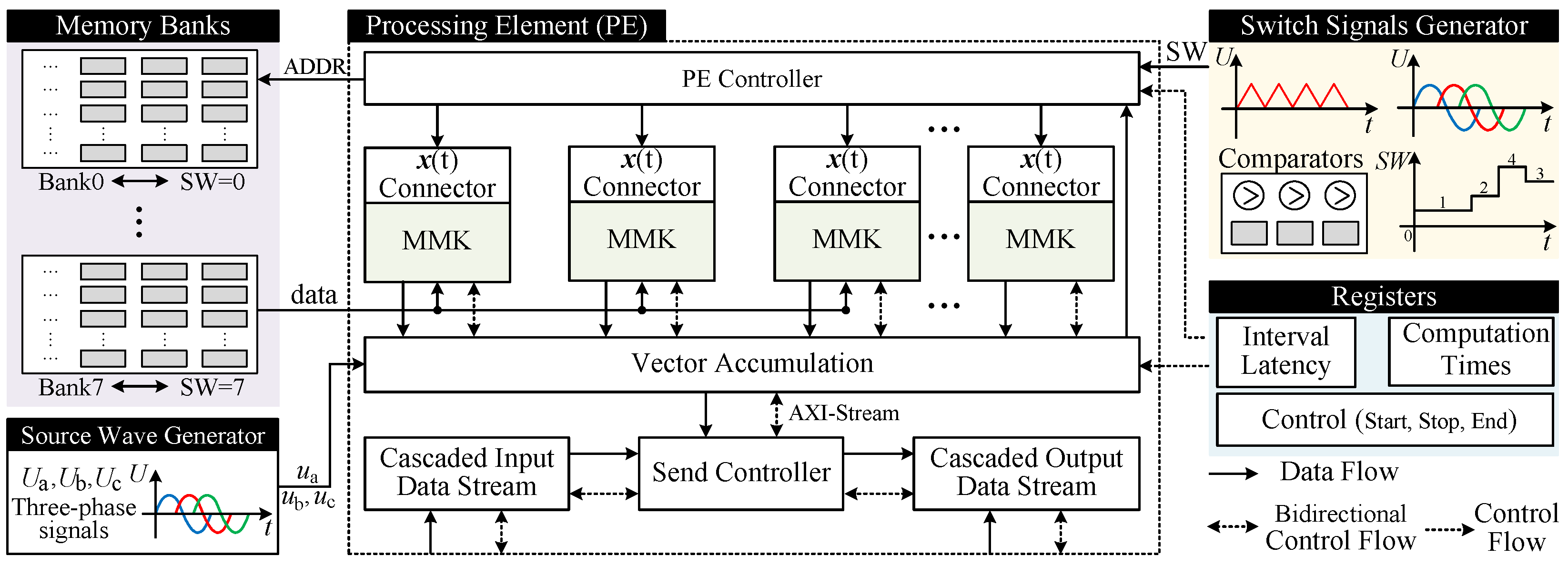
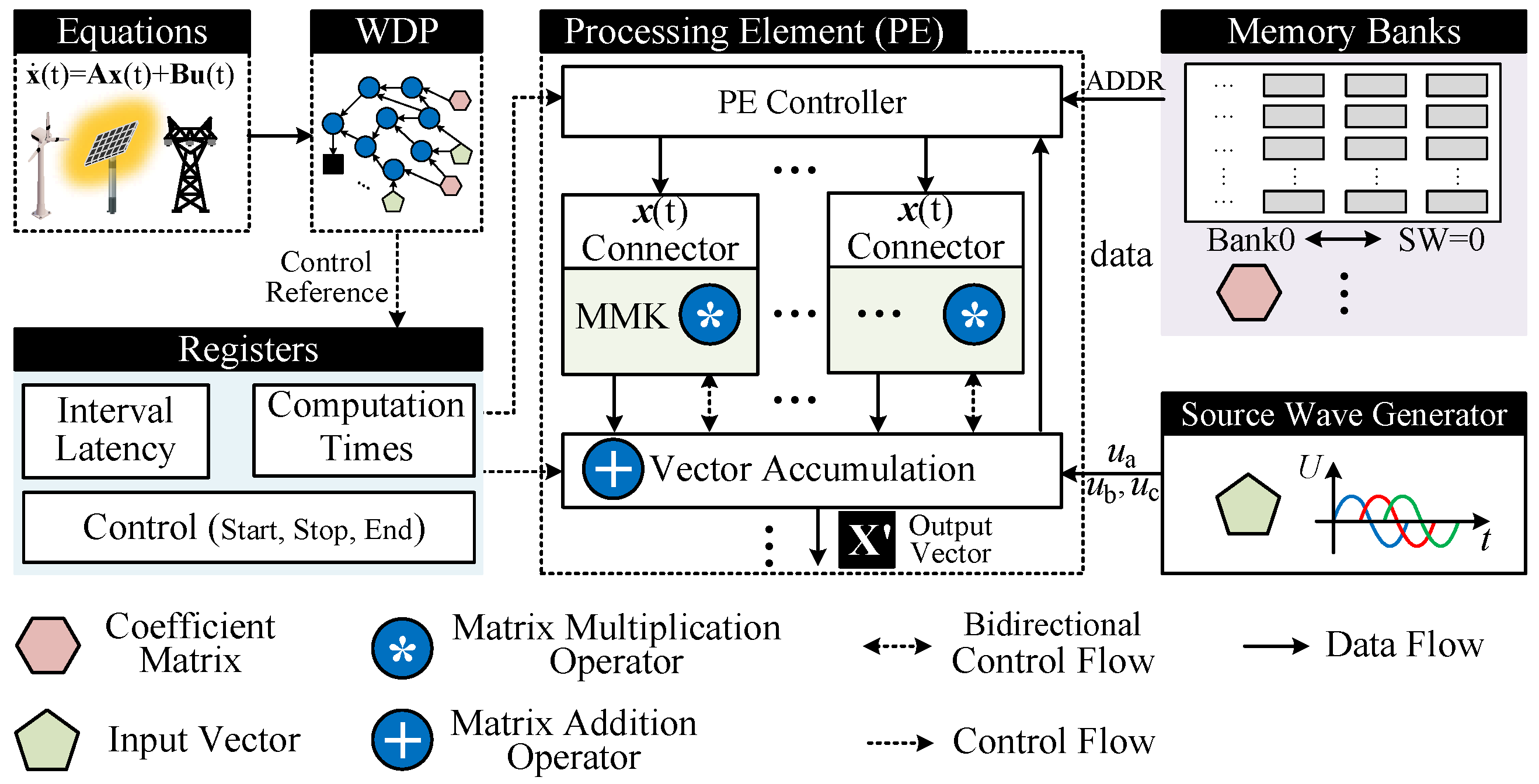
Figure 2 presents our proposed hardware architecture, which consists of a data-centric accelerator and a configuration module. The data-centric accelerator incorporates a PE array, memory banks, an AXI-Stream aggregation module, a controller, register sets, and customized generators for multi-converter systems including switching signal generators, carrier wave generators, and source wave generators. The PE array is dedicated to matrix computation for state-space equations. The memory banks store time-varying coefficient matrices required by these equations. The AXI-Stream aggregation module arbitrates and consolidates computed data streams before transmitting them to the configuration module. The controller receives configuration instructions and parameter inputs, subsequently coordinating computational tasks across other modules. In power systems, carrier and source waves serve as specialized modulation signals for switching control signals, where varying wave parameters yield different switching control curves. The switching signal generator primarily selects time-varying coefficient matrices in state-space equations, such as K ( t ) in Equation (6) and D ( t ) in Equation (7).
The configuration module manages both accelerator parameterization and data interaction. The architecture demonstrates deployment flexibility across advanced accelerator cards (e.g., Alveo U55C FPGA) and traditional FPGA (e.g., XCKU060). Within this design, components positioned to the right of the finite state machine (FSM) controller constitute an optional implementation path. The data truncation with DAC output enables physical-layer interactive computation for experimental validation of system feasibility and operational integrity. Conversely, utilizing the other part CPU-FPGA heterogeneous computing configuration highlights the scalability, since I/O resource constraints fundamentally limit the maximum implementable scale.

3.2. Domain-Specific Components for Multi-Converter Systems

Figure 3 presents the customized component design for EMT computation in multi-converter systems, comprising a carrier wave generator, a source wave generator, and a switch signals generator.
As shown in Figure 3a, the carrier wave generator module incorporates a waveform RAM that enables configurable settings, including waveform parameters and decimal point positioning. By default, the RAM stores triangular wave signals. During operation, the output frequency can be modulated by configuring the address step size. Upon receiving an external read signal, the FSM coordinates the address decoder to perform incremental address adjustment. Once the RAM read address is determined, the retrieved waveform data is fed into a bit sign-extension module to prevent decimal point misalignment beyond the sign bit position. An adaptive truncation module adjusts the decimal point position through data shifting, and the processed waveform data is transmitted via a TX module along with a synchronized data valid signal.
The source wave generator module follows a similar implementation, as depicted in Figure 3b. Considering the potential X-axis symmetry in periodic waveforms (e.g., sine waves), the embedded RAM can store the positive half-cycle data to optimize memory utilization. After data retrieval, a bit flip module inverts the data when operating in the negative half-cycle, as determined by the sign detection.
The switch signal generator module primarily produces the control signals SW[2:0] for the switch pairs S 1 S 2 , S 3 S 4 , S 5 S 6 . Control signals SW[0], SW[1], and SW[2] typically exhibit PWM-like waveforms. The signals are derived from phase-shifted comparisons between carrier and source waves, implemented via an array of comparators within this module, as shown in Figure 3c.

3.3. Data-Centric PE Array

The computation of state-space equations primarily involves matrix–vector multiplication and accumulation operations. Unlike conventional matrix computation, the coefficient matrices in multi-converter systems are time-varying and each calculation depends on the previous result, introducing challenges for parallel implementation. Since the coefficient matrices change after each iteration, we propose a data-centric processing element (PE) array augmented with customized memory mapping to address these limitations.
For multi-converter systems utilizing state-space modeling, the number of coefficient matrices of each converter is finite owing to the constant admittance method [17]. These matrices can thus be pre-stored in memory under a structured addressing scheme. As depicted in Figure 4, the matrix–vector multiplication workflow employs a dedicated memory-mapping strategy. Given an m × n coefficient matrix with a data width of q bits, each column vector is extracted, indexed in ascending order, and concatenated into a q m -bit word. These column vectors are stored sequentially, with each memory address mapping to one full column. The coefficient matrices are organized in memory according to the switching state SW[2:0], where the first n addresses contain the matrix for SW = 0 and the subsequent n addresses for SW = 1. During computation, the SW value determines the base address for matrix retrieval. Each decoded column vector ( a 1 j , a 2 j , , a m j ) T is multiplied element-wise with the state vector ( x 1 , x 2 , , x n ) T , and the products are accumulated to yield the output for the current timestep.
Figure 5 provides a concrete workflow example for a 4 × 1 state vector x ( t ) . As shown in Figure 5a, memory banks distribute matrices according to SW values. SW = 0 matrices reside in bank0 and SW = 1 matrices in bank1 with contiguous address linkage. For the computational core, we implement two architectures with supporting fully parallel and pipelined computation, respectively. The fully parallel design computes all four scalar multiplications and accumulations per clock cycle, achieving ultra-low latency at high resource cost. In contrast, the pipelined computation reuses a single multiplier-accumulator pair and processes one scalar operation per cycle to reduce resource overhead, resulting in 5.00 × higher latency scaling with state vector dimension.
Building upon the aforementioned functional analysis, the subsequent sections present detailed design descriptions, encompassing the fundamental components of the matrix multiplication kernel, the processing element (PE), and the data-centric PE array.

3.3.1. Matrix Multiplication Kernel

The matrix multiplication kernel (MMK) architecture integrates seven fundamental components, including a column vector receiver module for data input, a configurable column vector shifter, a multiplier–adder pair computation array, a accuracy-aware data truncation module, a column vector transmitter module for result output, a handshake controller for flow regulation, and a y ( t ) connector for data exchanging. This design supports a resource-efficient pipelined mode and a high-performance fully parallel mode. As depicted in Figure 6, the pipelined implementation employs temporal reuse of a single multiplier-adder pair through careful scheduling. The parallel configuration activates all computational units simultaneously to minimize latency with proportional increases in resource consumption. The subsequent description details the functional interactions and execution sequence of these components.
The computation process initiates when the PE controller transfers data through the x ( t ) connector while simultaneously prefetching the coefficient matrix column vectors corresponding to the current SW from memory banks. Upon receiving both the x ( t ) connector data and coefficient matrix column vectors, the column vector receiver module decodes them into independent scalar data. These scalars are divided into input column vector signals ( x 1 , x 2 , x 3 , x 4 ) and coefficient matrix column vector signals ( a 1 j , a 2 j , a 3 j , a 4 j ) , which are then fed into respective column vector shifters. In pipelined mode, the shifters sequentially output one x i and a kj pair per cycle for multiplication operations, where i , k { 1 , 2 , 3 , 4 } . This generates 16 possible combinations following the sequence ( x 1 , a 11 ) , ( x 2 , a 12 ) , ( x 3 , a 13 ) , ( x 4 , a 14 ) , ( x 1 , a 21 ) , ( x 2 , a 22 ) , , ensuring systematic computation. In the fully parallel mode, the coefficient matrix shifter is replaced by D flip-flops, enabling simultaneous multiplication between each x i and all elements of the current coefficient matrix column, with all multiplier-adder pairs activated.
After computation, the intermediate results are automatically truncated according to the configured fractional precision, preventing bit-width growth in cascaded processing stages. The data truncation module selectively removes insignificant lower-order bits from the outputs ( y 1 , y 2 , y 3 , y 4 ) while retaining valid data for subsequent transfer. The column vector transmitter module then coordinates with the handshake controller to enforce ready-valid flow control, ensuring backpressure support. Concurrently with valid signal assertion, the final y ( t ) result is simultaneously transmitted via the y ( t ) connector module for further processing.

3.3.2. Processing Element Design

The processing element (PE) primarily executes converter equation computation by employing an array of the proposed MMKs. Structurally, each PE consists of an MMK array, a PE controller module, a vector accumulation module, a cascaded input data stream module, a cascaded output data stream module, and a send controller module. For state-space equation computation, each iteration requires multiple matrix–vector multiplications and column vector additions. The MMK array handles parallel matrix–vector multiplications, while the vector accumulator performs intermediate column vector summation.
During operation, external registers first configure PE parameters including computation cycles and timing intervals. Upon receiving the start signal, the PE controller initiates computation. Simultaneously, the switch signal generator compares signals from the carrier wave generator and the source wave generator module to generate SW signals for memory address control, which are subsequently transmitted to the PE controller. The PE controller translates these SW signals into memory ADDR signals to fetch corresponding coefficient matrices. Subsequently, the controller schedules sequential matrix–vector multiplication across the MMK array, with results routed to the vector accumulation module for state vector generation. The output state vector undergoes arbitration with external PE data streams, where the send controller appends ID tags before forwarding to downstream PEs via cascaded output. The accumulated results from the vector accumulation module are also fed back to MMK inputs for iterative computation, as subsequent calculations depend on current outputs despite requiring intermediate transfers. Following each iteration, the source wave generator module sends updated three-phase signals u a , u b , u c to refresh the internal column vector u ( t ) and u ( t + Δ t ) in the vector accumulation module.
The cascaded data flow design with ID encoding in the PE alleviates bandwidth limitations for scalability, as large-scale EMT computation impose significant data transfer demands which we further analyze in the following section.

3.3.3. Bandwidth Optimizations Through Latency Insertion

The bandwidth limitation in large-scale implementations can be illustrated through a concrete example. Consider a system where each converter possesses four state variables, each represented by 16-bit precision. For a typical EMT computation with a 500 ns time step and 100 MHz clock frequency, the bandwidth requirement per converter would theoretically be ( 16 × 4 ) / 500 = 0.128 Gbps. However, this calculation underestimates actual demands since all converter states output simultaneously within the 500 ns window, with effective transfer occupying only a fraction of this period. Consequently, the instantaneous bandwidth surges to ( 16 × 4 ) / 10 = 6.4 Gbps per converter. When scaled to 100 converters, this leads to a peak bandwidth demand of 640 Gbps, while the average bandwidth remains at 12.8 Gbps. This presents the fundamental scalability challenge that simultaneous computation for multiple converters produces prohibitive instantaneous data transfer demands. Our analysis further reveals that bandwidth requirements grow linearly with computation scale. Practical EMT implementations typically require higher precision exceeding 16-bit and more state variables, exacerbating bandwidth constraints.
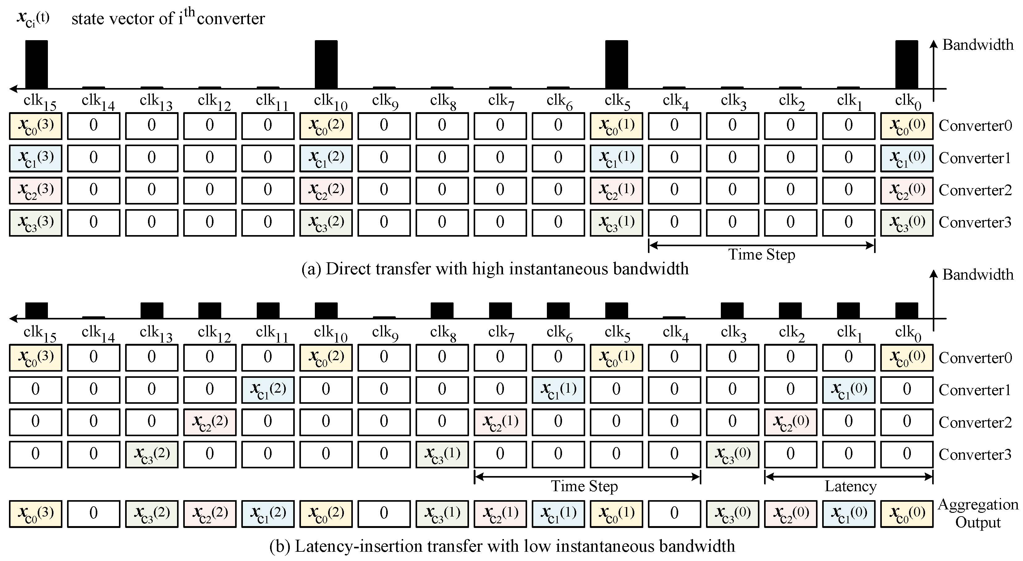
We observe that state-space equation iterations inherently incorporate multiple clock cycles denoted as Δ t between computation, where Δ t is also called time step in power system field. Assuming that we have four converters with Δ t = 4 , we provide an instance of different transfers in Figure 7. As shown in Figure 7a, direct implementations waste these intervals when processing multiple converters concurrently, causing the observed bandwidth spikes. Direct transfers of all computational results inevitably generate excessive instantaneous bandwidth. To address this issue, we propose a latency-insertion transfer method that effectively balances bandwidth utilization across computation intervals, as depicted in Figure 7b. This approach demonstrates a 75.00% reduction in peak bandwidth, where the reduction percent is related to Δ t and converter numbers. Theoretically, the maximum supported converter count becomes Δ t when organized in groups matching the computation interval duration. Given the necessary solving time constraint of state-space equations, if multiple converters are calculated simultaneously, a high concurrent data volume occurs in a single clock cycle which will violate the maximum bandwidth on board. Therefore, we implement a cascade PE array to address this issue, resulting in a balance of bandwidth and performance.
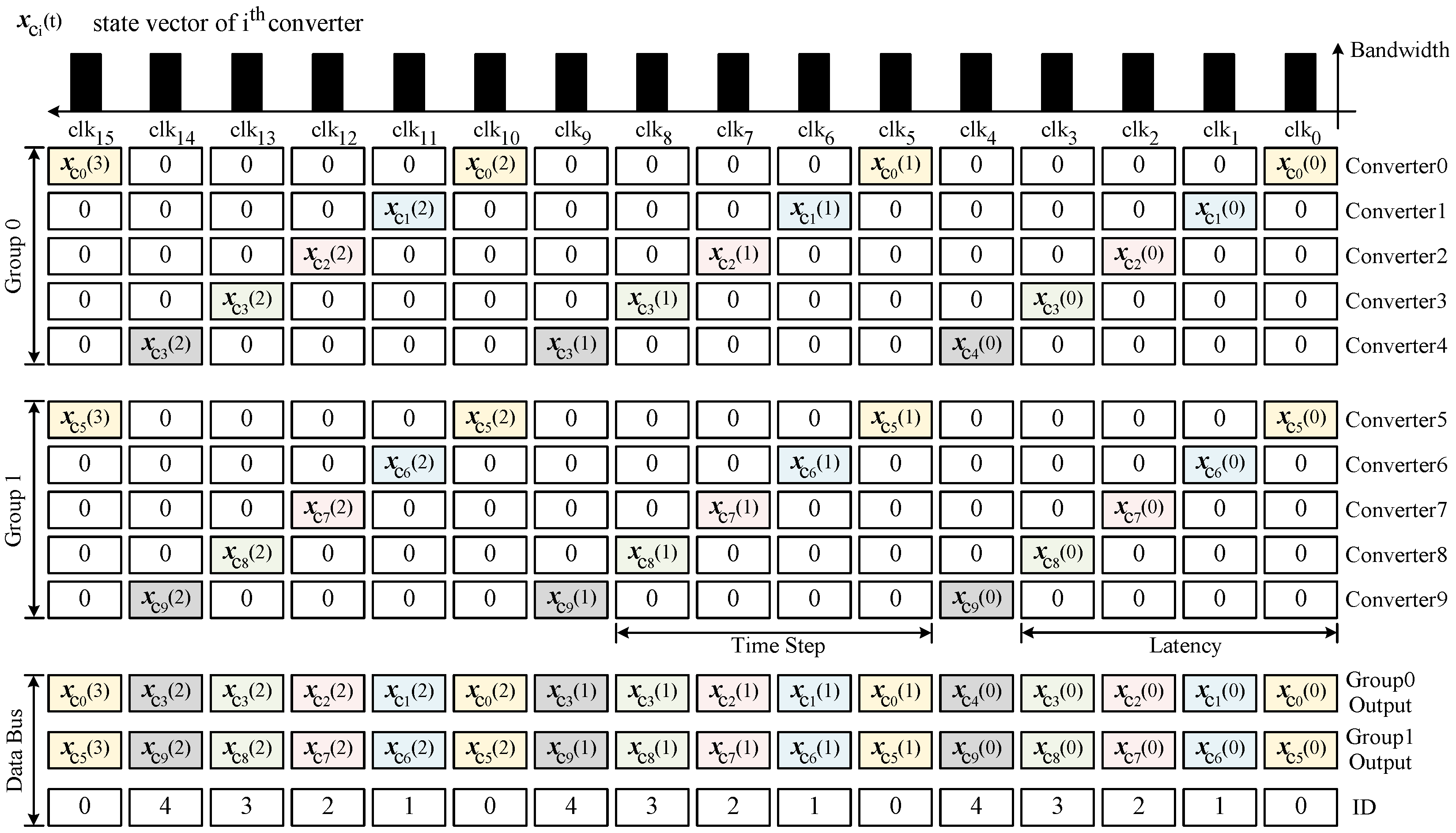
To further enhance the scalability, we utilize bus widths that surpass single converter data requirements. The system design parameterizes this optimization by defining the bus width as m bits, while each converter’s output requires n × w bits, where n represents the number of state variables and w denotes their bit width. Through this configuration, the maximum supported converter count scales according to N m a x = Δ t × m n w .
Figure 8 illustrates the final implementation of our proposed transfer scheme, which combines the latency-insertion method with optimized bus-width allocation. The results present bandwidth equalization, where the originally concentrated instantaneous data transfer is now evenly distributed across multiple clock cycles. To uniquely identify each transfer group, we allocate the remaining bus width to an identification (ID) field. This ID coding system provides unambiguous identification for converter output combinations. For instance, when ID = 0, the transmitted data contain x c 5 ( t ) and x c 0 ( t ) in descending order of bit significance. The scheme effectively resolves the bandwidth bottleneck while maintaining data integrity through this systematic grouping approach.
To provide a clearly explanation of our latency control implementation, we present the detailed workflow, as illustrated in Figure 9. During the initial Idle state, the controller configures dedicated registers with latency parameters for each PE. The system then enters the Configuration state, where the control module sequentially loads these parameters from the registers and distributes them to the cascaded PE array. In the Computation state, the control module initiates parallel processing via Valid-Ready handshaking protocols. Throughout execution, the latency control module regulates computational flow by precisely scheduling Ready signal assertions according to the preconfigured latency parameters. It enables fine-grained control of computation pause and resumption cycles.

3.3.4. Data-Centric Array Computation

To meet the aforementioned bandwidth optimization requirements, we have developed a data-centric computational architecture that constructs the mobile PE organization and data flow management. The architecture requires to ensure precise control of matrix computation within each PE, including computation cycles, delay insertion, and the capability to pause matrix-vector operations at any instance. As illustrated in Figure 10, these functionalities are implemented through a combination of external registers and internal control units within each PE. The PE array organization adopts a column-based grouping strategy, where multiple PEs form a computational cluster. The initial cascaded latencies are achieved through data flow propagation, with each PE equipped with dedicated cascade input and output modules that automatically insert single-cycle latencies during data forwarding operations. The multi-group data stream merging is accomplished through the final PE interactions, where an extended bus width incorporates additional group ID markers to facilitate subsequent verification. Furthermore, to accommodate multi-channel transfer scenarios (e.g., HBM interfaces), the PE array architecture supports expansion through parallel data channels. As illustrated in the left part of Figure 2, the PE array structure demonstrates the implementation of multi-PE grouping, multi-group merging, and multi-channel transfer scaling. External registers configure both the array-level control modules and internal PE parameters, including the predefined computation times and interval latency settings. The control module coordinates the execution of computational tasks across the PE array. Each processed data stream in the bottom row is automatically tagged with its corresponding PE ID before being forwarded to the subsequent row.
Upon receiving all data streams at the final row, the merging process initiates in a right-to-left sequence, where the leftmost PE within each merging group consolidates the complete data flow before transmitting it to the external AXI-Stream aggregation module. Upon completing computation, each result is forwarded without buffering. The architecture maintains continuous data flow across the entire PE array, effectively utilizing the temporal intervals between state-space equation iterations to maximize computational throughput and pipeline efficiency. This data-centric streaming ensures high transfer utilization while maintaining deterministic latency characteristics essential for large-scale computation.

4. Hardware–Software Co-Design Optimizations

This section introduces a systematic mapping scheme for deploying state-space equation coefficient matrices onto the proposed computational architecture. By integrating graph-based analysis and optimized quantization techniques, these approaches are employed to reduce design complexity and hardware resource requirements while minimizing computational accuracy degradation.

4.1. Graph-Based Analysis for State-Space Equations

Although the state-space equations in Equations (6) and (7) represent the complete system formulation, practical FPGA implementation necessitates matrix decomposition into smaller submatrices and vectors due to computational resource limitations in large-scale operations [11]. This decomposition introduces critical challenges in efficiently mapping the resulting components onto hardware architectures. Our approach exploits inherent mathematical equivalences and transformation patterns by representing matrix operations as graph nodes, effectively converting the mapping problem into a graph optimization framework. This section details both the graph-based analysis process and solution methodology.

4.1.1. Weighted Digraph with Priority

In the proposed method, the weighted digraph with priority (WDP) serves as the core component for graph optimization. This section provides the formal definitions and specifications. The proposed WDP is developed from the basic graph. A graph G is a pair G = ( V , E ) , where V is a set of vertices of the graph and E is a set of edges of the graph [40], as shown in Figure 11a.
To represent the importance of connections in the graph, the weighted graph adds a weight for each edge in graph, which can be denoted as G = ( V , E ) , where the set E consists of pair { p , q , w } . The { p , q , w } stands for an edge with the weight w from the vertex p to q, as depicted in Figure 11b. To indicate the direction of transition between the nodes in the graph, the digraph G introduces an arrow to represent the direction, as described in [40]. To simplify the description and eliminate the maps, we redefine E to be a set composed of the list [ p , q ] , where the list [ p , q ] stands for the edge with arrow from vertex p to vertex q. As shown in Figure 11b, the set E = {[1, 3], [1, 4], [2, 3], [3, 4], [3, 5], [4, 5]}, where [4, 5] means that the arrow starts from vertex 4 to 5. To make the digraph become hardware-friendly, we first introduce the parallelism consideration by priority to reform the digraph and allocate accuracy weight for each edge, where the same priority stands for the simultaneous calculation beginning when being deployed on FPGAs. The weight of each edge is regarded as the basis for adjusting a WDP.
The WDP is still defined as a pair G = ( V , E ) of sets of vertices, edges, and arrows together. The set E is defined as a list [ p , q , k ] with three sizes, where the list [ p , q , k ] represents the arrow starting from vertex p to vertex q with priority k, as shown in Figure 11d. To characterize the order of start points p 0 and p 1 accessing the end point q, we append the priority of arrows arriving at each vertex. As shown in Figure 11d, each arrow is equipped with a priority of calculation and a priority of access order.

4.1.2. Logic Equivalence Transformation to Simplify WDPs

A WDP encompasses critical computational performance metrics, including latency, resource utilization, and accuracy. The number of sets c in V directly reflects memory consumption due to coefficient matrix storage, while the root-to-end path length determines computational latency. Operator counts for additions and multiplications quantify arithmetic complexity, and node weights govern numerical precision.
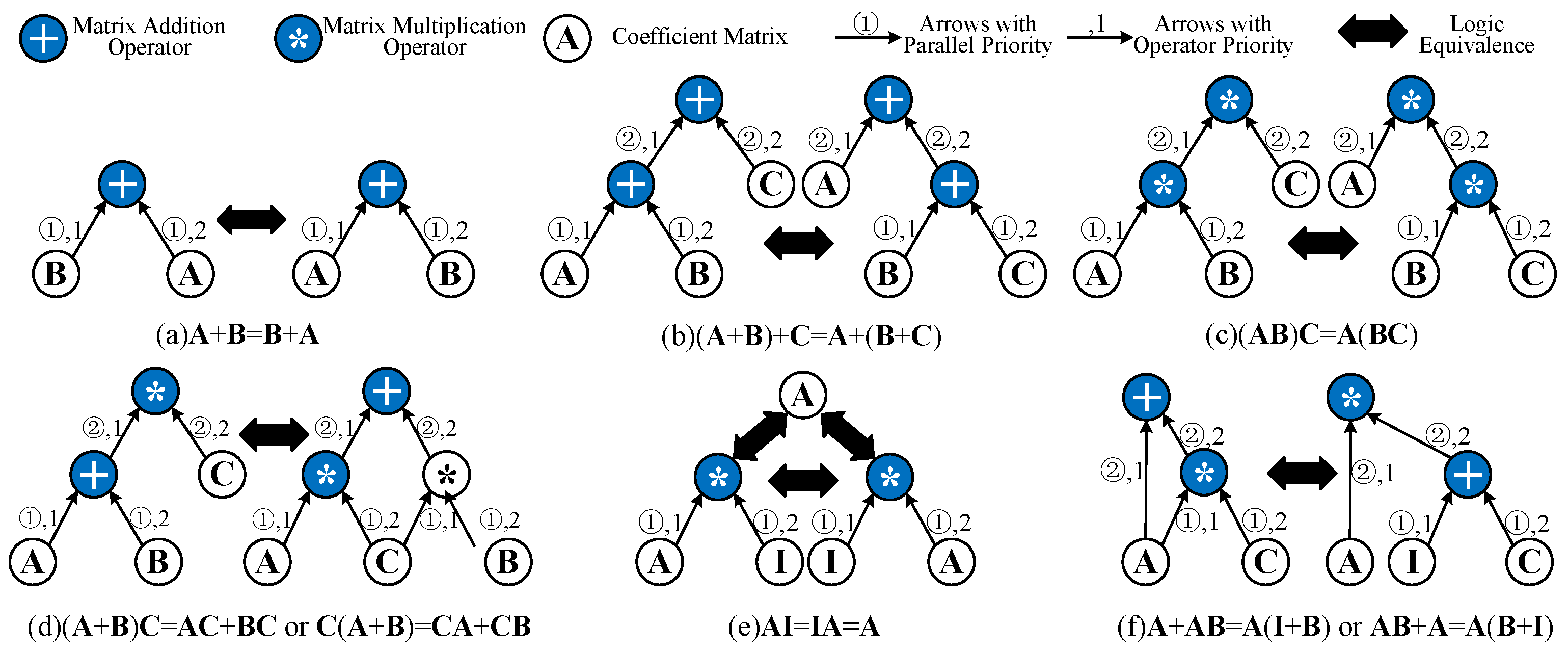
To optimize WDPs, we present the logical equivalence transformation method based on matrix operation laws, which enables node count reduction and computational paths simplification to minimize latency and resource overhead. The weights redistribution ensures precision preservation during structural refinement. Figure 12 introduces six equivalence rules, including commutative law of addition (CLA), associative law of addition (ALA), associative law of multiplication (ALM), distributive law of multiplication (DLM), elimination of the identity matrix (EIM) and introduction of the identity matrix (IIM).

4.1.3. WDP Setup, Simplification, and Mapping

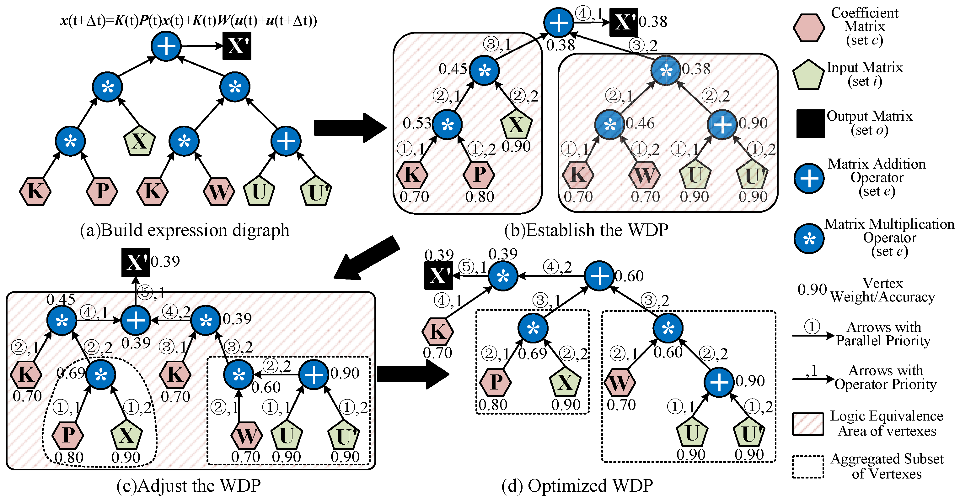
To demonstrate our WDP optimization method and its application to state-space equations, we take Equation (6) as an illustrative case. As shown in Figure 13a, we first construct an expression-directed graph that preserves the fundamental properties of the state-space representation, including matrix multiplication and addition operations, state variables, and time-varying input column vectors.
Based on Equation (6), we construct a WDP as a pair G = ( V , E ) , where the vertices V represent matrices and operators, and the directed edges E denote computational processes between these matrices and operators. Following the characteristics of state-space equations, we introduce a type attribute for the set V, which contains four vertex sets, i.e., the coefficient matrix set c, the input vector set i, the output vector set o, and the expression operator set e, i.e., V = ( c , i , e , o ) . Each subset is composed of a list [ n , w ] . To characterize weights in WDP, we define weight w as the average precision of each vertex matrix determined by quantization error. For an n × m matrix M with q-bit quantization, the average precision w can be calculated using the equation w = 1 n × m y M y × 2 q y × 2 q .
We then construct the WDP by assigning priorities and weights to the directed graph according to the matrix operation sequence and quantization parameters. As shown in Figure 13b, the output X is assigned the lowest parallel priority since it represents the final computational stage. Each operator node processes two inputs. For example, the multiplication operator takes K and P matrices as inputs, with the product subsequently multiplied by X . The operation priority determines the left-right execution order. In the KP multiplication, left operand K receives the highest priority 1 while right operand P is assigned secondary priority 2.
For a given WDP, as shown in Figure 13b, we employ the proposed logical equivalence method to optimize it. To avoid a local optimal solution from single-step optimization, we adopt a multi-step approach where each transformation considers potential subsequent steps up to R F iterations, ultimately selecting the globally optimal solution based on performance metrics. The step length R F is defined as the receptive field (RF). In Figure 13b, dashed and red-shaded regions represent aggregated subsets g m , g m + 1 , . . . , g n and logically equivalent subsets g s u b , respectively. When R F = 1 , the WDP in Figure 13b represents the optimal solution. Extending to R F = 2 yields the improved WDP in Figure 13c, where the ALM law from Figure 12c enables structural adaptation without graph simplification. Subsequent application of the DLM law derives the final topology, producing the optimized WDP in Figure 13d with reduced multiplicative operators compared to the initial configuration.
For the optimized WDP, we can directly map WDPs to the proposed hardware architecture. Figure 14 presents an instance of mapping a WDP to hardware modules. The quantized coefficient matrices are stored in memory banks through .coe files. The time-varying column vector matrix, consisting of three-phase voltages and zero elements, is assigned to the source wave generator module. Matrix multiplication operators are mapped sequentially to the MMK array in the PE, with each MMK handling a single matrix multiplication. If MMK resources are insufficient, external registers dynamically schedule computations to enable MMK reuse. Matrix addition operations are allocated to the vector accumulation module, which processes all matrix–vector additions. Finally, the output column vector from the vector accumulation module is transmitted via the AXI-Stream bus.
Beyond the demonstrated examples, our methodology can be extended to other state-space equations whose discretized form involves only matrix multiplications, additions, and subtractions. For such cases, we first construct an expression digraph based on the computational flow. Subsequently, we establish the WDP according to both the operation sequence and quantization parameters. The WDP is then optimized through logic equivalence transformations before being mapped onto our hardware architecture following the design flow presented in this section.

4.2. Matrix-Aware Fixed-Point Quantization Method

During solving discrete state-space equations for multi-converter systems, FPGA-accelerated implementations typically employ fixed-point quantization to optimize hardware resource utilization. The quantized coefficient matrices propagate through the entire iterative solving process, where accumulated quantization errors may cause a solution divergence if exceeding certain thresholds. This error amplification mechanism necessitates quantization analysis prior to implementation of large-scale state-space equations.
The coefficient matrices in multi-converter systems exhibit extreme numerical ranges spanning from 1 × 10 10 to 1 × 10 10 , primarily due to the physical properties of on-state and off-state resistances. This wide dynamic range poses significant challenges for fixed-point quantization. Conventional approaches face a fundamental trade-off. Although ultra-high-precision quantization (e.g., 64-bit) maintains numerical accuracy, it demands excessive memory and computational resources. Conversely, truncating extremely small values leads to zero elements in critical matrix positions, particularly along the diagonals. Such truncation disrupts numerical balancing during iteration, potentially destabilizing the entire solution process.
To resolve this issue, we propose a matrix-aware fixed-point quantization method incorporating mean absolute percentage error (MAPE) metric for precision evaluation. For matrix A m × n , the quantization error Γ is defined in Equation (8), where Q ( · ) denotes the quantization operator.
Γ = 1 m n i , j m , n A i j Q ( A i j ) A i j × 100.00 %
This method exploits the characteristic step-wise MAPE reduction observed in multi-converter matrices with increasing bit width, particularly noting a critical precision threshold where errors for extreme values become acceptable. The minimum quantization bit width Q m i n is determined through Equation (9).
Q min = arg min q Γ ( q ) ϵ min | A i j q | > ξ
The proposed matrix-aware fixed-point quantization method establishes a dual-parameter equation comprising a global error threshold (typically set at ϵ = 0.10%) and an element-wise tolerance ( ξ ) to effectively handle matrices with extreme numerical ranges. This approach fundamentally differs from conventional quantization techniques by explicitly incorporating matrix numerical characteristics into the bit-width selection process. Through sensitive to extreme numerical ranges, this method achieves concurrent optimization of computational stability and hardware efficiency. This is a critical requirement for FPGA-implemented EMT computation where numerical stability and resource constraints must be balanced.

5. Evaluation

5.1. Experimental Setup

Our proposed scalable hardware architecture is implemented on the AMD Alveo U55C and XCKU060 FPGA platforms to evaluate scalability and physical reliability. The hardware design is tested through the Vivado 2022.2 tool based on the Intel i9-14900K CPU. To validate the necessity of FPGA acceleration and verify the hardware results, we benchmark the same design on the i9-14900K CPU and the Nvidia RTX4090 GPU. The experimental FPGA platform is shown in Figure 15.

5.1.1. Workloads

A VSC circuit configuration shown in [17] is selected to evaluate the performance characteristics and resource utilization of the single converter. The radial multi-converter system depicted in [17] serves as the test case for assessing the scalability of large-scale systems. The corresponding parameter configurations for the converter are provided in Table 1. Each converter is characterized by a state vector of dimension 5.
The bit-width allocation for computational state vectors and fixed-point quantization parameters adhere to constraints derived from state-space equation solutions. Let w i n t denote the integer part bit-width and w f r a c represent the fractional part bit-width of the quantized state vectors. To satisfy the oscillation initiation condition for numerical integration methods, the product of input vector u ( t ) and its coefficient matrix in Equation (6) and Equation (7) are expected to yield a fixed-point and non-zero integer value. Otherwise, the numerical integration iteration would remain at zero.
The integer bit-width requirement is determined by the input voltage range, where the maximum amplitude of the input vector u ( t ) satisfies V r m s = 326 kV ( 2 9 , 2 9 ) , necessitating w i n t 10 bits to accommodate this dynamic range. For the fractional bit-width specification, we define T m as the minimum magnitude in the coefficient matrix. The T m can be calculated through the product of the time step Δ t with the minimal values of min { R o n , R o f f } and min { 1 L a , 1 L b , 1 L c , 1 C 1 , 1 C 2 } . For a time step of Δ t = 500 ns = 5 × 10 7 s , T m is evaluated to 3.125 × 10 7 . When for Δ t = 50 ns = 5 × 10 8 s , it reduces to 3.125 × 10 8 . To satisfy the numerical stability condition 2 w f r a c × T m × V r m s 1 , the fractional bit-width must be at least w f r a c 15 for Δ t = 500 ns and w f r a c 18 for Δ t = 50 ns . To ensure a sufficient design margin, the final bit-width configuration adopts w i n t = 14 bits and w f r a c 18 bits. The 512-bit data bus accommodates three PE columns with 3 × 5 × 32 = 480 -bit effective width, leaving 32 bits for ID identifiers.

5.1.2. Evaluation Metric

Functional validation requires a comparative analysis against reference data, such as high-fidelity converter circuit models implemented in PSCAD, a widely recognized EMT computation software for power systems characterized by its high accuracy in computational results that closely approximate real-world applications [17,41]. This verification process encompasses two critical aspects, including physical waveform acquisition from DAC outputs to assess hardware reliability, and real-time computational waveform collection from FPGA-CPU heterogeneous systems to evaluate numerical accuracy. The DAC outputs inherently exhibit lower precision than real-time computational results and typically contain signal glitches. Thus physical reliability verification primarily focuses on waveform correctness rather than high-precision matching.
Performance evaluation involves a comprehensive benchmarking across computational accuracy, processing latency, and hardware resource utilization. For practical applications, computational accuracy exceeding 99.00% is considered sufficient for high-precision requirements [17]. Regarding timing constraints, EMT computation must satisfy real-time operation criteria where computational latency cannot exceed the time step. Given that typical IGBT switching frequencies range between 100 and 200 kHz, the corresponding time step of 1/100 switching period translates to a maximum allowable latency of 500 ns [11,25]. Hardware resource assessment focuses on flip-flops (FFs), look-up tables (LUTs), and digital signal processors (DSPs).
For scalability assessment in EMT computation, most works use the number of switches to evaluate the computational scale of the multi-converter systems [10,17]. Following this established methodology, our scalability evaluation similarly adopts the switch count as the scale indicator. Each converter module for simulating a VSC in our implementation incorporates six power electronic switches, thereby establishing this configuration as the baseline for comparative scalability analysis.

5.2. Verification for HW-SW Co-Design Optimizations

In this section, we evaluate our HW-SW co-design optimization methodology, which integrates graph-based analysis for state-space equations with matrix-aware fixed-point quantization techniques.

5.2.1. Verification for Matrix-Aware Fixed-Point Quantization Method

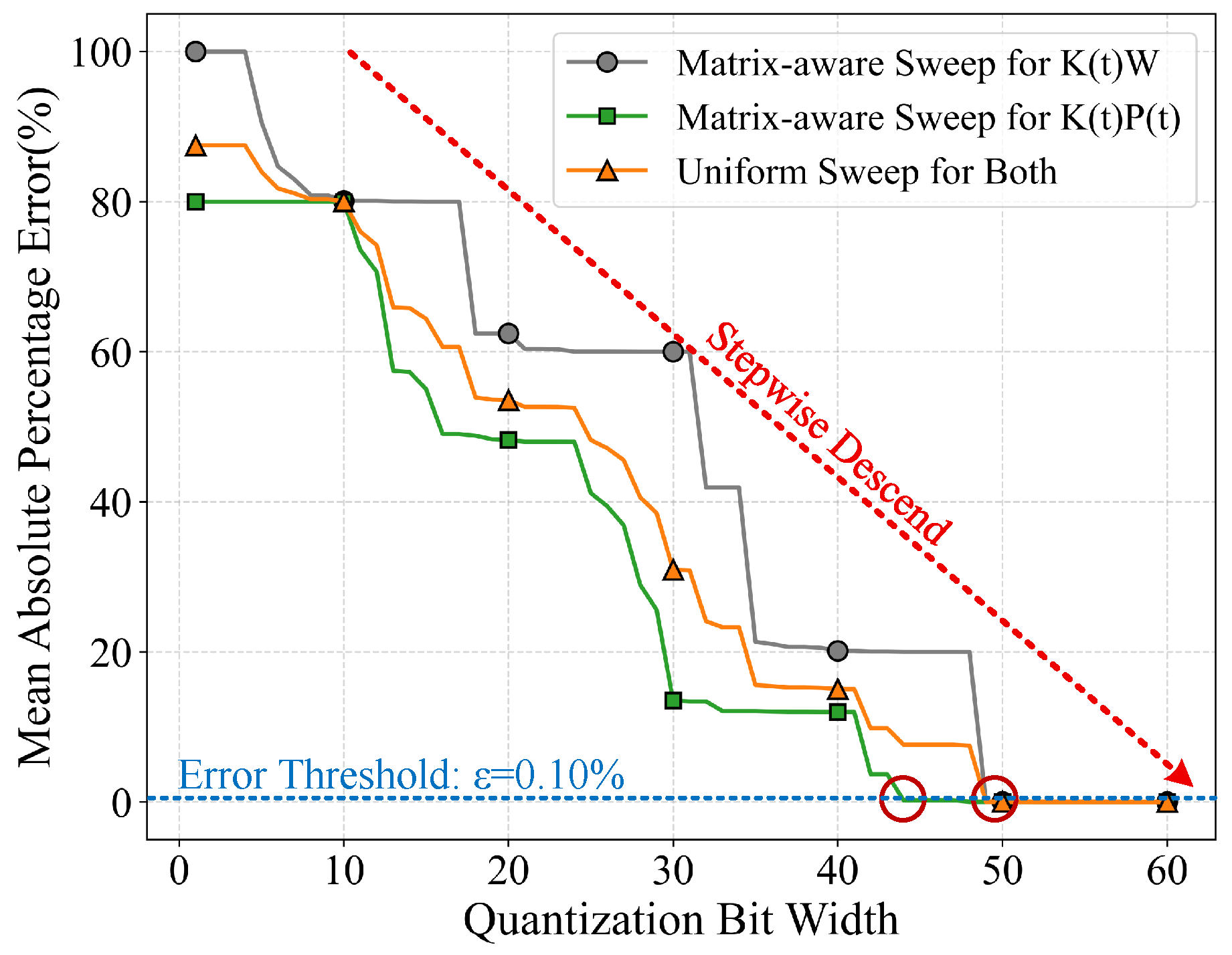
Our matrix-aware fixed-point quantization approach was evaluated using standard state-space coefficient matrices, specifically the K ( t ) W and K ( t ) P ( t ) matrices from Equation (6). The quantization test results demonstrate that the mean absolute percentage error (MAPE) exhibits a stepwise decrease as the quantization bit-width increases, eventually falling below the 0.10% error threshold at a certain critical point, beyond which further bit-width increases yield diminishing returns. As indicated by the red circular markers in Figure 16, these inflection points were identified and subsequently adopted as the optimal quantization bit-widths for storing the coefficient matrices in hardware memory, achieving an optimal balance between precision and resource efficiency.
The error threshold ϵ established in Section 4.2 is determined based on the MAPE range. During the discretization of state-space equations in power systems, matrix inversion operations are typically involved [10,17], which would introduce small numerical values. As illustrated in Figure 16, a high ϵ setting would yield smaller quantized bit-widths during the search process, causing these small values to be quantized to zero. The preservation of these small values is essential for ensuring the convergence of EMT computational results. To maintain their integrity, we strategically set the error threshold at the inflection point of the final step transition, corresponding to the 0.10% position on the characteristic curve.
Furthermore, compared with the uniform bit-width sweep approach, our matrix-aware quantization method enables fine-grained quantization width search for individual matrices. As shown in Figure 16, the uniform scheme requires all matrices to adopt the maximum bit-width, which would lead to higher DSP resource consumption. Our proposed K ( t ) W quantization promises more efficient resource utilization through adaptive bit-width allocation.

5.2.2. Verification for Computational Configuration

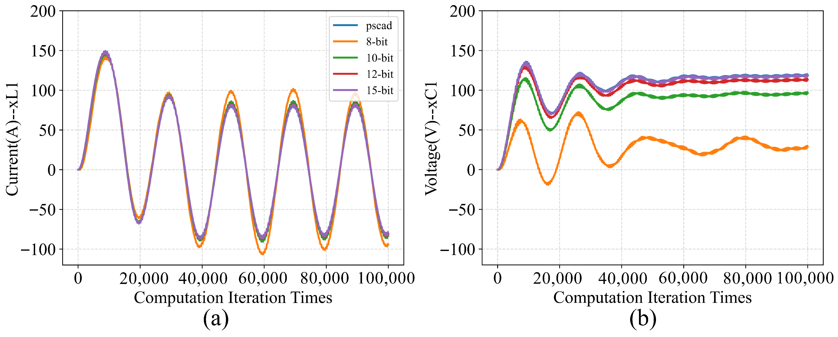
To validate the correctness of our previous computational configuration with the 15-bit and 18-bit fixed-point quantization bit width, we conducted a multi-precision comparative experiment using MATLAB R2022b, with the experimental results presented in Figure 17 and Figure 18. A converter module incorporates three inductors and two capacitors, resulting in a state vector x ( t ) = [ x L 1 ( t ) , x L 2 ( t ) , x L 3 ( t ) , x C 1 ( t ) , x C 2 ( t ) ] T . As demonstrated in Figure 17, computational analysis of state variables x C 1 and x L 2 reveals that quantization bit-widths below 14 bits induce matrix element truncation errors, resulting in transient distortion. Figure 18 quantifies the verification metrics through mean square error (MSE) and relative error (RE) comparisons between the computed state vectors and PSCAD reference solutions. The experimental data confirms that configurations with 15-bit width achieve MSE < 0.10 and RE < 0.20 % , meeting precision thresholds for power system computation.

5.2.3. Verification for Graph-Based Analysis

The converter design was deployed across CPU, GPU, and FPGA platforms, with runtime metrics measured both with and without WDP optimization, as shown in Table 2. The FPGA implementation achieved a remarkable 96.80% reduction in computation time, decreasing from 1.58 s to 0.05 s, which highlights its real-time processing capability. Similarly, the i9-14900K CPU showed a 13.90% improvement, reducing execution time from 22.77 s to 19.60 s. In contrast, the RTX 4090 GPU demonstrated a 41.90% speedup, lowering computation time from 121.07 s to 70.35 s, yet it still performed slower than the CPU. This result originates from the continuous coefficient matrix updates required for state-space equation computation. Although these matrices can be pre-cached in GPU memory, their selection depends on time-varying three-phase voltages, leading to significant interaction overhead. Furthermore, the strong iterative computational dependencies inherently restrict the GPU’s ability to fully utilize its fast matrix multiplication capabilities.
To validate our approach, we reimplemented the work of Xu et al. [17] and applied our WDP optimization, achieving substantial efficiency gains across all metrics. As shown in Table 3, the optimized design reduces DSP consumption per converter by 42.90% from 21 to 12 while improving latency by 25.40%. On the XCKU060 platform, we achieved an 18.50% reduction in LUT usage and a 37.60% decrease in FF consumption. The U55C platform shows similar improvements, with LUT resources decreasing by 8.70% from 1602 to 1463 and FF utilization dropping by 35.30% from 2671 to 1727. These quantitative results demonstrate our method’s consistent effectiveness in simultaneously enhancing both resource efficiency and computational performance across different FPGA architectures.
In fact, FPGA-based EMT simulator offers distinct advantages over GPU-accelerated approaches, particularly in latency-sensitive applications. Compared to GPUs, FPGAs provide deterministic nanosecond-level latency, making them ideal for high-switching-frequency power electronics, where real-time control loops demand strict timing guarantees.
The implementations on XCKU060 and U55C platforms respectively can support hardware-in-loop (HIL) connections. For the XCKU060-based implementation, it can be achieved through expanded DAC and PWM interfaces, direct connection to the HIL controllers (e.g., DSP-based controllers) [10]. The U55C-based CPU-FPGA architecture employs PCIe connectivity to transfer HIL carrier control signals while enabling bidirectional data exchange between FPGA computations and CPU processing.

5.3. Performance

In this section, we evaluate the hardware deployment performance of our computational architecture, assessing its physical reliability along with key metrics including computational resource utilization, precision, latency, and scalability.

5.3.1. Physical Reliability

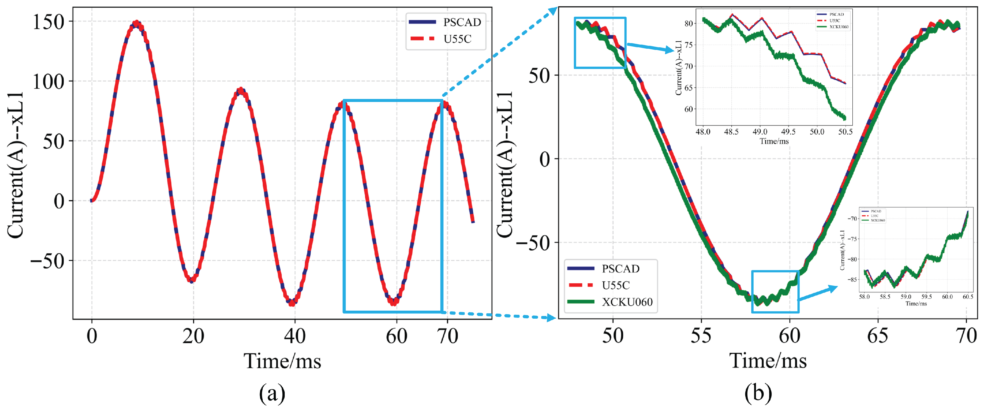
The experimental results in Figure 19 demonstrate excellent consistency between hardware implementations and PSCAD software benchmarks. Quantitative analysis shows the U55C-generated results as described in Figure 19a maintain a mean relative error of only 0.17% compared to PSCAD reference simulations. The analog test waveforms as depicted in Figure 19b show slight deviations primarily caused by hardware implementation limitations. These variations originate from measurement constraints, including 14-bit DAC quantization effects and inherent system noise, which collectively contribute to a 1.25% relative error in waveform fidelity.
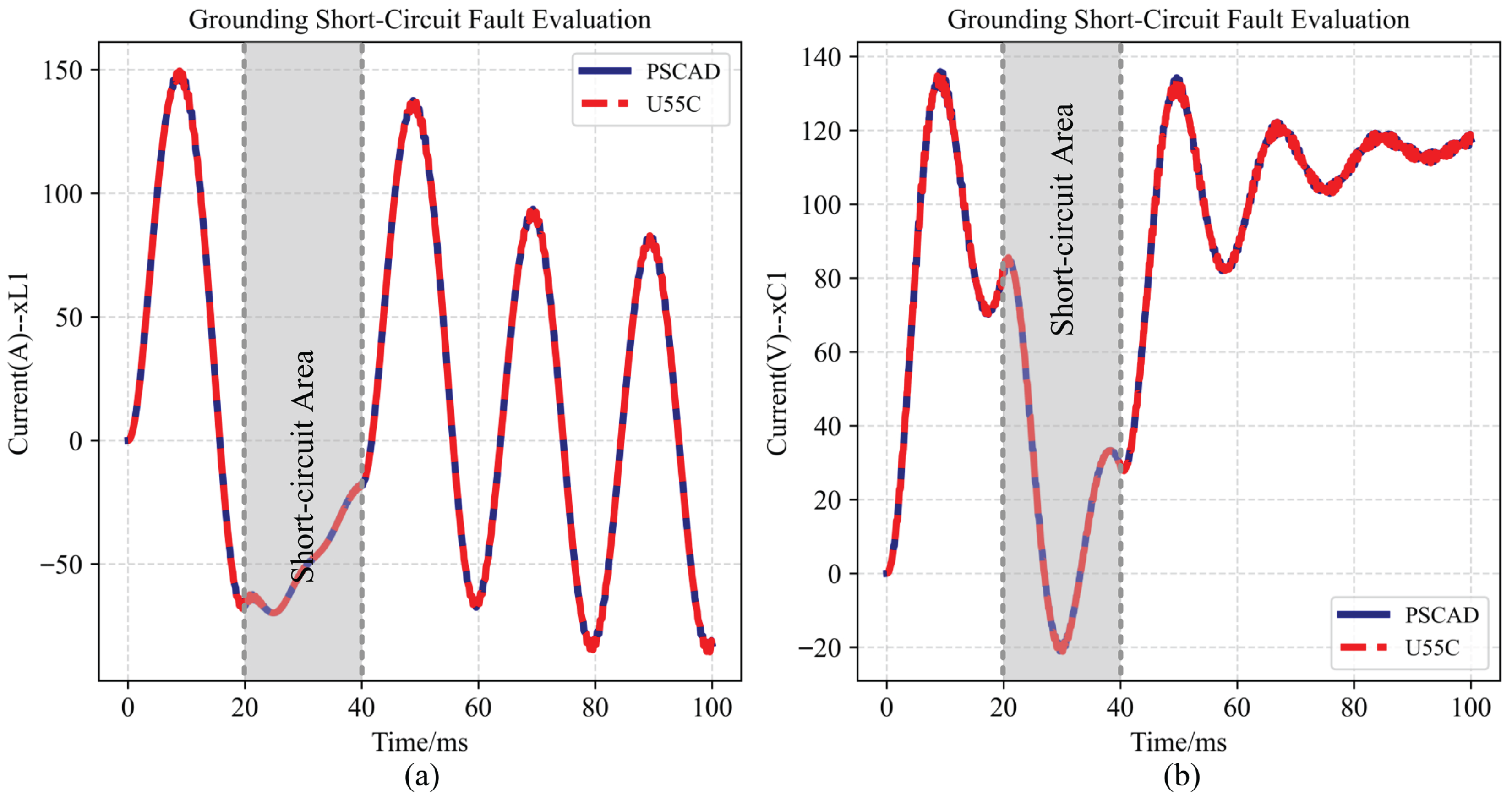
To evaluate adaptivity of our design, we have conducted a three-phase-to-ground short-circuit experiment [17]. As demonstrated in Figure 20, the grid occurs an three phase grounding fault between 20 ms and 40 ms with a duration of 20 ms. The comparative results between our FPGA implementation and software simulation in Figure 20a,b reveal the robustness of our hardware design and the effectiveness of the proposed matrix fixed-point quantization method under fault conditions, demonstrating their capability to simulate transient grid disturbances.

5.3.2. Versus Existing FPGA Accelerators for Single Converter

To assess the performance of our proposed design for single converter implementations, we perform a comprehensive comparison with state-of-the-art FPGA-based acceleration methods for voltage source converters. As summarized in Table 4, our approach exhibits substantial enhancements across multiple key metrics. When implemented on the same XCKU060 FPGA platform, our fully parallel converter architecture reduces DSP utilization by 51.43% compared to the state-of-the-art work by Xu et al. [17]. Furthermore, our design achieves superior computational accuracy, with a relative error of 0.17%, representing a 71.67% reduction compared to the previous best ADC-based solution with 0.60% error. The observed latency improvements are primarily attributed to an increased clock frequency. This is enabled by the elimination of redundant computation and an optimized processing sequence.

5.3.3. Versus Existing FPGA Accelerators for Multi-Converter Systems

To evaluate the scalability of the proposed design for multi-converter systems, we implemented a large-scale state-space equation solver with a 373 ns latency on the U55C FPGA-CPU heterogeneous platform. The U55C-based implementation leverages PCIe for data exchange with the CPU system, enabling large-scale expansion.
For comparative analysis, we implemented the same design on the XCKU060 FPGA, though this configuration was used solely for resource and scalability assessment. This limitation arises because the XCKU060 implementation relies on DAC outputs for signal generation. Given that each converter requires five state variables, a 14-bit DAC resolution necessitates 70 I/O pins per converter. With only 624 available I/O pins on the XCKU060, the platform can support a maximum of eight converters in parallel. Consequently, the XCKU060 implementation serves only as an auxiliary testbed, with all outputs multiplexed through a shared DAC rather than direct I/O connections. Figure 21 presents the scalability and resource consumption comparison on the XCKU060 platform. The results reveal that BRAM and DSP usage exhibit the most rapid growth among all computational resources. For the fully parallel implementation as shown in Figure 21a, DSP consumption increases disproportionately, reaching saturation before 500 switches. Beyond this threshold, further scaling requires replacing DSPs with LUTs, albeit at the cost of degraded timing performance. In contrast, the pipelined implementation as described in Figure 21b shows BRAM consumption surpassing DSP usage.
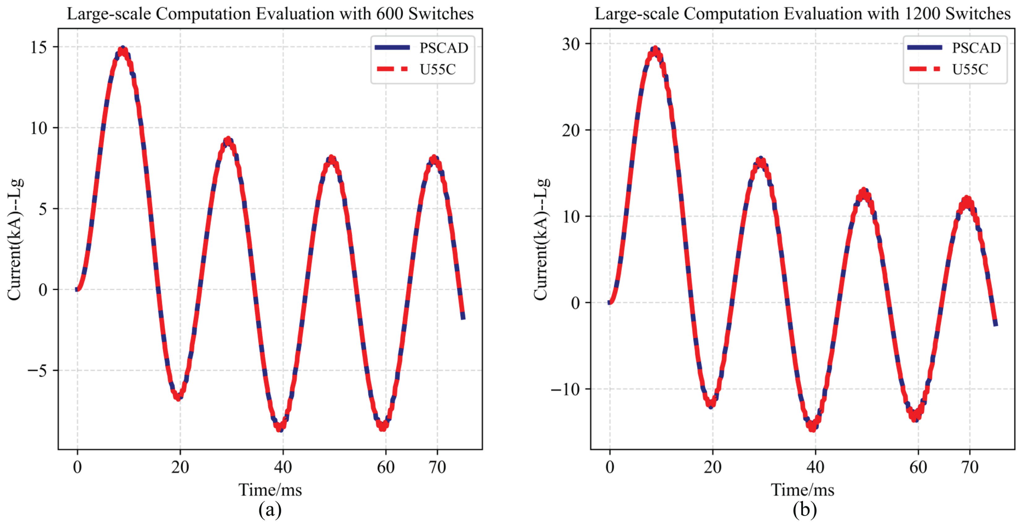
To comprehensively evaluate the relative error of our design under large-scale expansion, experimental validation was performed on multi-VSC systems at two representative scales including 600-switch and 1200-switch configurations. The corresponding three-phase current measurements at the grid interface following multi-VSC synchronization are illustrated in Figure 22. The relative error of the former is 0.08%, while that of the latter with 1200 switches is 0.12%.
Additionally, Table 5 details the deployment of the 373 ns pipelined design on the U55C FPGA. Our implementation achieves a 1200-switch scale while maintaining 373 ns latency. Resource usage trends align with those observed on the XCKU060, with BRAM demand growing most rapidly. Although LUT and FF consumption increases linearly, their growth rates remain significantly slower than those of BRAM and DSP.
To validate the topological adaptability of our approach, we implemented the trunk multi-converter system on a U55C FPGA platform. Unlike the radial multi-converter system, the trunk topology exhibits greater structural complexity and stronger matrix computation dependencies [17]. As presented in Table 6, our implementation achieves up to 330 switches. The proposed accelerator demonstrates optimal performance for radial multi-converter system, while maintaining applicability to other topologies such as trunk multi-converter systems through appropriate design adjustments.
To further evaluate the scalability of our design, we conducted a comprehensive survey of recent works targeting multi-converter systems and compiled the results in Table 7. We adopt the number of switches as the unified metric for system scale assessment in multi-converter systems, following the established practice in recent works by Zheng et al. [10] and Xu et al. [17]. As shown in Table 7, the settings for high accuracy and low latency account for most existing designs. In this table, we focus on the aspects of scalable design and computational capacity. As demonstrated in Table 7, our work achieves 1.54 × to 200.00 × scale increases for EMT solvers in multi-converter systems, compared to state-of-the-art approaches. Although most existing studies claim scalability, their experimental validations rely on traditional FPGA implementations with physical DAC outputs. We remark that such implementations may face inherent limitations due to I/O resource constraints. Our work represents a novel and practical realization of large-scale converter computation with inherent support for communication interconnection and expansion.

5.3.4. Bandwidth Evaluation

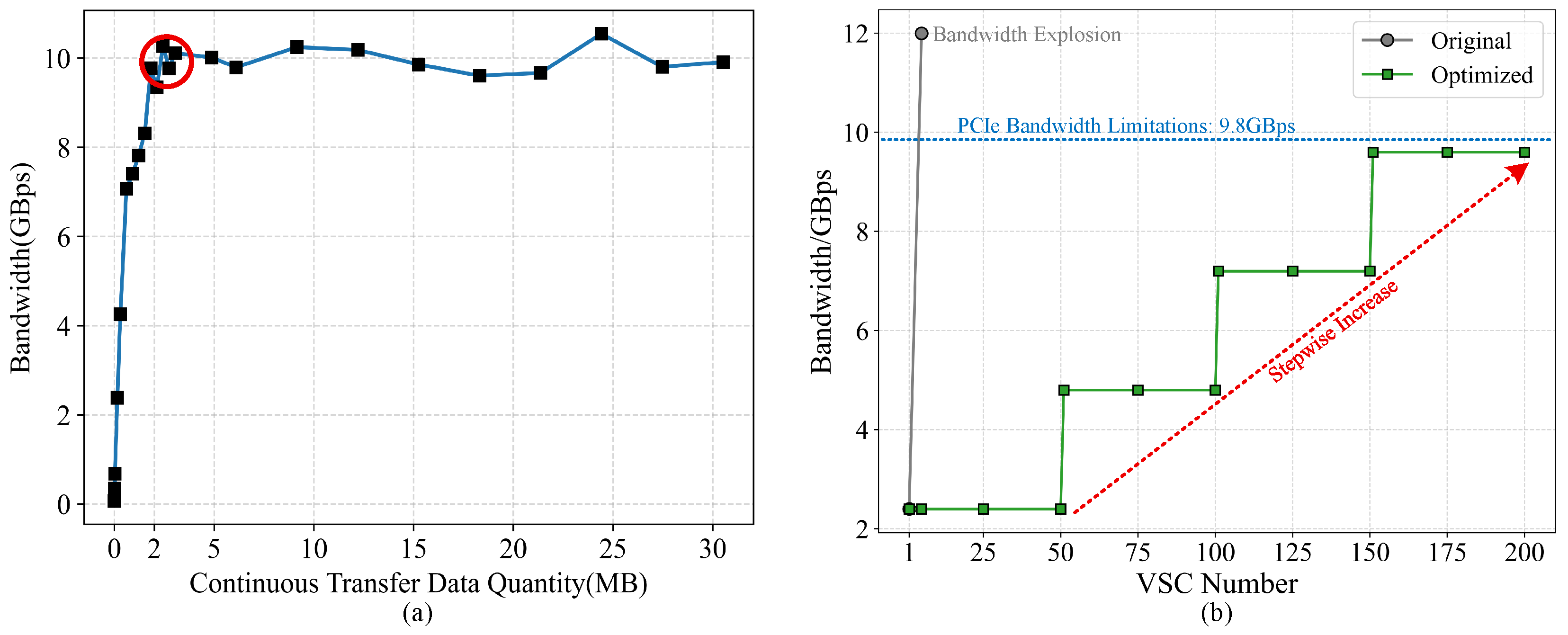
To comprehensively evaluate the bandwidth optimization effectiveness of our scalable architecture, we test the physical PCIe bandwidth between the U55C FPGA and host CPU, as shown in Figure 23a. For continuous data transfers exceeding 2 MB, our measurements indicate an effective PCIe Gen3x16 bandwidth of approximately 10 GBps for payload data transfer.
Based on this, we further present comparative analyses of bandwidth consumption versus VSC number for both unoptimized parallel computation and our proposed pipelined architecture with latency-insertion optimization in Figure 23b. The results demonstrate that the original parallel approach causes instantaneous bandwidth to surge dramatically, exceeding the available bandwidth with merely 5 VSCs. In contrast, our proposed pipelined architecture with latency-insertion method enables system scalability up to 200 VSCs with 1200 switches.
As evidenced in Figure 23b, the current performance bottleneck in large-scale EMT computation primarily stems from bandwidth limitations, although our proposed latency-insertion method achieves stepwise bandwidth enhancement. If this fundamental bandwidth constraint remain unresolved, further system scaling would face significant challenges. To overcome this bandwidth limitation, we suggest three approaches including optimizing data transfer protocols to reduce redundant data transfer [49], implementing multi-FPGA distributed computing architectures to avoid bandwidth limitations [50], and adopting compute-in-memory (CIM) paradigms to localize all matrix operations within memory arrays [51,52].

6. Conclusions

This article presents a large-scale state-space equation FPGA accelerator for EMT computation in multi-converter systems. To address scalability challenges, we introduce domain-specific components and a data-centric processing element (PE) array, effectively leveraging transfer intervals. For mapping the coefficient matrices of the equations and implementing matrix quantization, we propose a graph-based analysis method and a matrix-aware fixed-point quantization approach. Comparative experiments on i9-14900K, RTX4090, and U55C FPGA platforms demonstrate the effectiveness of our graph analysis and quantization methods. Performance and scalability evaluations of the FPGA accelerator highlight significant achievements in computational latency, resource efficiency, and accuracy while significantly enhancing scalability. We have realized a scalable interconnected architecture without being constrained by I/O resources. Experimental results demonstrate that our design achieves a computational scale of up to 1200 switches while maintaining 99.87% accuracy and 373 ns latency. Compared to state-of-the-art approaches, our work achieves an up-to 200.00 × scale increase for EMT solvers in multi-converter systems.

Author Contributions

Conceptualization, J.L. and M.X.; methodology, J.L. and M.X.; software, J.L.; validation, M.X.; formal analysis, J.L., M.X. and H.Y.; writing—original draft preparation, J.L.; writing—review and editing, J.L., Z.Q. and H.L.; visualization, J.L. and H.Y.; supervision, Z.Q., W.G., Y.T. and B.W.; project administration, W.G., Y.T., B.W. and H.L.; funding acquisition, H.L. All authors have read and agreed to the published version of the manuscript.

Funding

This work is supported in part by the National Natural Science Foundation of China under Grant 62304037, in part by the Natural Science Foundation of Jiangsu Province under Grant BK20230828, in part by the Jiangsu Provincial Scientific Research Center of Applied Mathematics under Grant BK20233002, in part by the Young Elite Scientists Sponsorship Program by CAST under Grant 2022QNRC001, in part by the Southeast University Interdisciplinary Research Program for Young Scholars under Grant 2024FGC1005, in part by the Fundamental Research Funds for the Central Universities under Grant 2242025K30008, and in part by the Start-up Research Fund of Southeast University under Grant RF1028623173.

Data Availability Statement

The original contributions presented in this study are included in the article. Further inquiries can be directed to the corresponding author.

Conflicts of Interest

The authors declare no conflicts of interest.

References

  1. Liu, D.; Zhang, X.; Tse, C.K. Effects of High Level of Penetration of Renewable Energy Sources on Cascading Failure of Modern Power Systems. IEEE J. Emerg. Sel. Top. Circuits Syst. 2022, 12, 98–106. [Google Scholar] [CrossRef]
  2. Wachter, J.; Gröll, L.; Hagenmeyer, V. Survey of Real-World Grid Incidents—Opportunities, Arising Challenges and Lessons Learned for the Future Converter Dominated Power System. IEEE Open J. Power Electron. 2024, 5, 50–69. [Google Scholar] [CrossRef]
  3. Xie, H.; Jiang, M.; Zhang, D.; Goh, H.H.; Ahmad, T.; Liu, H.; Liu, T.; Wang, S.; Wu, T. IntelliSense technology in the new power systems. Renew. Sustain. Energy Rev. 2023, 177, 113229. [Google Scholar] [CrossRef]
  4. Xu, M.; Gu, W.; Cao, Y.; Chen, S.; Zhang, F.; Liu, W. Low-Dimensional Equivalent Models and Multithreading-Based Parallel EMT Simulation Method for Multi-Converter Systems. IEEE Trans. Energy Convers. 2025, 40, 437–452. [Google Scholar] [CrossRef]
  5. Ge, H.; Liang, Y.; Lei, J.; Yuan, C.; Huang, Z. Neural ODE Model of Power Electronic Converters with Accelerated Computation and High Fidelity. IEEE Trans. Circuits Syst. I Regul. Pap. 2024, 71, 6363–6374. [Google Scholar] [CrossRef]
  6. Liu, Y.; Sun, K. Solving Power System Differential Algebraic Equations Using Differential Transformation. IEEE Trans. Power Syst. 2020, 35, 2289–2299. [Google Scholar] [CrossRef]
  7. Gourounas, D.; Hanindhito, B.; Fathi, A.; Trenev, D.; John, L.K.; Gerstlauer, A. FAWS: FPGA Acceleration of Large-Scale Wave Simulations. In Proceedings of the 2023 IEEE 34th International Conference on Application-specific Systems, Architectures and Processors (ASAP), Porto, Portugal, 19–21 July 2023; pp. 76–84. [Google Scholar] [CrossRef]
  8. Chen, Q. EI-NK: A Robust Exponential Integrator Method With Singularity Removal and Newton–Raphson Iterations for Transient Nonlinear Circuit Simulation. IEEE Trans.-Comput.-Aided Des. Integr. Circuits Syst. 2022, 41, 1693–1703. [Google Scholar] [CrossRef]
  9. Zhou, X.; Zhao, D.; Geng, Z.; Xu, L.; Yan, S. FPGA Implementation of Non-Commensurate Fractional-Order State-Space Models. IEEE Trans. Circuits Syst. I Regul. Pap. 2023, 70, 3639–3652. [Google Scholar] [CrossRef]
  10. Zheng, J.; Zeng, Y.; Zhao, Z.; Liu, W.; Xu, H.; Ji, S. A Semi-Implicit Parallel Leapfrog Solver with Half-Step Sampling Technique for FPGA-Based Real-Time HIL Simulation of Power Converters. IEEE Trans. Ind. Electron. 2024, 71, 2454–2464. [Google Scholar] [CrossRef]
  11. Xu, H.; Zheng, J.; Zeng, Y.; Liu, W.; Zhao, F.; Qu, C.; Zhao, Z. Topology-Aware Matrix Partitioning Method for FPGA Real-Time Simulation of Power Electronics Systems. IEEE Trans. Ind. Electron. 2024, 71, 7158–7168. [Google Scholar] [CrossRef]
  12. Ma, X.; Yang, C.; Zhang, X.P.; Xue, Y.; Li, J. Real-Time Simulation of Power System Electromagnetic Transients on FPGA Using Adaptive Mixed-Precision Calculations. IEEE Trans. Power Syst. 2023, 38, 3683–3693. [Google Scholar] [CrossRef]
  13. Mirzahosseini, R.; Iravani, R. Small Time-Step FPGA-Based Real-Time Simulation of Power Systems Including Multiple Converters. IEEE Trans. Power Deliv. 2019, 34, 2089–2099. [Google Scholar] [CrossRef]
  14. Yu, Z.; Zhao, Z.; Shi, B.; Zhu, Y.; Ju, J. An Automated Semi–symbolic State Equation Generation Method for Simulation of Power Electronic Systems. IEEE Trans. Power Electron. 2021, 36, 3946–3956. [Google Scholar] [CrossRef]
  15. Bhattacharya, S.; Grégoire, L.A.; Kallo, J.; Stevic, M.; Garg, M.; Willich, C. FPGA-based Real-Time Simulation for LLC Resonant Converter Prototyping. In Proceedings of the 2022 IEEE 13th International Symposium on Power Electronics for Distributed Generation Systems (PEDG), Kiel, Germany, 26–29 June 2022; pp. 1–6. [Google Scholar] [CrossRef]
  16. Paull, J.; Knickle, C.; Lofroth, N.; Wang, L.; Li, W. Adaptive-Grained Exponential Integrator Algorithm for Efficient Simulation of Power Converter Systems. IEEE Trans. Power Deliv. 2025, 40, 1114–1128. [Google Scholar] [CrossRef]
  17. Xu, M.; Liu, J.; Gu, W.; Cao, Y.; Chen, S.; Zhang, F.; Liu, W.; Tang, Y.; Li, H. A Real-Time Simulation Model with Constant Admittance Matrix for Multiple Grid-Connected Converters System. IEEE Trans. Power Electron. 2025, 40, 15080–15092. [Google Scholar] [CrossRef]
  18. Fan, X.; Liu, S.; Jiang, C.; An, S.; Liu, J. VSC Converter Real-time Simulation Modeling Method Research and FPGA Implementation. In Proceedings of the 2023 Panda Forum on Power and Energy (PandaFPE), Chengdu, China, 27–30 April 2023; pp. 466–471. [Google Scholar] [CrossRef]
  19. Xu, M.; Gu, W.; Cao, Y.; Chen, S.; Zhang, F.; Liu, W. A State Variables Elimination-Based EMTP-Type Constant Admittance Equivalent Modeling Method for Power Electronic Converters. IEEE Trans. Power Deliv. 2025, 40, 1100–1113. [Google Scholar] [CrossRef]
  20. Sun, Z.; Wang, G.; Li, Z.; Guo, X.; Zhang, Y. Real-Time Simulation Method for Power Electronic Converters with Low Resource Consumption. IEEE Trans. Power Electron. 2025, 40, 4695–4700. [Google Scholar] [CrossRef]
  21. Wang, K.; Xu, J.; Li, G.; Tai, N.; Tong, A.; Hou, J. A Generalized Associated Discrete Circuit Model of Power Converters in Real-Time Simulation. IEEE Trans. Power Electron. 2019, 34, 2220–2233. [Google Scholar] [CrossRef]
  22. Ould-Bachir, T.; Blanchette, H.F.; Al-Haddad, K. A Network Tearing Technique for FPGA-Based Real-Time Simulation of Power Converters. IEEE Trans. Ind. Electron. 2015, 62, 3409–3418. [Google Scholar] [CrossRef]
  23. Górecki, P. Electrothermal Averaged Model of a Diode–IGBT Switch for a Fast Analysis of DC–DC Converters. IEEE Trans. Power Electron. 2022, 37, 13003–13013. [Google Scholar] [CrossRef]
  24. Tse, K.; Hung, H.H.; Hui, S. Quadratic state-space modeling technique for analysis and simulation of power electronic converters. IEEE Trans. Power Electron. 1999, 14, 1086–1100. [Google Scholar] [CrossRef]
  25. Milton, M.; Benigni, A.; Bakos, J. System-Level, FPGA-Based, Real-Time Simulation of Ship Power Systems. IEEE Trans. Energy Convers. 2017, 32, 737–747. [Google Scholar] [CrossRef]
  26. Liu, C.; Ma, R.; Bai, H.; Gechter, F.; Gao, F. A new approach for FPGA-based real-time simulation of power electronic system with no simulation latency in subsystem partitioning. Int. J. Electr. Power Energy Syst. 2018, 99, 650–658. [Google Scholar] [CrossRef]
  27. Xu, J.; Wang, K.; Wu, P.; Li, G. FPGA-Based Sub-Microsecond-Level Real-Time Simulation for Microgrids with a Network-Decoupled Algorithm. IEEE Trans. Power Deliv. 2020, 35, 987–998. [Google Scholar] [CrossRef]
  28. Silva, S.N.; Goldbarg, M.A.S.d.S.; Silva, L.M.D.d.; Fernandes, M.A.C. Real-Time Simulator for Dynamic Systems on FPGA. Electronics 2024, 13, 4056. [Google Scholar] [CrossRef]
  29. Wang, Q.; Wang, C.; Pan, X.; Liang, L. Fixed-admittance Switch Model Correction Algorithm and Real-time Simulation Architecture of Power Electronics Based on Field Programmable Gate Array. Autom. Electr. Power Syst. 2024, 48, 150–159. [Google Scholar] [CrossRef]
  30. Wang, C.; Wang, Q.; Weng, H.; Pan, X. A Modified Algorithm for the L/C-based Switch Model of Power Converters in Real-Time Simulation Based on FPGA. IEEE Trans. Ind. Appl. 2024, 60, 7030–7037. [Google Scholar] [CrossRef]
  31. Guo, X.; Yuan, J.; You, X.; Zhang, Z. Research on FPGA optimization approach of power electronics real-time simulation modeling. Electr. Mach. Control 2020, 24, 12–19. [Google Scholar] [CrossRef]
  32. Zhao, F.; Du, J.; Deng, Y.; Zheng, J.; Zeng, Y.; Qu, C. An Adaptive Word-Length Selection Method to Optimize Hardware Resources for FPGA-Based Real-Time Simulation of Power Converters. IEEE Access 2023, 11, 122980–122990. [Google Scholar] [CrossRef]
  33. Ke, L.; Wei, G.; Wei, L.; Yan, C.; Guannan, L.; Dehu, Z. Real-time Parallel Multi-rate Electromagnetic Transient Simulation Method for Converters Based on Field Programmable Gate Array. Autom. Electr. Power Syst. 2022, 46, 151–158. [Google Scholar] [CrossRef]
  34. Yang, Y.; Xu, J.; Wang, K.; Wu, P.; Li, Z.; Li, G. A Delay-Free Decoupling Method for FPGA-Based Real-Time Simulation of Power Electronic Systems. IEEE J. Emerg. Sel. Top. Ind. Electron. 2025, 6, 391–402. [Google Scholar] [CrossRef]
  35. Xu, J.; Wu, P.; Li, Z.; Wang, K.; Li, G.; Han, B. Switching-Period-Synchronization-Based Real-Time Simulation Method Suitable for Power Converters with High Switching Frequency. IEEE Trans. Ind. Electron. 2025, 72, 10215–10226. [Google Scholar] [CrossRef]
  36. Batina, L.; Bhasin, S.; Jap, D.; Picek, S. CSI NN: Reverse Engineering of Neural Network Architectures Through Electromagnetic Side Channel. In Proceedings of the 28th USENIX Security Symposium (USENIX Security 19), Santa Clara, CA, USA, 14–16 August 2019; pp. 515–532. [Google Scholar]
  37. Ni, T.; Zhang, X.; Zhao, Q. Recovering Fingerprints from In-Display Fingerprint Sensors via Electromagnetic Side Channel. In Proceedings of the 2023 ACM SIGSAC Conference on Computer and Communications Security, CCS ’23, Copenhagen, Denmark, 26–30 November 2023; pp. 253–267. [Google Scholar] [CrossRef]
  38. Milton, M.; Benigni, A.; Monti, A. Real-Time Multi-FPGA Simulation of Energy Conversion Systems. IEEE Trans. Energy Convers. 2019, 34, 2198–2208. [Google Scholar] [CrossRef]
  39. Xia, S.; Xu, J.; Guo, L.; Li, S.; Guo, H. Real-Time Modeling Method for Large-Scale Photovoltaic Power Stations Using Nested Fast and Simultaneous Solution. IEEE Trans. Ind. Electron. 2025, 72, 2679–2689. [Google Scholar] [CrossRef]
  40. Yumoto, J.; Misumi, T. Equivalence of lattice operators and graph matrices. Prog. Theor. Exp. Phys. 2024, 2024, 023B03. [Google Scholar] [CrossRef]
  41. Kumar, M.; Gupta, R. Stability and Sensitivity Analysis of Uniformly Sampled DC-DC Converter with Circuit Parasitics. IEEE Trans. Circuits Syst. I Regul. Pap. 2016, 63, 2086–2097. [Google Scholar] [CrossRef]
  42. Dufour, C.; Mahseredjian, J.; Bélanger, J. A Combined State-Space Nodal Method for the Simulation of Power System Transients. IEEE Trans. Power Deliv. 2011, 26, 928–935. [Google Scholar] [CrossRef]
  43. Yu, S.; Zhang, S.; Han, Y.; Wei, Y.; Zou, S. A Pulse-Source-Pair-Based AC/DC Interactive Simulation Approach for Multiple-VSC Grids. IEEE Trans. Power Deliv. 2021, 36, 508–521. [Google Scholar] [CrossRef]
  44. Chalangar, H.; Ould-Bachir, T.; Sheshyekani, K.; Mahseredjian, J. Methods for the Accurate Real-Time Simulation of High-Frequency Power Converters. IEEE Trans. Ind. Electron. 2022, 69, 9613–9623. [Google Scholar] [CrossRef]
  45. Zeng, Y.; Zheng, J.; Zhao, Z.; Liu, W.; Ji, S.; Li, H. Real-Time Digital Mapped Method for Sensorless Multitimescale Operation Condition Monitoring of Power Electronics Systems. IEEE Trans. Ind. Electron. 2024, 71, 3628–3638. [Google Scholar] [CrossRef]
  46. Gao, C.; Fei, S.; Ma, Y.; Xu, J.; Wang, K.; Li, G. Multi-Domain-Mapping-Based Impedance Calculation Method for Oscillatory Stability Analysis of VSC-Based Power System. IEEE Trans. Power Syst. 2025, 40, 780–792. [Google Scholar] [CrossRef]
  47. OPAL-RT. Redefining Speed, Power and Accuracy of Real-Time FPGA Simulations. 2024. Available online: https://www.opal-rt.com/solver-ehs (accessed on 12 December 2024).
  48. Benigni, A.; Strasser, T.; De Carne, G.; Liserre, M.; Cupelli, M.; Monti, A. Real-Time Simulation-Based Testing of Modern Energy Systems: A Review and Discussion. IEEE Ind. Electron. Mag. 2020, 14, 28–39. [Google Scholar] [CrossRef]
  49. Liu, J.; Wang, B.; Tang, Y.; Li, H. Fine-grained data integration for high throughput and bandwidth-efficient computation on FPGAs. Integration 2025, 106, 102563. [Google Scholar] [CrossRef]
  50. Yang, H.; Liu, J.; Xu, M.; Gu, W.; Tang, Y.; Li, H. Scalable and Real-Time Power System Simulation Based on Heterogeneous CPU-FPGA Co-operation. In Proceedings of the 2025 IEEE International Symposium on Circuits and Systems (ISCAS), London, UK, 25–28 May 2025; pp. 1–5. [Google Scholar] [CrossRef]
  51. Vignali, R.; Zurla, R.; Pasotti, M.; Rolandi, P.L.; Singh, A.; Gallo, M.L.; Sebastian, A.; Jang, T.; Antolini, A.; Scarselli, E.F.; et al. Designing Circuits for AiMC Based on Non-Volatile Memories: A Tutorial Brief on Trade-Off and Strategies for ADCs and DACs Co-Design. IEEE Trans. Circuits Syst. II Express Briefs 2024, 71, 1650–1655. [Google Scholar] [CrossRef]
  52. Kneip, A.; Lefebvre, M.; Verecken, J.; Bol, D. IMPACT: A 1-to-4b 813-TOPS/W 22-nm FD-SOI Compute-in-Memory CNN Accelerator Featuring a 4.2-POPS/W 146-TOPS/mm2 CIM-SRAM with Multi-Bit Analog Batch-Normalization. IEEE J. Solid-State Circuits 2023, 58, 1871–1884. [Google Scholar] [CrossRef]
Figure 1. The overview of FPGA-accelerated EMT computation. This article focuses on accelerating large-scale EMT computation through systematic exploration of scalable hardware architecture and design optimization methods, particularly targeting state-space equations derived from power grid EMT models under power outage scenarios.
Electronics 14 03966 g001
Figure 2. The overview of proposed hardware architecture. Our design can support traditional FPGAs with hardware in loop and advanced FPGAs with accelerator card framework.
Electronics 14 03966 g002
Figure 3. Customized components for EMT computation of multi-converter systems. (a) Carrier wave generator. (b) Source wave generator. (c) Switch Signals generator.
Electronics 14 03966 g003
Figure 4. The workflow of memory mapping and matrix multiplication.
Electronics 14 03966 g004
Figure 5. Example of memory mapping distribution and the computation workflow with different mode, where ADDR represent the start address in BRAM, SW denotes the 3-bit switch signal, and data[3:0] is responsible for stored column vector of coefficient matrices in the memory. The x ( t ) denotes the state vector at the t-th clock.
Electronics 14 03966 g005
Figure 6. Example of matrix multiplication kernel (MMK) module when m = 4 and x ( t ) = [ x 1 ( t ) , x 2 ( t ) , x 3 ( t ) , x 4 ( t ) ] T .
Electronics 14 03966 g006
Figure 7. Example of different transfers, where x c i ( t ) represents the state vector of ith converter. (a) Direct transfer with high instantaneous bandwidth has large waste. (b) Latency-insertion transfer with low instantaneous bandwidth spreads the instantaneous bandwidth evenly across each clock.
Electronics 14 03966 g007
Figure 8. Example of final bandwidth optimizations with N m a x = 10 , where x c i ( t ) represents the state vector of i-th converter, Δ t = 4 .
Electronics 14 03966 g008
Figure 9. The workflow of latency insertion including idle state for writing registers, configuration state for writing latency values to each PE and computation state. During PE computation, if the latency control module monitors count value more than L i , then it enables next calculation. Otherwise, the ready signal maintains low to stop all the calculation.
Electronics 14 03966 g009
Figure 10. Design of processing element (PE) module.
Electronics 14 03966 g010
Figure 11. Topologies of graph (a), weighted graph (b), digraph (c), and (d) weighted diagraph with priority (WDP).
Electronics 14 03966 g011
Figure 12. The logic equivalence rules based on the fundamental operation laws of matrices. (a) The commutative law of addition. (b) The associative law of addition. (c) The associative law of multiplication. (d) The distributive law of multiplication. (e) The elimination of the identity matrix. (f) The introduction of the identity matrix.
Electronics 14 03966 g012
Figure 13. The setup and optimization of a WDP for Equation (6), where each vertex is assigned an exemplary weight. (a) Build expression digraph. (b) Append the priority and allocate weight for each edge to establish the WDP. (c) Adjust the WDP by following logic equivalence. (d) Optimized WDP.
Electronics 14 03966 g013
Figure 14. The instance of mapping from a WDP to the PE module.
Electronics 14 03966 g014
Figure 15. Real machine operation for real-time computation based on FPGAs. (a) FPGA-CPU heterogeneous system equipped with AMD Alveo U55C accelerator cards is used to deploy large-scale EMT computation. (b) U55C FPGAs are connected to CPU server by PCIe interface. (c) The high-performance XCKU060-implemented computation system with 125 MHz DAC.
Electronics 14 03966 g015
Figure 16. Proposed matrix-aware fixed-point quantization bit width search method and uniform bit-width sweep method for coefficient matrices.
Electronics 14 03966 g016
Figure 17. Quantization verification for state variables ( x L 1 , x L 2 , x L 3 , x C 1 , x C 2 ) by MATLAB with various quantization widths. (a) The transient response of the state x L 1 . (b) The transient response of the state x C 1 .
Electronics 14 03966 g017
Figure 18. Quantization error for state variables ( x L 1 , x L 2 , x L 3 , x C 1 , x C 2 ) by MATLAB with various quantization widths. (a) The relationship between the mean squared error (MSE) and the quantization bit width. (b) The relationship between the relative error (RE) and the quantization bit width.
Electronics 14 03966 g018
Figure 19. Waveform results of real-time power system computation. (a) A-phase current of the VSC. (b) Enlargement of A-phase current waveform near 60 ms in (a), including PSCAD results, U55C transferring data by PCIe, and KU060 outputting physical waveform by 14-bit DAC.
Electronics 14 03966 g019
Figure 20. Grounding short-circuit fault evaluation. (a) The transient response of the state x L 1 . (b) The transient response of the state x C 1 .
Electronics 14 03966 g020
Figure 21. Relationship between resource consumption and computation scale. (a) FPGA-accelerated implementation obtains 53 ns ultra low latency and maintains 95 converters with 570 switches. (b) FPGA-accelerated implementation obtains 373 ns latency and maintains 150 converters with 900 switches.
Electronics 14 03966 g021
Figure 22. Evaluation of the relative errors for different switch scales. (a) Multi-converter system testing with 600 switches scale. (b) Multi-converter system testing with 1200 switches scale.
Electronics 14 03966 g022
Figure 23. Bandwidth limitations. (a) The relationship between PCIe bandwidth and data transfer volume in U55C. (b) The relationship between bandwidth and the number of VSCs.
Electronics 14 03966 g023
Table 1. Key variables for the proposed design (parameters listed in this table are collected directly by Xu et al.’s model [17]).
SymbolDescriptionSymbolDescription
G, G 0 , G 1 , etc.Topological graph ϵ Global error threshold 0.10 %
V, V 0 , V 1 , etc.Vertices set ξ Element-wise tolerance
E, E 0 , E 1 , etc.Edges set x L 1 ( t ) , etc.Inductance state variables
x ˙ ( t ) , x ( t ) State matrices x C 1 ( t ) , etc.Capacitance state variables
u ( t ) Input matrix R o n Switches on-resistance 0.005 Ω
I Identity matrix R o f f Switches off-resistance  10 6 Ω
A , B , etc.Matrices R l o a d Load resistance  20 Ω
Δ t Time step C 1 , C 2 Capacitance    3 × 10 3 F
G sub Sub-graphs set L 1 , L 2 , L 3 Inductance    8 × 10 3 H
g 1 , g 2 , etc.Sub-graph of G u a , u b , u c Three-phase voltage with 400 V magnitude
R F Receptive fields T r m s Maximum amplitude voltage 326 V
Q ( · ) Quantization operator R a , R b , R c Source resistor  0.5 Ω
Q min Smallest quantization width R g Line load resistance  0.5 Ω
Γ MAPE quantization error L g Line load inductance  8 × 10 3 H
Table 2. Comparison of runtime for various platforms.
PlatformFrequencyTime 1Time (with WDP) 1
U55C-FPGA150.00 MHz1.58 s0.05 s
EPYC-95543.76 GHz38.77 s33.32 s
i9-14900K6.00 GHz22.77 s19.60 s
i9-14900K + RTX40906.00 GHz121.07 s70.35 s
1 adopts 1000 ns time step and one million computation times.
Table 3. Comparison of resource utilization and latency.
Without WDPWith WDP
PlatformXCKU060XCU55CXCKU060XCU55C
LUTs1316160210731463
FFs1653267110321727
BRAMs35.535.535.535.5
DSPs21211212
Latency (ns)500500373373
Table 4. Comparisons of FPGA resource utilization and latency for single converter.
BenchmarkG-ADC [21]SNP [13]ADC [31]EP-ON [33]Zhao et al. [32]IEC [29]IEM [30]Xu et al. [17]OursOurs
Year2018201920202022202320242024202520252025
PlatformXC7K410TXC7VX485TXC7K325TXCKU060XC7VX485TXC7K325TXC7K325TXCKU060XCKU060XCU55
FrequencyNA175 MHzNA142.8 MHzNA50 MHz100 MHz100 MHz150 MHz150 MHz
LUTs50,734134,11013,43959,70216,98824,45623,731259315992102
FFs53,350129,73411,69979,60316,02415,89615,753205213282020
BRAMs91.0206.0NA129.5NA31.531.035.535.535.5
DSPs2113253371490468127128703435
Latency (ns)475800100455100500500805353
Related Errors (%)>5.00>5.000.601.511.00NANA0.860.170.17
Table 5. Resource consumption with 373 ns latency for radial topology on U55C FPGA.
Converters11020406080100120140160180200
Switches66012024036048060072084096010801200
LUTs1406828914,81328,88343,08757,08871,16285,19299,365113,432127,405141,467
FFs1737976118,73136,67154,61872,55690,499108,440126,382144,320162,264180,204
BRAMs35.594159289419549679809939106911991329
DSPs12120240480720960120014401680192021602400
Table 6. Resource consumption of proposed accelerator for trunk topology on U55C FPGA.
Converters510152025303540455055
Switches306090120150180210240270300330
LUTs32,25364,69697,578129,848161,430195,259227,809261,073293,339326,163376,949
FFs25,12249,75374,38198,942123,535148,227172,856197,500222,060246,699271,346
BRAMs142637.5496172.58496107.5119131
DSPs8281653247833034128495357786603742882539002
Table 7. Reported EMT solver for converter systems.
Existing SolversWork YearHigh Accuracy 4Low Latency 5Scalable DesignComputation Switches 6
SSN [42]2010--
L/C-ADC [21] 1,220186
G-ADC [21] 1,220186
SNP [13] 1,22019-36
LB-LMC [38] 1,2201938
ADC [31] 1,220206
EMT [43]202060
DMM [44] 1,220218
EP-ON [33] 1,220226
SPL [10] 1,22023120
RTDM [45] 1,220238
TA-MP [11] 1,22023224
IEC [29] 1,22024-6
IEM [30] 1,22024-6
MDM [46]2024-120
eHS [47] 1,32024-128
Xu et al. [17] 1,22025780
Ours 1,320251200
1 represents FPGA-accelerated implementations; 2 represents physical scaling through DAC output limited by I/O resources on FPGAs; 3 stands for FPGA-CPU heterogeneous scalability without limitations from I/O resources; 4 high accuracy represents related errors < 1.00 % in EMT computation [17]; 5 low latency means that the computation small time-step is ≤500 ns [48]; 6 computation switches represent the largest size of EMT computation [10,17].
Disclaimer/Publisher’s Note: The statements, opinions and data contained in all publications are solely those of the individual author(s) and contributor(s) and not of MDPI and/or the editor(s). MDPI and/or the editor(s) disclaim responsibility for any injury to people or property resulting from any ideas, methods, instructions or products referred to in the content.