Abstract
This work presents a low-power photoplethysmography (PPG) readout integrated circuit (IC) that achieves a wide dynamic range (DR) through the direct integration of a voltage-controlled oscillator (VCO)-based quantizer into the photodiode driver. Conventional PPG readout circuits rely on either transimpedance amplifier (TIA) or light-to-digital converter (LDC) topologies, both of which require auxiliary DC suppression loops. These additional loops not only raise power consumption but also limit the achievable DR. The proposed design eliminates the need for such circuits by embedding a linear regulator with a mirroring scale calibrator and a time-domain quantizer. The quantizer provides first-order noise shaping, enabling accurate extraction of the AC PPG signal while the regulator directly handles the large DC current component. Post-layout simulations show that the proposed readout achieves a signal-to-noise-and-distortion ratio (SNDR) of 40.0 dB at 10 µA DC current while consuming only 0.80 µW from a 2.5 V supply. The circuit demonstrates excellent stability across process–voltage–temperature (PVT) corners and maintains high accuracy over a wide DC current range. These features, combined with a compact silicon area of 0.725 mm2 using TSMC 250 nm bipolar–CMOS–DMOS (BCD) process, make the proposed IC an attractive candidate for next-generation wearable and biomedical sensing platforms.
1. Introduction
Photoplethysmography (PPG) is one of the most widely adopted non-invasive techniques for monitoring physiological conditions such as heart rate, oxygen saturation, and vascular health. The technique relies on illuminating tissue with a light source and measuring the intensity of the reflected or transmitted light using a photodiode. Variations in the optical signal correspond to blood volume changes and can be digitized for clinical or wearable health applications. Owing to its simplicity and low cost, PPG has become central to consumer health devices, ranging from smartwatches to ambulatory monitoring systems [1,2,3,4,5,6,7,8].
Despite its advantages, the design of efficient PPG readout electronics remains challenging. A conventional solution is the transimpedance amplifier (TIA), which converts photodiode current to voltage before digitization. Although TIAs achieve high linearity, they suffer from large DC offsets and require additional suppression loops, which consume power and degrade efficiency. Several works have attempted to mitigate these drawbacks through feedback techniques, gain-boosted architectures, or digitally assisted calibration [9,10,11,12,13]. Another approach is the light-to-digital converter (LDC), which integrates the photodiode current directly and employs incremental conversion schemes. LDCs extend the DR compared to TIAs, but they too depend on auxiliary DC rejection paths and often require complex calibration to maintain accuracy [14,15,16,17,18]. As summarized in prior studies, these conventional schemes result in unnecessary power overhead and architectural inefficiencies, especially in portable applications where battery life is critical.
To overcome these limitations, time-based signal processing has recently emerged as a compelling alternative. By embedding the quantization process directly into the current regulation path of the photodiode driver, the need for explicit DC suppression is removed. Frequency-to-digital conversion (FDC) techniques offer inherent first-order noise shaping, in which quantization noise is suppressed in the signal band and shifted toward higher frequencies, allowing precise recovery of small AC components in the presence of large DC currents. VCO-based quantizers in particular provide compact implementation and high energy efficiency, making them attractive for biomedical readout ICs [19,20,21,22,23].
In this work, we propose a low-power PPG readout IC that integrates a VCO-based quantizer into the sensor driver’s linear regulator. The design introduces a mirroring scale calibrator that stabilizes oscillation frequency under process and temperature variations. Extensive simulations, including PVT corners and DC current sweeps, confirm that the proposed readout achieves high SNDR, robust transient behavior, and excellent load regulation while consuming less than 1 µW. Compared with prior art, the circuit demonstrates a significantly improved figure-of-merit (FoM), validating its suitability for wearable and biomedical sensing systems.
2. Prior State-of-the-Art Designs
The design of PPG readout circuits has evolved over the past two decades, with two major families dominating the literature: transimpedance amplifier (TIA)-based readouts and light-to-digital converter (LDC)-based readouts. Both approaches provide workable solutions but share fundamental inefficiencies, particularly in handling the large DC component of photodiode current. In this section, we review representative circuits from each family and highlight their limitations.
2.1. TIA-Based Readout Circuits
The TIA remains the most classical solution for PPG sensing, as shown in Figure 1. By converting the photodiode current directly into voltage, followed by analog-to-digital conversion, TIAs offer excellent linearity and compatibility with conventional mixed-signal systems. However, in practice the photodiode generates a large DC offset current, sometimes exceeding the signal of interest by several orders of magnitude. To accommodate this, TIAs are typically augmented with DC suppression loops, such as digitally controlled feedback, automatic gain control, or baseline wander correction [9,10,11,12,13].
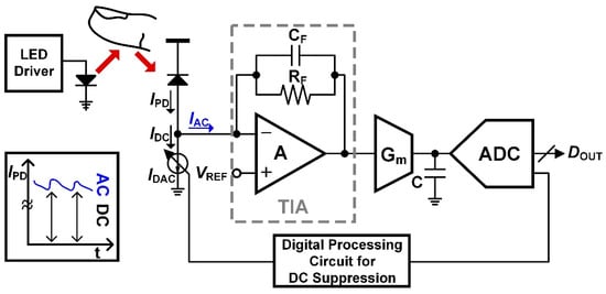
Figure 1.
Generalized architecture of a TIA-based PPG readout circuit. The photodiode current is converted into a voltage through a transimpedance amplifier, followed by an ADC stage. A DC suppression loop is included to mitigate the large offset current but introduces additional power consumption and circuit complexity.
While these techniques improve dynamic range, they introduce significant overhead. First, the suppression loop consumes additional current, conflicting with the low-power requirements of wearable systems. Second, the ADC following the TIA must support a wide input range, which reduces its effective resolution for the small AC component of the PPG waveform. Finally, the inclusion of large passive components (feedback resistors or capacitors) leads to increased area and design complexity.
Figure 1 illustrates the generalized architecture of a TIA-based PPG readout. The feedback network regulates the transimpedance gain while the suppression loop cancels part of the DC current. Nevertheless, the residual offset and power inefficiency remain problematic for continuous monitoring in battery-operated platforms.
2.2. LDC-Based Readout Circuits
To address the inefficiency of current-to-voltage conversion, researchers proposed direct light-to-digital conversion (LDC), as depicted in Figure 2. In this architecture, the photodiode current is integrated onto a capacitor, and the accumulated charge is digitized by an incremental converter [14,15,16,17,18]. This method inherently supports wider dynamic range compared to TIA-based designs, since it processes current in the charge domain rather than voltage domain.
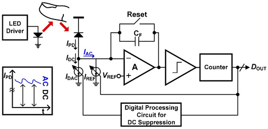
Figure 2.
Generalized architecture of an LDC-based PPG readout circuit. The photodiode current is directly integrated and digitized by an incremental converter. Although this approach improves dynamic range, it still requires a DC suppression loop and involves calibration complexity, reducing overall efficiency.
Despite these advantages, LDCs are not free from limitations. Similarly to TIAs, a separate DC suppression loop is still required, as the photodiode’s DC current must be rejected to avoid saturating the integrator. Moreover, LDCs often rely on higher-order calibration to correct nonlinearity, which complicates design and increases system cost. Another drawback is the relatively high latency of incremental conversion, making it less suitable for real-time wearable applications where rapid tracking of physiological signals is essential.
Figure 2 summarizes the principle of an LDC-based PPG readout. The sensor current is fed directly into an integrator and then quantized. Although it removes the explicit voltage conversion stage, the structure suffers from calibration complexity and limited energy efficiency when compared with more recent approaches. In summary, both TIA- and LDC-based readout architectures suffer from fundamental drawbacks such as large DC offsets, additional suppression circuitry, calibration complexity, and power inefficiency, which limit their suitability for compact and ultra-low-power wearable applications.
2.3. System-Level Inefficiencies
In both families, the photodiode driver must provide a stable bias voltage to ensure proper sensor operation. This requires a regulation loop that delivers a constant current or voltage reference. Unfortunately, much of this supplied current is wasted in suppressing the unnecessary DC component. As a result, overall power consumption increases, while noise from the suppression loop couples into the signal path. These systemic inefficiencies have motivated alternative architectures that bypass explicit DC suppression and directly digitize the AC signal component.
The next section introduces our proposed solution, which embeds a time-based quantizer into the sensor driver itself. This integration not only eliminates the need for a DC suppression circuit but also enables highly efficient and compact readout suitable for low-power biomedical devices.
3. Proposed Readout IC
To address the inefficiencies of conventional PPG readout architectures, this work proposes a fully integrated readout IC in which the quantizer is embedded directly into the photodiode driver. By combining regulation, current sensing, and time-domain quantization within a single loop, the design eliminates the need for a separate DC suppression circuit. This section describes the overall architecture, the linear regulator-based driver, the VCO-based quantizer, and the mirroring scale calibrator that stabilizes circuit operation.
3.1. Overall System Architecture
The block diagram of the proposed system is shown in Figure 3. Unlike prior designs where sensor biasing and signal quantization are performed by separate circuits, here the linear regulator that drives the photodiode also serves as the entry point for signal conversion. The embedded quantizer processes the AC component of the photodiode current directly in the time domain, while the regulator handles the DC bias current. This integration minimizes redundant current paths and achieves high power efficiency.
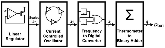
Figure 3.
Overall architecture of the proposed PPG readout IC. The photodiode driver, linear regulator, and embedded quantizer are integrated into a single loop to eliminate redundant DC suppression circuits.
3.2. Linear Regulator-Based Sensor Driver
The detailed implementation of the sensor driver is illustrated in Figure 4. A PMOS pass device regulates the photodiode bias voltage, ensuring stable sensor operation across a wide current range. The photodiode current is split into two parts: the DC component flows through the main transistor to maintain bias, while the AC component is mirrored to a scaled-down branch for sensing. This dual role of the regulator—both biasing and current partitioning—removes the need for external suppression circuits. As a result, overall power consumption is reduced while maintaining wide dynamic range.
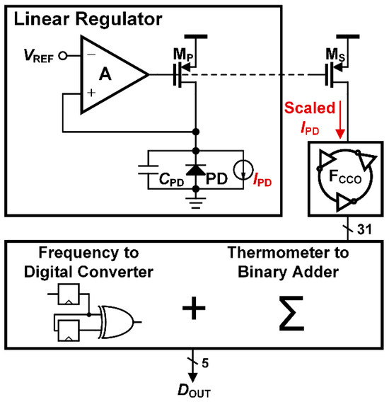
Figure 4.
Linear regulator-based sensor driver. The main transistor regulates the photodiode bias voltage, while a mirrored branch extracts the AC signal component for subsequent quantization.
3.3. Embedded VCO-Based Quantizer
The signal path includes a current-controlled oscillator (CCO), as shown in Figure 5. The mirrored AC current modulates the oscillation frequency of the CCO, which consists of cascaded inverter stages. The frequency variation is then digitized by a frequency-to-digital converter (FDC). This time-domain approach offers several advantages:
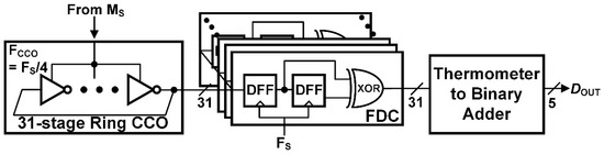
Figure 5.
Embedded VCO-based quantizer. The mirrored AC current modulates the frequency of a current-controlled oscillator, and the output is digitized by a frequency-to-digital converter with inherent noise-shaping properties.
- The quantizer exhibits inherent first-order noise shaping, improving accuracy for small signals.
- The direct current-to-frequency conversion avoids the inefficiencies of current-to-voltage conversion required in TIA-based circuits.
- The digital nature of the output simplifies subsequent processing and is robust against analog mismatches.
3.4. Mirroring Scale Calibrator
Process and temperature variations cause frequency drift in the oscillator, which can degrade readout accuracy. To compensate, the proposed design incorporates a mirroring scale calibrator, shown in Figure 6. The calibrator dynamically adjusts the effective transistor sizing in the current mirror branch. A digital counter monitors the oscillator frequency, and when deviation from the target frequency is detected, the counter incrementally enables or disables unit transistors in the mirrored branch. This counting-based resizing mechanism ensures stable oscillation frequency without analog trimming. As a result, the system maintains consistent performance across corners and environmental variations, while adding negligible power and area overhead.
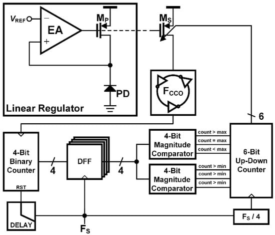
Figure 6.
Detailed schematic of the mirroring scale calibrator. The calibration circuit dynamically adjusts the scaling branch through a counting-based sizing mechanism, compensating for process and temperature variations to stabilize oscillation frequency.
4. Performance Evaluation
The proposed PPG readout IC was verified through extensive post-layout simulations in a standard 250 nm CMOS process. Simulations were performed across typical operating conditions as well as process–voltage–temperature (PVT) variations to evaluate robustness. The results demonstrate that the circuit achieves both ultra-low power consumption and wide dynamic range while maintaining stable operation under diverse conditions.
4.1. Output Spectrum Across Process Corners
Figure 7 presents the simulated output spectrum of the proposed readout across multiple process (Figure 7a) corners (SS, FF, SF, and FS) and (Figure 7b) temperature. In each case, the photodiode current was modeled as a sinusoidal input signal riding on a large DC bias. The results confirm that the embedded quantizer consistently achieves high signal-to-noise-and-distortion ratio (SNDR) and maintains spectral integrity regardless of corner conditions. This robustness highlights the effectiveness of the mirroring scale calibrator in compensating frequency drift.
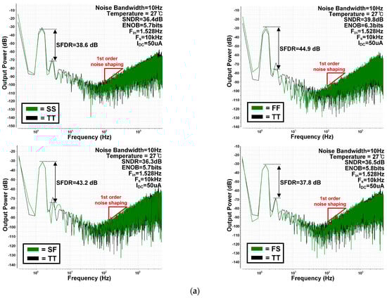
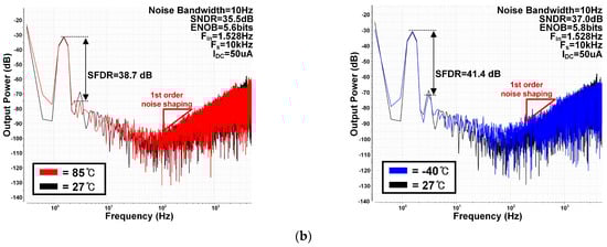
Figure 7.
Simulated output spectrum of the proposed PPG readout circuit across process (a) corners (SS, FF, SF, FS) and (b) temperature confirming robustness against process variations.
4.2. Output Spectrum Under Different DC Currents
The impact of varying photodiode DC bias current on signal quality was also examined. Figure 8 shows the output spectrum for DC current levels of 1 µA, 10 µA, 50 µA and 100 µA. Across this wide operating range, the AC signal is accurately captured without distortion, and the noise floor remains low. These results verify that the circuit maintains a wide dynamic range without requiring external suppression loops, making it well-suited for wearable sensors that encounter large variations in ambient light conditions.
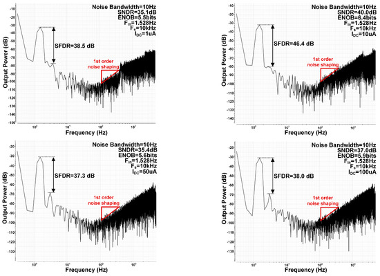
Figure 8.
Simulated output spectrum under different DC bias currents (1 µA, 10 µA, 50 µA, and 100 µA). The quantizer maintains high accuracy across a wide operating range.
4.3. SNDR Versus DC Current
Figure 9 plots the SNDR as a function of DC current. The curve demonstrates that the readout achieves stable performance across a broad bias range, with SNDR values consistently above 35 dB even at the extremes. This confirms that the architecture effectively isolates the useful AC component from the large DC offset inherent in photodiode outputs.
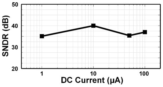
Figure 9.
Simulated SNDR versus DC current, demonstrating consistent performance and wide dynamic range.
4.4. Transient Response
Figure 10 evaluates the transient behavior of the sensor driver when subjected to sudden changes in photodiode current. Both load-transient and line-transient conditions were simulated. The regulator recovers rapidly from step changes in sensor current while maintaining output voltage stability. This fast response ensures reliable biasing of the photodiode under dynamic physiological conditions, such as abrupt motion or illumination changes.
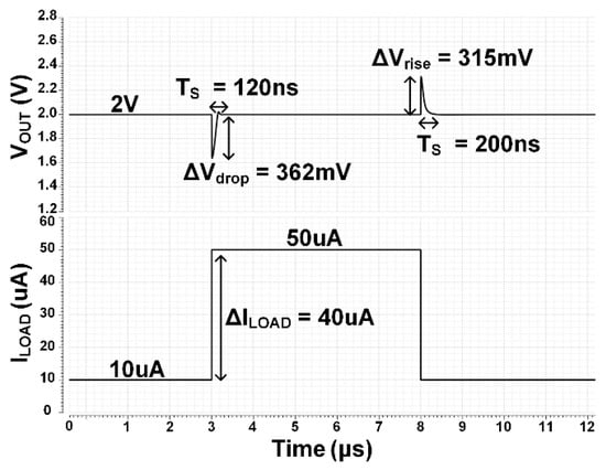
Figure 10.
Transient response of the proposed driver under sudden changes in photodiode current, showing fast recovery and stable regulation.
4.5. Load Regulation
The load regulation characteristics are shown in Figure 11. As the load current increases from 100 nA to 35 mA, the regulated output voltage drops only marginally (from 2.0002 V to 1.9996 V), corresponding to 0.03% deviation. This excellent regulation demonstrates that the driver can reliably support wide load variations while minimizing voltage fluctuation, a key requirement for low-noise PPG sensing.
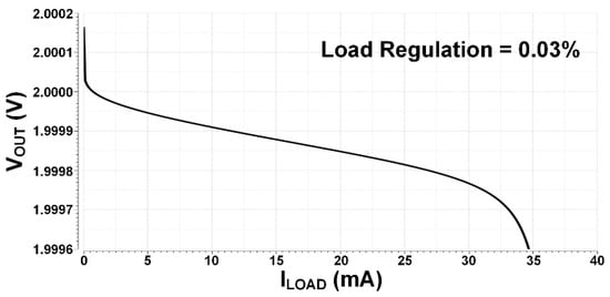
Figure 11.
Simulated load regulation characteristics of the linear regulator, with less than 0.03% deviation from 100 nA to 35 mA.
4.6. Area and Power Efficiency
The complete layout of the proposed readout IC is presented in Figure 12a. The design occupies a compact area of 0.725 mm2, making it suitable for integration in multi-channel sensor systems. The small footprint, combined with ultra-low power operation, enables deployment in space- and energy-constrained wearable platforms. Figure 12b presents the power breakdown of the proposed readout. As shown, the time-based quantizer dominates the power usage, accounting for approximately 66% of the total. The 31-stage current-controlled oscillator contributes about 29%, while the calibration circuit consumes only 5%.
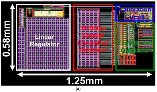
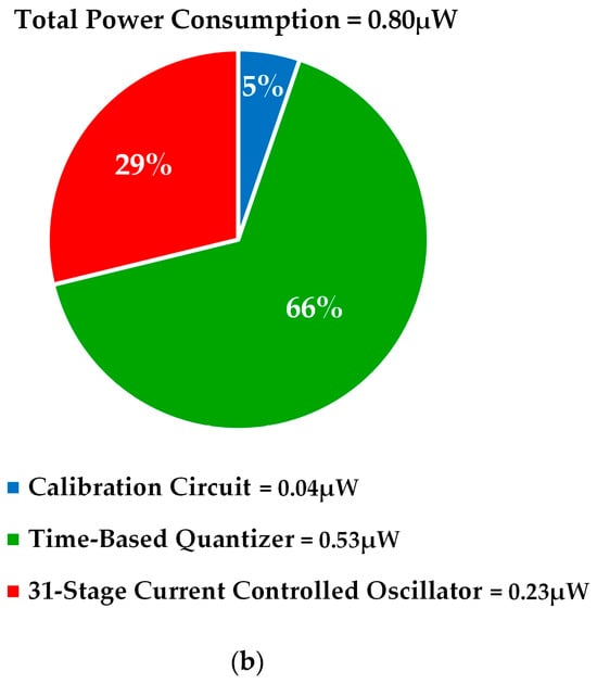
Figure 12.
(a) Layout of the proposed PPG readout IC, showing a compact design with total area of 0.725 mm2 and (b) presents the power breakdown of the proposed PPG readout IC.
4.7. Performance Summary and Comparison
A summary of the circuit performance is provided in Table 1, which compares the proposed work against representative prior state-of-the-art designs. The results clearly show that the design achieves superior energy efficiency, with a figure-of-merit (FoM) of 50.0 dB/µW, significantly outperforming recent TIA- and LDC-based solutions. Unlike previous architectures that require dedicated suppression loops, the proposed readout eliminates redundant current paths while delivering competitive SNDR and area efficiency.

Table 1.
Performance comparison.
5. Discussion
A major noise source in PPG readout circuits is DC variation (drift) due to ambient light changes and motion artifacts. In the proposed design, the linear regulator absorbs the large DC component while the VCO-based quantizer with inherent noise shaping extracts the AC signal robustly. This approach mitigates DC drift without requiring an explicit cancelation loop.
The simulation results confirm that the proposed readout architecture achieves a unique combination of low power, wide dynamic range, and robustness across variations. Several design choices contribute to these outcomes. First, integrating the quantizer within the sensor driver avoids redundant current paths and eliminates the need for explicit DC suppression, leading to an ultra-low power consumption of only 0.80 µW. This is significantly lower than recent TIA- and LDC-based circuits, as highlighted in Table 1. Second, the use of a mirroring scale calibrator ensures that the oscillator frequency remains stable against process and temperature variations, a challenge that commonly limits time-based quantizers. The counting-based resizing mechanism requires only minimal digital overhead yet provides substantial improvement in stability.
Another critical advantage is the figure-of-merit (FoM) achieved. The design reports 50.0 dB/µW, a value that is orders of magnitude higher than many previously published circuits. This metric demonstrates that the proposed solution delivers superior energy efficiency without sacrificing accuracy. Moreover, the inclusion of PVT corner simulations and DC current sweeps underscores the robustness of the approach, giving confidence that the architecture will perform reliably in real-world wearable environments where conditions vary continuously.
While the present work focuses on single-channel operation, the compact area (0.725 mm2) leaves ample room for scaling to multi-channel implementations in future work. Furthermore, the digital-friendly output of the VCO-based quantizer aligns well with system-on-chip integration, enabling straightforward coupling with digital signal processors for feature extraction. Overall, the architecture bridges the gap between traditional analog-intensive designs and modern low-power, time-domain approaches.
6. Conclusions
This paper presented a low-power, a wide-dynamic-range PPG readout IC that integrates a VCO-based quantizer directly into the photodiode driver, extended from [24]. By eliminating the need for a dedicated DC suppression circuit, the proposed design achieves both reduced power consumption and simplified architecture. The linear regulator-based driver manages the DC component efficiently, while the embedded quantizer digitizes the AC signal with first-order noise shaping. A novel mirroring scale calibrator stabilizes oscillator frequency against process and temperature variations through a counting-based transistor sizing mechanism.
Post-layout simulations demonstrated that the readout achieves an SNDR of 40.0 dB at 10 µA bias current while consuming less than 1 µW from a 2.5 V supply. The circuit maintained high performance across PVT corners and over a wide range of DC currents, validating its robustness. With an occupied area of only 0.725 mm2, the design is well-suited for wearable and biomedical sensing platforms that demand compactness and energy efficiency.
Compared to prior works, the proposed architecture delivers a substantially improved energy efficiency figure-of-merit, making it a strong candidate for integration in next-generation health monitoring devices. Future work will explore multi-channel implementations and chip-level measurements to further validate the design in practical applications. In particular, multi-channel integration requires addressing challenges such as channel-to-channel interference, increased power consumption, and synchronization of parallel readout paths. In addition, chip fabrication and measurement with real PPG sensors will be carried out to verify robustness under varying ambient conditions and user motion, ensuring practical applicability in wearable healthcare systems. Furthermore, multi-channel operation will necessitate enhanced digital back-end processing, including higher data throughput and adaptive algorithms for artifact reduction.
Author Contributions
Conceptualization, H.J.; writing—original draft preparation, H.N.; writing—review and editing, H.N.; visualization, W.K.; supervision, Y.K.; project administration, S.-T.K. All authors have read and agreed to the published version of the manuscript.
Funding
This research was supported by National R&D Program through the National Research Foundation of Korea (NRF) funded by Ministry of Science and ICT (No. RS-2020-NR047143) and Korea Planning & Evaluation Institute of Industrial Technology (RS-2024-00420538) grant funded by the Ministry of Trade, Industry & Energy (MOTIE).
Data Availability Statement
The original contributions presented in this study are included in the article. Further inquiries can be directed to the corresponding author.
Acknowledgments
This work was supported by Chungbuk National University NUDP program (2025). The EDA tool was supported by the IC Design Education Center (IDEC), Republic of Korea.
Conflicts of Interest
Author Yongkwon Kim was employed by the company NUCARE, Inc. The remaining authors declare that the research was conducted in the absence of any commercial or financial relationships that could be construed as a potential conflict of interest.
References
- Ebrahimi, Z.; Gosselin, B. Ultralow-Power Photoplethysmography (PPG) Sensors: A Methodological Review. IEEE Sens. J. 2023, 23, 16467–16480. [Google Scholar] [CrossRef]
- Biswas, D.; Simões-Capela, N.; Van Hoof, C.; Van Helleputte, N. Heart Rate Estimation from Wrist-Worn Photoplethysmography: A Review. IEEE Sens. J. 2019, 19, 6560–6570. [Google Scholar] [CrossRef]
- Chettri, N.; Aprile, A.; Bonizzoni, E.; Malcovati, P. Advances in PPG Sensors Data Acquisition with Light-to-Digital Converters: A Review. IEEE Sens. J. 2024, 24, 25261–25274. [Google Scholar] [CrossRef]
- Kim, K.B.; Baek, H.J. Photoplethysmography in Wearable Devices: A Comprehensive Review of Technological Advances, Current Challenges, and Future Directions. Electronics 2023, 12, 2923. [Google Scholar] [CrossRef]
- Asada, H.H.; Shaltis, P.; Reisner, A.; Rhee, S.; Hutchinson, R.C. Mobile monitoring with wearable photoplethysmographic biosensors. IEEE Eng. Med. Biol. Mag. 2003, 22, 28–40. [Google Scholar] [CrossRef] [PubMed]
- Wang, K.; Tan, B.; Wang, X.; Qiu, S.; Zhang, Q.; Wang, S.; Yen, Y.T.; Jing, N.; Liu, C.; Chen, X.; et al. Machine learning-assisted point-of-care diagnostics for cardiovascular healthcare. Bioeng. Transl. Med. 2025, 10, e70002. [Google Scholar] [CrossRef] [PubMed]
- Vashishtha, P.; Kofler, C.; Verma, A.K.; Giridhar, S.P.; Tollerud, J.O.; Dissanayake, N.S.L.; Gupta, T.; Sehrawat, M.; Aggarwal, V.; Mayes, E.L.H.; et al. Epitaxial interface-driven photoresponse enhancement in monolayer WS2–MoS2 lateral heterostructures. Adv. Funct. Mater. 2025, 35, e12962. [Google Scholar] [CrossRef]
- Prajapat, P.; Vashishtha, P.; Gupta, G. High-temperature resilient neuromorphic device based on optically configured monolayer MoS2 for cognitive computing. Small 2025, 21, 2411596. [Google Scholar] [CrossRef] [PubMed]
- Winokur, E.S.; O’Dwyer, T.; Sodini, C.G. A Low-Power, Dual-Wavelength Photoplethysmogram (PPG) SoC with Static and Time-Varying Interferer Removal. IEEE Trans. Biomed. Circuits Syst. 2015, 9, 581–589. [Google Scholar] [CrossRef] [PubMed]
- Alamouti, S.F.; Jan, J.; Yalcin, C.; Ting, J.; Arias, A.C.; Muller, R. A Sparse Sampling Sensor Front-End IC for Low Power Continuous SpO2 & HR Monitoring. IEEE Trans. Biomed. Circuits Syst. 2022, 16, 997–1007. [Google Scholar] [PubMed]
- Lee, Y.; Lee, H.; Jang, J.; Lee, J.; Minseo, K.; Jaehyuk, L.; Kim, H.; Lee, K.R.; Yoo, H.-J.; Yoo, S.; et al. 22.3 A 141 µW Sensor SoC on OLED/OPD Substrate for SpO2/ExG Monitoring Sticker. In Proceedings of the 2016 IEEE International Solid-State Circuits Conference (ISSCC), San Francisco, CA, USA, 31 January–4 February 2016; pp. 384–385. [Google Scholar]
- Lin, B.; Ma, Z.; Atef, M.; Ying, L.; Wang, G. Low-Power High-Sensitivity Photoplethysmography Sensor for Wearable Health Monitoring System. IEEE Sens. J. 2021, 21, 16141–16151. [Google Scholar] [CrossRef]
- Agarwala, R.; Wang, P.; Bishop, H.L.; Dissanayake, A.; Calhoun, B.H. A 0.6 V 785-nW Multimodal Sensor Interface IC for Ozone Pollutant Sensing and Correlated Cardiovascular Disease Monitoring. IEEE J. Solid-State Circuits 2021, 56, 1058–1070. [Google Scholar] [CrossRef]
- Marefat, F.; Erfani, R.; Kilgore, K.L.; Mohseni, P. A 280 μW, 108 dB DR PPG-Readout IC with Reconfigurable, 2nd-Order, Incremental ΔΣM Front-End for Direct Light-to-Digital Conversion. IEEE Trans. Biomed. Circuits Syst. 2020, 14, 1183–1194. [Google Scholar] [CrossRef] [PubMed]
- Lin, Q.; Xu, J.; Guo, Z.; Choi, J.; Li, X.; Zhen, Z.; Wang, G.; Yuan, J.; Tang, X.; Chen, J.; et al. A 119 dB Dynamic Range Charge Counting Light-to-Digital Converter for Wearable PPG/NIRS Monitoring Applications. IEEE Trans. Biomed. Circuits Syst. 2020, 14, 800–810. [Google Scholar] [CrossRef] [PubMed]
- Lin, Q.; Xu, J.; Guo, Z.; Choi, J.; Li, X.; Zhen, Z.; Wang, G.; Yuan, J.; Tang, X.; Chen, J.; et al. A 196 μW, Reconfigurable Light-to-Digital Converter with 119 dB Dynamic Range, for Wearable PPG/NIRS Sensors. In Proceedings of the 2019 Symposium on VLSI Circuits, Kyoto, Japan, 9–14 June 2019; pp. C58–C59. [Google Scholar]
- Lin, Q.; Xu, J.; Guo, Z.; Choi, J.; Li, X.; Zhen, Z.; Wang, G.; Yuan, J.; Tang, X.; Chen, J.; et al. A 134 dB Dynamic Range Noise Shaping Slope Light-to-Digital Converter for Wearable Chest PPG Applications. IEEE Trans. Biomed. Circuits Syst. 2021, 15, 1224–1235. [Google Scholar] [CrossRef] [PubMed]
- Gao, Y.-H.; Li, J.; Fan, C.-H.; Leung, K.N.; Zhang, Y.-T.; Pun, K.-P. A 9.84-μW 148.9-dB Total DR Light-to-Digital Converter with Current-Integration SAR Quantizer for Multi-Wavelength PPG Applications. IEEE Trans. Circuits Syst. I Regul. Pap. 2025, 1–14. [Google Scholar] [CrossRef]
- Park, M.; Perrott, M.H. A 78 dB SNDR 87 mW 20 MHz Bandwidth Continuous-Time ΔΣ ADC with VCO-Based Integrator and Quantizer Implemented in 0.13 μm CMOS. IEEE J. Solid-State Circuits 2009, 44, 3344–3358. [Google Scholar] [CrossRef]
- Reddy, K.; Park, M.; Lee, S.; Elshazly, A.; Hanumolu, P.K.; Perrott, M.H. A 16 mW 78 dB-SNDR 10 MHz-BW CT-ΔΣ ADC Using Residue-Cancelling VCO-Based Quantizer. In Proceedings of the 2012 IEEE International Solid-State Circuits Conference (ISSCC), San Francisco, CA, USA, 19–23 February 2012; pp. 152–154. [Google Scholar]
- Kim, J.; Jang, T.-K.; Yoon, Y.-G.; Cho, S. Analysis and Design of Voltage-Controlled Oscillator Based Analog-to-Digital Converter. IEEE Trans. Circuits Syst. I Regul. Pap. 2010, 57, 18–30. [Google Scholar]
- Nguyen, V.; Schembari, F.; Staszewski, R.B. Exploring Speed Maximization of Frequency-to-Digital Conversion for Ultra-Low-Voltage VCO-Based ADCs. IEEE Trans. Circuits Syst. I Regul. Pap. 2023, 70, 1043–1056. [Google Scholar] [CrossRef]
- Borgmans, J.; Sacco, E.; Rombouts, P.; Gielen, G. Methodology for Readout and Ring Oscillator Optimization Toward Energy-Efficient VCO-Based ADCs. IEEE Trans. Circuits Syst. I Regul. Pap. 2022, 69, 985–998. [Google Scholar] [CrossRef]
- Noh, H.; Kim, W.; Jeon, H. A Low Power, Wide Dynamic Range PPG Readout IC with Time-Based Quantizer Embedded in Photodiode Driver Circuits. In Proceedings of the 2025 IEEE 68th International Midwest Symposium on Circuits and Systems (MWSCAS), Lansing, MI, USA, 10–13 August 2025; pp. 641–644. [Google Scholar]
Disclaimer/Publisher’s Note: The statements, opinions and data contained in all publications are solely those of the individual author(s) and contributor(s) and not of MDPI and/or the editor(s). MDPI and/or the editor(s) disclaim responsibility for any injury to people or property resulting from any ideas, methods, instructions or products referred to in the content. |
© 2025 by the authors. Licensee MDPI, Basel, Switzerland. This article is an open access article distributed under the terms and conditions of the Creative Commons Attribution (CC BY) license (https://creativecommons.org/licenses/by/4.0/).