Article

A Simple Burst-Mode Multiple-Entropy TRNG Based on Standard Logic Primitives

by
Bartosz Mikołaj Szkoda
and
Piotr Zbigniew Wieczorek
*
Faculty of Electronics and Information Technology, Institute of Electronics Systems, Warsaw University of Technology, 00-665 Warsaw, Poland
*
Author to whom correspondence should be addressed.
Electronics 2025, 14(19), 3803; https://doi.org/10.3390/electronics14193803
Submission received: 4 September 2025 / Revised: 22 September 2025 / Accepted: 22 September 2025 / Published: 25 September 2025

Abstract

The paper introduces the concept of a True Random Number Generator (TRNG) based on an unstable circuit that uses only two types of logic devices: XOR gates and logic inverters forming delay lines. The core circuit ensures randomness in both the voltage (logical state) and time domains (duration of autonomous operation), while utilizing very few resources. Due to its low complexity, the proposed TRNG can be easily implemented in reconfigurable devices without sophisticated components such as Digital Clock Managers (DCM), Phase Locked Loops (PLL), or dedicated IP cores. The authors present a theoretical analysis of the TRNG using a Simulink macromodel, demonstrating chaotic behavior, and describe its implementation on a Complex Programmable Logic Device (CPLD) and additional verification on an FPGA. The randomness quality of the TRNG was validated using the standard National Institute of Standards and Technology (NIST) SP 800-22 battery of tests.

1. Introduction

The generation of truly random numbers is one of the critical factors that guarantee the security of cryptographic systems. In many practical applications, such as digital bank transfers, credentials storage, private calls, or even voting systems, encryption algorithms are fed an initial number called a seed. If an encryption algorithm is known (which is usually the case), it is of great importance to ensure the infeasibility of predicting the seed value, as it is one of the key obstacles for potential attackers attempting to steal the data.
In particular, this was the case for Netscape’s web browser in 1995, where seeds were based on three predictable variables–process ID, parent process ID, and time of the day [1]. The team responsible for the discovery of the vulnerability was able to cleverly narrow down the possible range of values for these variables to such an extent that a brute-force attack became feasible. In a matter of minutes, the encrypted data became available in plain text to the attackers.
Some seemingly “random” numbers are actually deterministic and predictable, as they are a result of an intentionally complex computation. Because of this property, we differentiate between pseudo-random and truly random numbers. Pseudo-random seeds used in Netscape’s browser were the root cause of the system’s compromise.
The generation of truly random numbers using solely software is impossible. Software is intrinsically deterministic, just as the CPU that is running it. The only way to acquire a truly random number is by sampling a physical variable that is unpredictable by nature. A peculiar example is Lavarand—a rack of lava lamps that produces a visual pattern that is then used to generate a truly random seed [2]. However, simply sampling electrostatic noise with an analog-to-digital converter might do the trick in most cases. Companies may include dedicated hardware in their products just to produce truly random numbers based on a physical source of entropy, which shows the importance of truly random numbers for digital use cases. For example, Intel CPUs have an instruction RDRAND (read random), the sole purpose of which is to return a random number from a source of entropy located within the chip [3,4].
Because some random numbers are better than others, one of the standard ways to assess this is to collect a large set of random numbers produced by the generator and use the NIST SP 800-22 test battery [5]. Usually, statistical measures of randomness will be more favorable for more complex systems. Some use cases, however, will have scarce resources while having equal demand for high-quality randomness. A cheap and compact True Random Number Generator (TRNG) will find a multitude of applications in devices that have few assets but require cryptographic security, notably in the fast-growing branch of the Internet of Things [6]. TRNGs are also crucial in medical applications utilizing lightweight IoT solutions [7].

1.1. Modern Solutions for TRNGs

Modern solutions exploit many different sources of entropy. However, with regard to our work, the most related and common are jitter (phase noise), metastability, and chaos. Signal jitter is present in real and periodic signals and manifests itself as an unpredictability of the precise moment of signal edges [8,9,10,11,12,13,14,15,16,17,18,19,20,21,22,23]. Each individual edge is subject to a deviation; thus, it is almost always slightly off its expected position. Metastability occurs when timing restrictions (notably setup and hold times) of bistable elements, such as Flip-Flops (FF), are violated, resulting in unpredictable outputs [15,20,22,24,25,26,27,28]. Chaos is a property of non-linear, dynamical systems, which behave in a highly unpredictable manner in time, and their dynamics are sensitive to initial values. Even a slight difference can drastically alter the results due to the sensitivity of differentials that describe the non-linear system to an initial condition [27,29,30,31,32,33,34].
Ring Oscillators (ROs) are used extensively in solutions that harvest randomness from jitter. An RO is an easily implementable square wave generator. It is a closed loop of an odd number of inverters, operating indefinitely. Each inverter introduces a slight phase deviation during each signal pulse (i.e., rising or falling slope).
The quality of RO randomness requires sufficient jitter accumulation, as stated in [8]. The authors point out that high randomness from this source requires either a high-order RO (in this case, the order is the number of inverters within the oscillator), thus decreasing the throughput, or a low-order RO accumulating jitter for a long period of time, which reduces the RO frequency, which in turn affects the throughput. The authors tackle the issue by an extended design of RO that includes additional feedback, which results in a much higher oscillation frequency for the same order of RO. The additional feedback is added to every inverter in the RO chain. It is realized by negating the current inverter’s output and applying NAND operation with a feedback signal from the next inverter in the chain. In such a solution, the randomness of two Multi-Stage Feedback Ring Oscillators is extracted by using their output as a clock for the D-type FFs (DFFs), and an analog Phase-Locked Loop (PLL) signal as data. Eventually, the FF outputs are XORed together, and truly random numbers are produced.
An example of a solution with jitter-based entropy without using complex clocking primitives like the analog PLL is described in [9]. The authors design a variant of ROs based on an All Digital PLL (ADPLL) using only basic digital logic components. An important part of the ADPLL that is ultimately responsible for producing the jitter is a Digitally Controlled Oscillator (DCO) composed of NOR gates and a D-type FF. The TRNG is designed by combining multiple ADPLLs operating at different frequencies, set up in parallel. The ADPLL outputs are sampled by DFFs, XORed, and post-processed by another XOR-based logic.
Another solution based on the ROs, described in [10], uses an RO with a latch in the loop. Depending on the control signals applied to the latch, the output is either stable, metastable, or oscillating. The TRNG relies mainly on jitter accumulation of multiple parallel latched ROs working in oscillating mode. After a predefined number of cycles, the ROs are stopped by applying a proper control signal to the latch. The output logical states of ROs—that are unpredictable due to jitter—are sampled. The samples are then XORed together before outputting the final random number.
In [11] a Cross Coupled XOR gate (CCX) and a Braided XOR Logic Gate (B-XOR-LG) network are combined to create a TRNG. A CCX has multiple modes of operation, depending on the pair of input control signals. They can work as ROs (oscillating), remain in the stable solution, or have an unpredictable logical state. Thus, to cover the entire range of operating modes, the authors routed two equal-length ROs to the inputs of CCX to use them as a source of all input pair combinations. The CCX outputs are connected to B-XOR-LG, which is a set of XOR gates with an intricate network of connections (couplings, feedbacks, etc.). This network enables race-hazard (different outcomes for different timings of applied signals) as an entropy source. The outputs are sampled with FFs and post-processed with an XOR gate.
A solution that utilizes a Xilinx Digital Clock Manager (DCM) primitive together with a carry-chain primitive (i.e., CARRY4) is described in [25]. These components are used to achieve timing violations of subsequent DFFs responsible for sampling the delayed clock signal while synchronous to the original clock, thus putting them in a metastable state. The DCM has a programmable phase delay of a clock signal. The CARRY4 primitive is used to gain even higher granularity of the phase delay by exploiting its internal multiplexer, which has different delays for different outputs. The outputs of CARRY4 are connected to four DFFs. A finite state machine automatically detects if the FFs operate in the metastable range by adjusting the phase offset while observing the outputs of the DFFs. An additional source of entropy comes from a race condition generated by the loopback of CARRY4 outputs back to the selector inputs of the carry-chain’s multiplexers. The signals are then XORed, concatenated into a 32-bit vector, and post-processed using simple arithmetic and conditional binary operations.
A hybrid approach is proposed in [24] that combines jitter- and metastability-based entropy sources. The TRNG consists of multiple self-feedback multiplexers that are fed with combinations of different-order ROs signals. In this case, the self-feedback means that the output of MUX is connected to its address input. Due to such wiring, the MUX output switches constantly between inputs with ROs’ jittered signals. This also sporadically causes a transient, settling signal at the output that results in the metastability of the subsequent sampling DFFs. The random numbers are acquired by XORing together FFs’ outputs. The hybrid approach allowed the ring oscillators to operate at high speeds, resulting in a TRNG that passed the randomness tests, with high throughput and low resource utilization [24].
Another hybrid approach (jitter+metastability) is presented in [26]. This work also exploits a structure of Cross-Coupled XOR gates that are connected in series to create a Dual CCX (DCCX). As mentioned previously, a CCX has various working modes depending on input signals. Hence, in Dual CCX, the first CCX is used in oscillatory mode to excite subsequent cross-coupled gates with all combinations of input signal pairs. This, in turn, results in jittered oscillations or unpredictable signal values that cause metastability of the sampling circuit. For the purposes of TRNG, multiple DCCXs are operating in parallel. Their outputs are captured by DFFs, and samples are XORed for a final post-processing.
There are multiple ways to exploit properties of chaotic systems for the generation of truly random numbers. In [32], particular 1-D chaotic maps are designed as three-transistor topologies in a 45 nm CMOS process for a solution directly implementable in silicon. A method of cascading them together is proposed to improve their statistical properties related to randomness. Finally, multiple parallel map configurations are put together. The map outputs are routed to comparators and XOR gates, thus completing the TRNG design. The results indicate a good randomness quality of the TRNG.
In [31], an analog chaotic circuit built of discrete components is implemented. The chaotic properties come from the nonlinear characteristics of a custom-manufactured memristor. A comparator is then fed with a signal from the chaotic circuit and a sinusoidal signal from a function generator. The resulting bitstream from the comparator produces Truly Random Numbers by means of NIST tests.
Chaotic systems may also be easily implemented digitally; however, the chaos usually becomes deterministic. A discretized model can be derived from differential equations that describe the system [35] and used in platforms such as an FPGA. In [29], a 3-D chaotic system is discretized for digital implementation in an FPGA. Samples of states of the system are post-processed with a function based on the El-Gamal encryption algorithm, which proves sufficient to make a TRNG.
A 5-D hyperchaotic system was implemented and various applications were explored in [30], notably a TRNG implementation using its digitized model. The outputs of the discretized system were XORed with RO outputs, resulting in a TRNG that passed randomness tests. In the solution, the RO was used to add an extra source of entropy and to avoid limiting throughput by providing a parallel source of random numbers to be XORed simultaneously with outputs from the chaotic system.
The provided solutions utilize various circuits to produce randomness in their TRNG implementations. Some aim to be compact and high-throughput, while others explore unconventional applications of various devices and systems. However, for practical purposes, the main theme in the majority of papers is to design a TRNG with low resource utilization using the simplest available components. This enables applications in low-power and low-resource devices.
In this work, we would like to present our approach to this problem by proposing Cross-Coupled XOR Gates with delay lines embedded in their outputs—a TRNG design that exploits multiple sources of entropy at once, uses very basic and very little resources in its implementation, and has a distinctive property of burst operation.
The rest of the paper is structured as follows. The TRNG concept is introduced in the remainder of this section. Then, in Section 2 we present a macromodel of the circuit, implementation on a CPLD, and data acquisition method. Section 3 shows the simulation, empirical, and statistical results. Finally, we conclude our work.

1.2. TRNG Core Concept

We propose a conceptually simple TRNG core (Figure 1) that consists of two parallel paths, each made up of an XOR gate connected to a digital delay line. The output of the delay line is then fed back to the input of the XOR gate from the corresponding path, but also crossed over to the input of the XOR gate at the adjacent path. This results in cross-coupling of the gates. The delay lines are chains of different buffering lengths, which are graphically represented by different widths of delay line blocks. The circuit stays in the idle state unless a pulse is fed to the input of one of the paths. The pulse travels then through the path and is mixed and XORed with a delayed version of itself from both paths again. Proper selection of the delay chain lengths results in finite, decaying oscillations. This can be explained by analyzing the circuit without the cross-coupling, with feedback only—the pulse XORing itself with its offset version results in chopping of the signal into thinner and thinner slices. Due to the limited frequency bandwidth of the circuit in real hardware, this will eventually result in fading of the ever-thinning slices, causing the circuit to stop. Cross-coupling allows the circuit to operate longer, because intensification of mixing of pulses from both paths results in short-period metastability that may temporarily cancel out thinning of the signal slices. Furthermore, in an ideal case (i.e., in a situation where no noise sources are present), the shape of waveforms would be deterministic and constant between realizations. However, implementation in real hardware introduces a multitude of randomness sources: electrical noise and temperature drift affecting switching of gates, process variations preventing repeatability of transfer functions, and jitter of delay paths. Due to these factors, the resulting waveforms are unique and random because the pulses arrive at the XOR gates at random times. To harvest this randomness, it is necessary to sample the resulting bitstream. This process is simply realized by acquiring the waveform at the output of one of the paths with an FF.
The blocks (primitives) used in the TRNG allow an easy implementation in programmable digital logic devices, notably in FPGAs or CPLDs. XOR gate implementation is very straightforward in Hardware Description Languages. Delay line behavior can be easily imitated by a cascade of inverter pairs. A result of the signal passing through a pair of inverters connected in series is the same signal (logically) but delayed due to finite propagation time. The delay value can be adjusted by increasing or decreasing the number of inverters.
Another important point is that this concept has a very simple structure compared to other methods. It requires no specialized components like PLL or DCM, runs on basic digital logic primitives, does not require any arithmetic blocks as in digitized chaotic systems, does not rely on external elements, has relatively high throughput, and—because it operates in bursts—it can be run on demand, thus saving power.

2. Materials and Methods

2.1. Macromodel of the TRNG Core

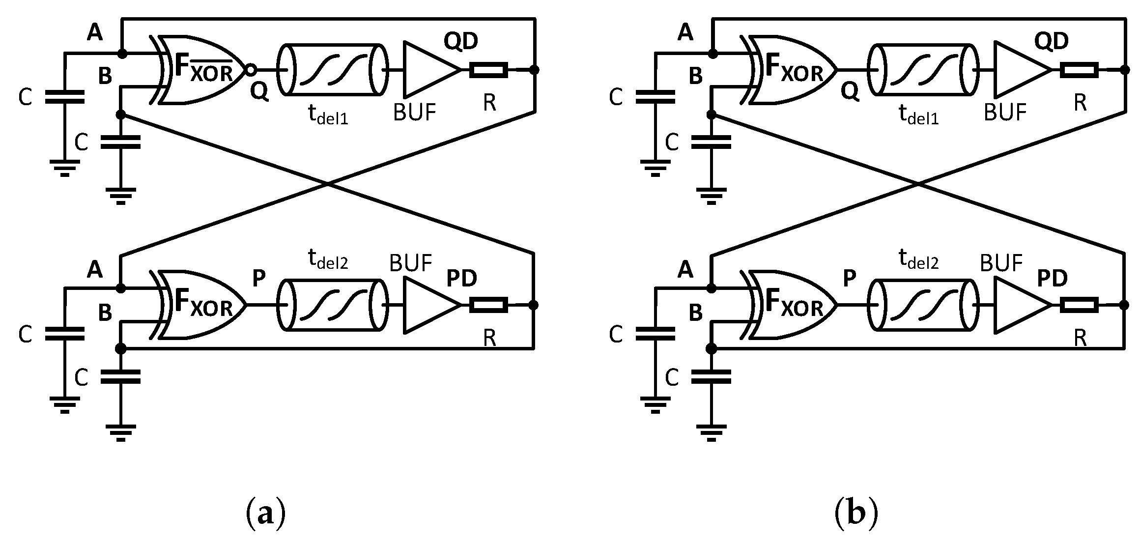
The proposed circuit was simplified (for the purpose of formal description) and modelled with the use of two nonlinear functions ( F X O R , F X O R ¯ ), namely logical gates with XOR (NXOR) transfer characteristics, two ideal delays ( t d e l 1 and t d e l 2 ), buffers with the output resistance (R), and X O R ( N X O R ) gates’ input capacitances. The circuit description depends on time, i.e., during the initial input pulse ( t 0 , t p u l s e ), the upper X O R gate acts as X N O R (see Figure 2a), which leads to the generation of a pulse, which in turn is further passed to the first delay line and the rest of the circuit.
Moreover, in the proposed TRNG core, the delay time t d e l 1 > t p u l s e ; therefore, the delayed output pulse at the node Q returns to the input A during the autonomous operation of the circuit.
When the time of operation t > t p u l s e , the circuit topology becomes symmetrical (see Figure 2b), and pulses returning from the PD and QD nodes increase the number of pulse appearances at the Q output. The dynamics of the proposed circuit are sophisticated, due to the F X O R , F X O R ¯ , F B U F gate nonlinearities, delays, and τ = R C inertia. These lead to a set of ordinary nonlinear delayed differentials (1).
U Q D ( t ) = F B U F U Q ( t t d e l 1 ) t 0 , t d e l 1 U Q D = 2 τ d U A ( t ) d t + U A ( t ) t 0 U P D ( t ) = F B U F U P ( t t d e l 2 ) t 0 , t d e l 2 U P D = 2 τ d U B ( t ) d t + U B ( t ) t 0 U Q ( t ) = F X O R ¯ ( U A ( t ) , U B ( t ) ) t 0 , t p u l s e U Q ( t ) = F X O R ( U A ( t ) , U B ( t ) ) t > t p u l s e U P ( t ) = F X O R ( U B ( t ) , U A ( t ) ) t 0
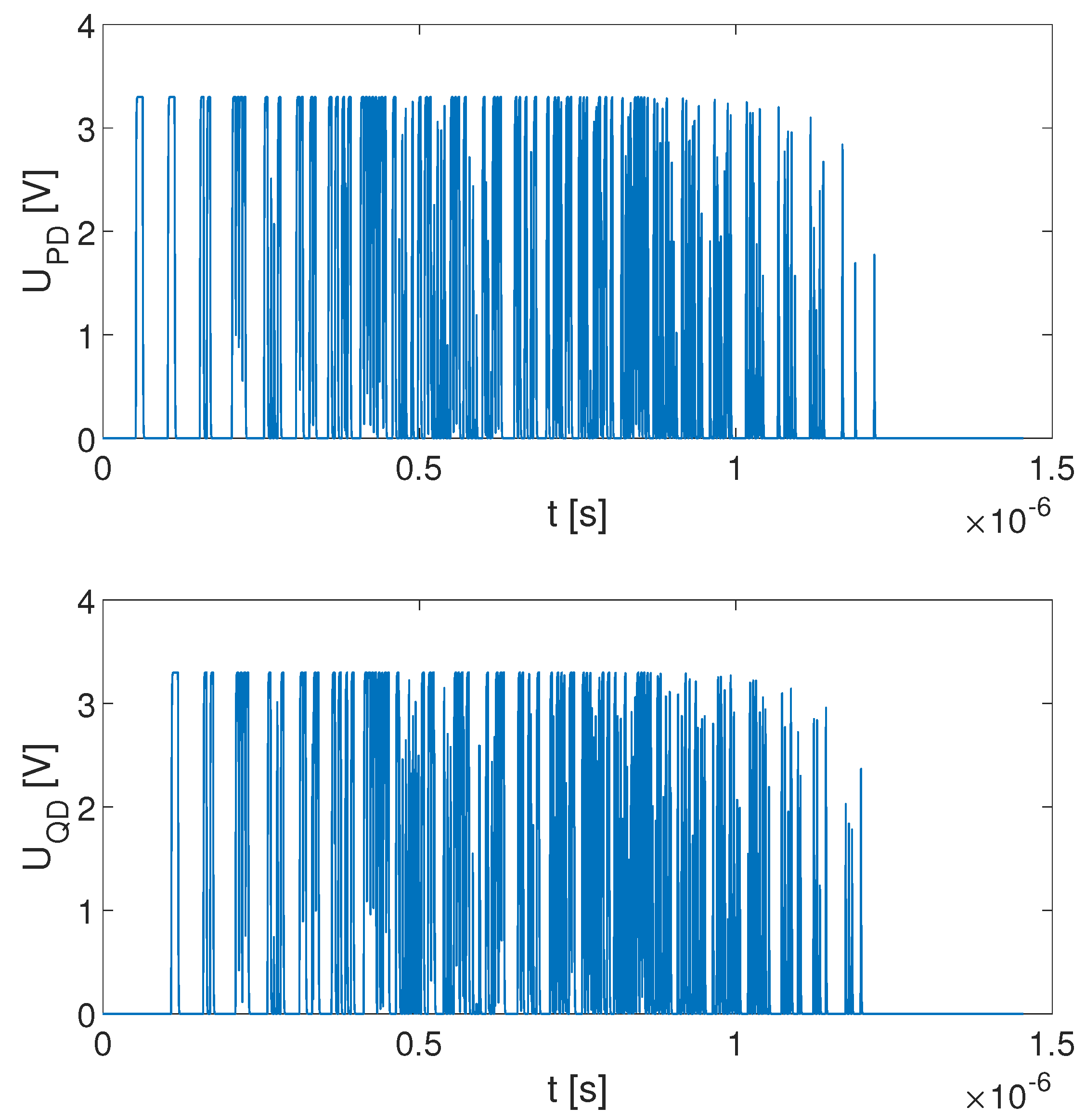
The macromodel shown in Figure 2 was subjected to numerical analysis performed in the Matlab R2024a Simulink environment, where the F X O R , F X O R ¯ functions and BUF devices were modelled with both the CMOS library blocks and sigmoid functions [36,37], which are suitable for behavioral modeling, i.e., F X O R U A , U B = V D D 2 ( 1 + tanh 1 2 tanh 2 2 U A ( t ) + U B ( t ) V D D , F X O R ¯ U A , U B = V D D F X O R U A , U B , F B U F U A , B = V D D 2 1 + tanh G U A , B V D D 2 . The solution for (1) over time depends heavily on t d e l 1 , t d e l 2 , τ , and to a lesser extent on G (gate transfer function slope). These parameters were adjusted to match the empirical behavior of the circuit core implemented in an Altera MAX V (see Section 2.2) [38]. The example response of the macromodel for t d e l 1 = 50 ns, t d e l 2 = 55 ns, τ = 0.16 ns, G = 12 , obtained with Matlab R2024a Simulink, for t p u l s e = 10 ns is shown in Figure 3.
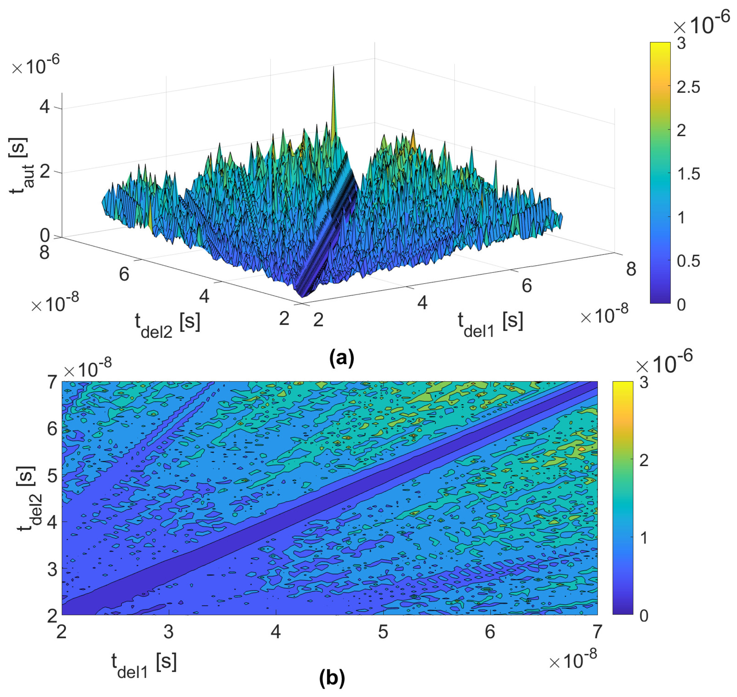
The circuit manifests fading oscillations, leading to a stable constant solution U Q D t = 0 , U P D t = 0 ; however, the response time of the system varies with t d e l 1 , t d e l 2 , and the initial condition U A t = 0 , U B t = 0 . In order to identify the relationship between the time of the autonomous range of operation ( t a u t ) of the system, and the t d e l 1 , t d e l 2 set, we performed a parametric simulation for variable t d e l 1 , t d e l 2 with U A t = 0 = 0 , U B t = 0 = 0 . The results presented in Figure 4a show that the proper choice is not obvious.
One can see on the contour plot (see Figure 4b) that local maxima are localized outside the t d e l 1 = t d e l 2 axis of symmetry, and higher t a u t values tend to appear when t d e l 1 and t d e l 2 are roughly > 45 ns.
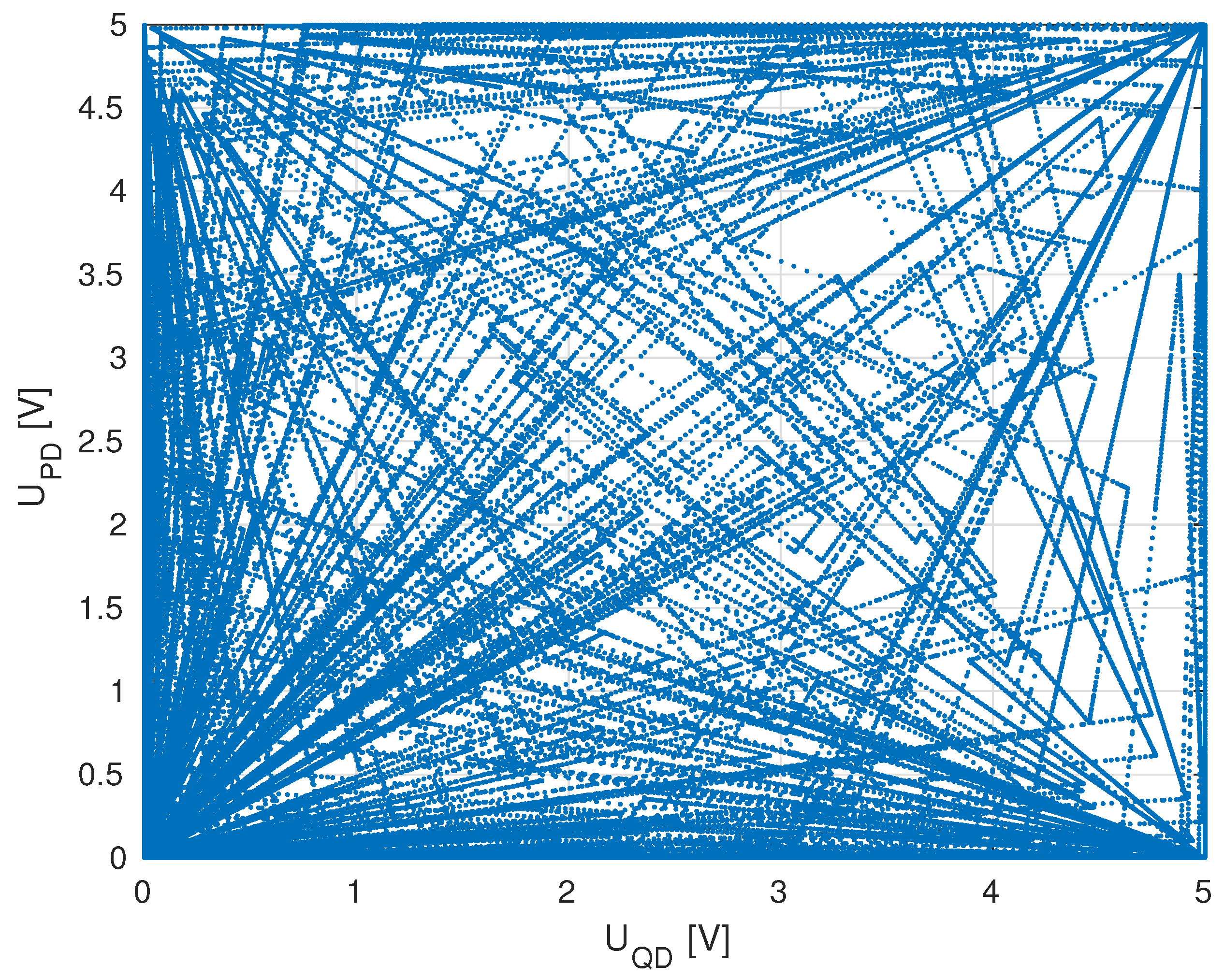
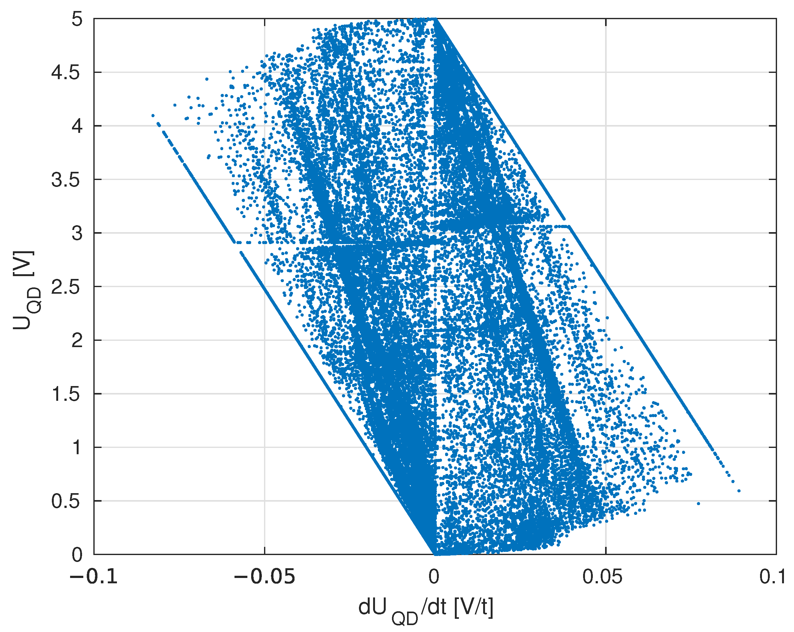
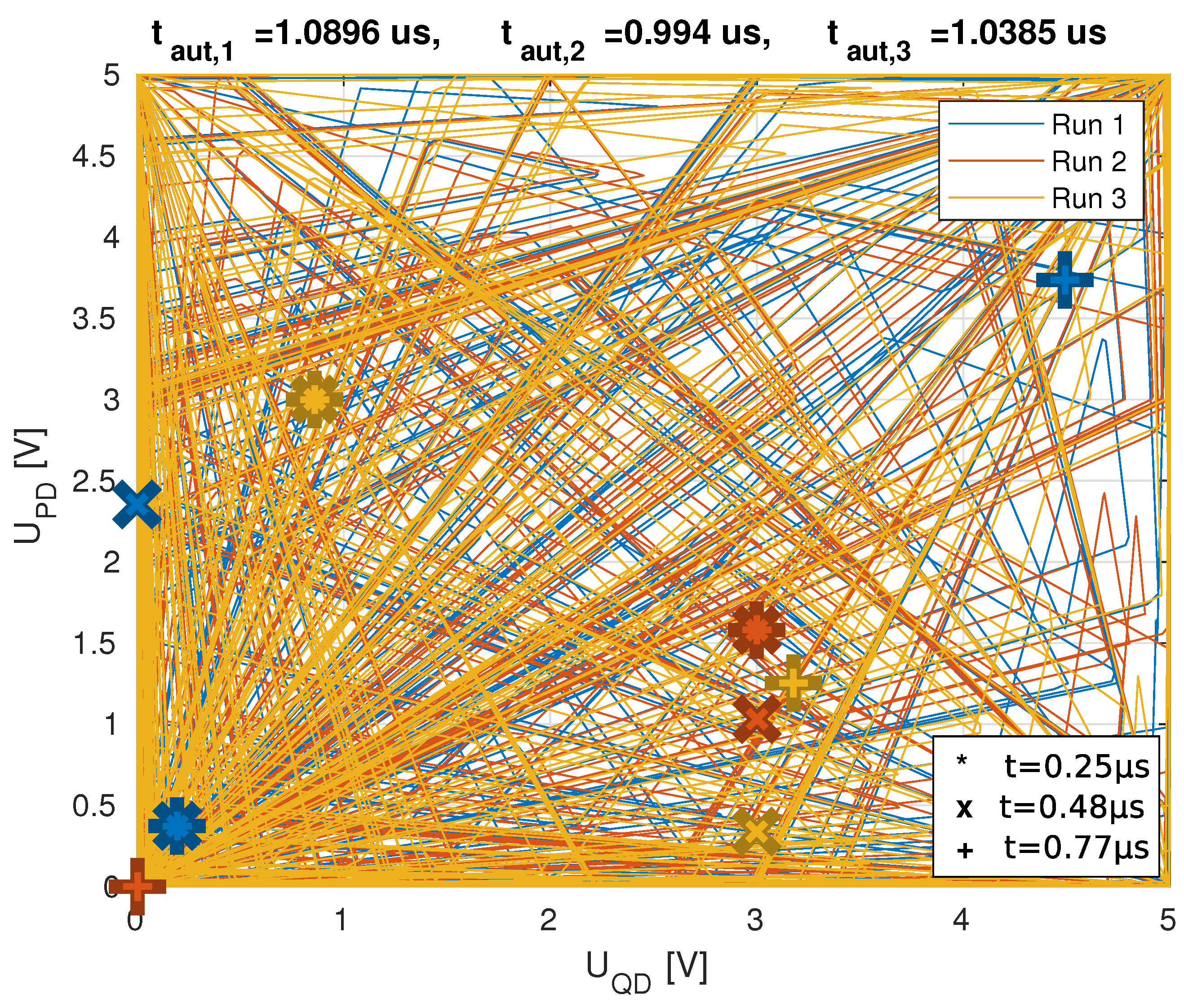
According to results obtained in the Matlab Simulink environment, t d e l 1 = 55 ns and t d e l 2 = 50  ns were chosen for further experiments. In Figure 5 a U Q D vs. U P D plot is presented for the setup. The circuit may exhibit chaotic behavior due to the presence of RC circuits, delay, nonlinear functions, and a sufficient number of system variables. In Figure 6 the relationship between U Q D and d U Q D / d t (phase plot) is shown. One can see the chaotic, yet deterministic operation of the circuit. Hence, to prove the circuit’s sensitivity to initial condition (i.e., input pulse), authors performed simulations for three different lengths of input pulse, varying by a random value within 10% of the nominal pulse length and put together on U Q D vs. U P D graphs (Figure 7). It can be easily assumed that a real analog excitation pulse will always have some jitter, further reinforcing random state responses of the system. Hence, jitter of the input signal can be treated as one of the entropy sources for this TRNG.
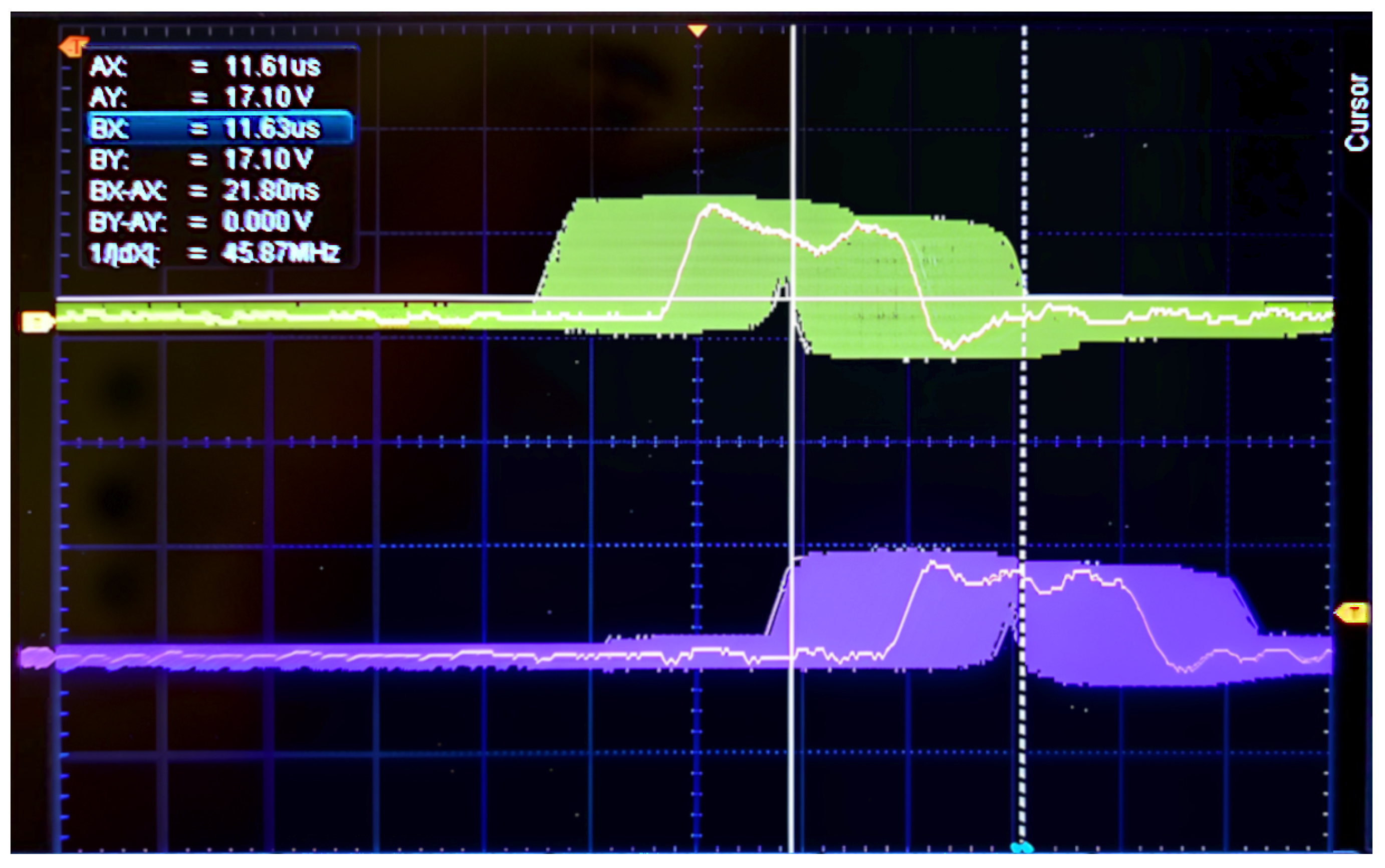
A variant of the model that includes noise sources (i.e., sources of randomness other than initial pulse length) was created in order to better model expected outcomes on real hardware. In this variant, the ideal delays— t d e l 1 , t d e l 2 —were replaced with a cascade of inverter gate models, which resembles the final implementation. The circuit macromodel with noise voltage sources and noise sources’ parameters was adjusted to match the dynamics for both a single logical primitive and the delay lines. Each gate model had a voltage noise source added in series with the gate input, and each source had a unique seed (thus, they were uncorrelated). The authors acquired multiple responses of the circuit; moreover, a jitter of standalone delay lines was subjected to analysis. The estimated voltage variation for noise sources was determined with the help of a looped counter clocked by a local ring oscillator on the device. We obtained noise estimates by examining the deviations in time between start and stop pulse of the counter on an oscilloscope in persistence mode (Figure 8).

2.2. TRNG Implementation in CPLD

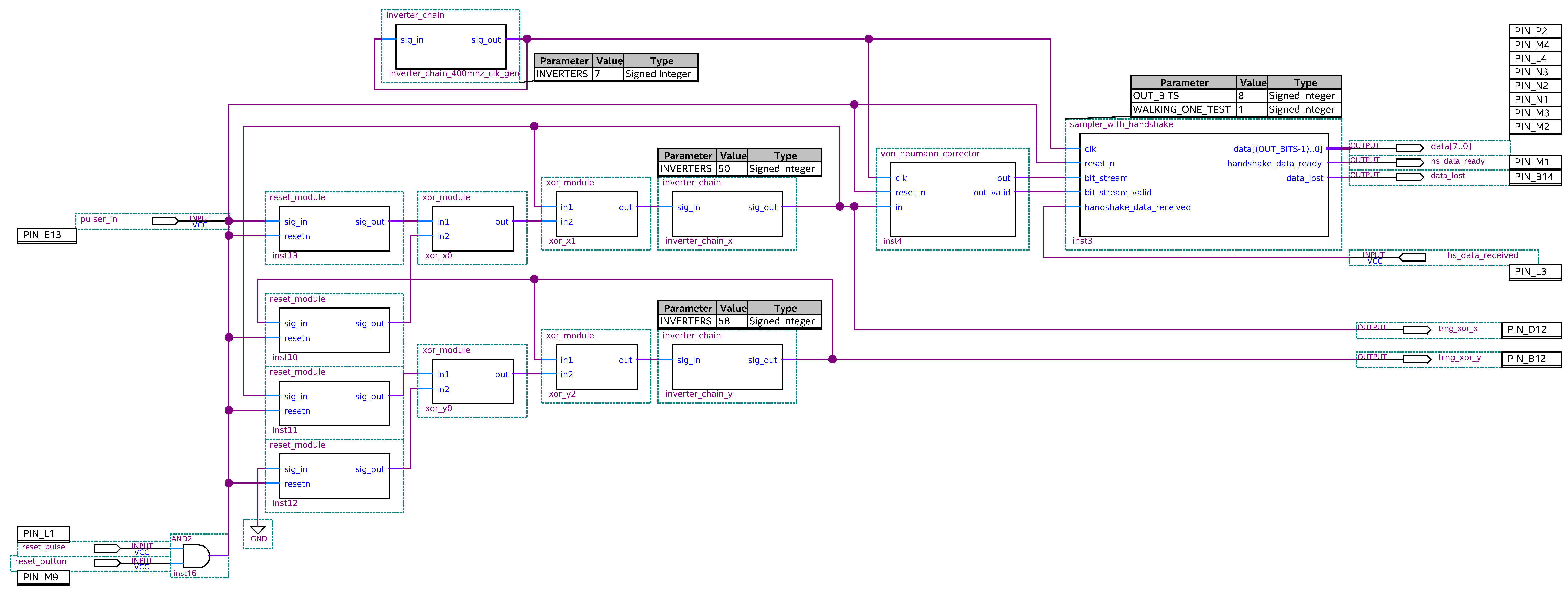
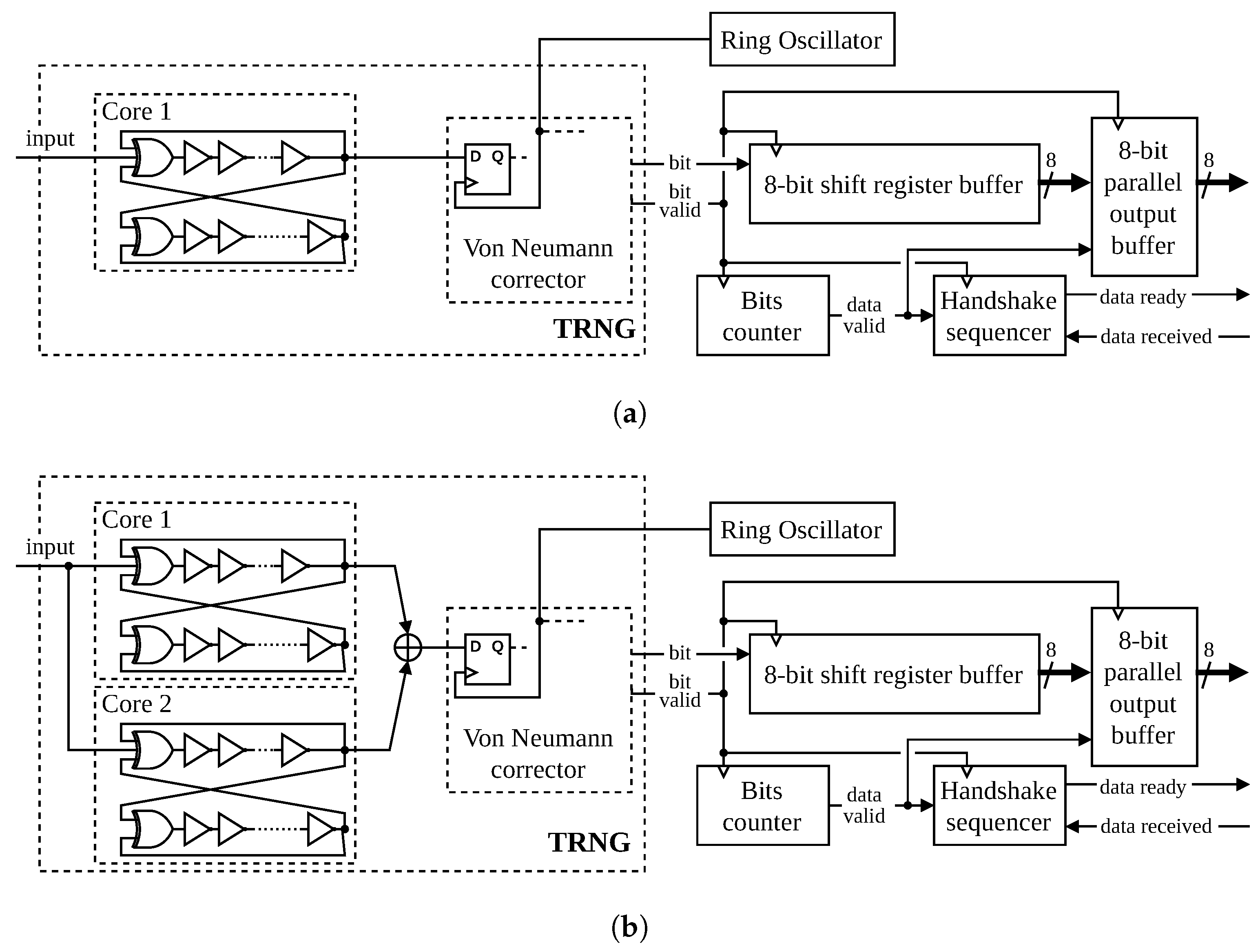
The authors wanted to emphasize the simplicity of the design; therefore, we decided to perform an implementation in a low-resource reconfigurable device, namely the Altera MAX® V 5M570Z CPLD (manufactured by Intel Corporation based in Santa Clara, CA, United States) hosted on the MAX® V Development Kit board. The block design of a single-core TRNG variant is presented in Figure 9. The logic circuits were described using Verilog Hardware Description Language. The XOR gate implementation was straightforward, instantiated simply by applying the XOR operator on the signals. To ensure that XOR gates would not be subject to logic optimization, lcell primitive was used to instantiate them. It is a construct recognized by Quartus® Prime 23.1 software that assigns a dedicated logic cell resource inside the CPLD for specified logic.
The delay paths were implemented as a chain of an even number of inverters. A pair of inverters (connected in series) negates each other’s signal, so x i n = x o u t . However, a propagation delay is introduced. Thus, a certain number of inverter pairs can introduce a certain delay. The inverter_chain block was described as an HDL signal vector using a concurrent, combinatorial statement. Each consecutive bit of the vector is assigned a negated bit from the previous index of the vector. Because logically, the input signal would equal the output signal, the synthesis tools tend to perform optimization to reduce seemingly unnecessary negations and collapse them into a pass-through signal. In order to avoid it, the /* synthesis keep */ attribute was assigned during the declaration of the vector signal. The inverter chain block allowed handy declarations of the delay paths (for an even number of inverters) and ring oscillators (for an odd number of inverters). The resulting circuitry was then inspected in Quartus post-synthesis and post-fitting schematics to make sure that the core logic of the TRNG remained intact. Apart from the previously mentioned measures, all logic-altering optimization options were disabled in synthesis and implementation tools.
Due to practical purposes, the TRNG includes reset functionality (reset_module blocks), allowing the circuit to start from a known state or stop the operation at any moment. If a reset_n signal is active, then outputs of the reset blocks force logical zero; otherwise it is a pass-through for sig_in signal. An additional XOR gate was introduced at the TRNG core’s input for signal path routing. To conserve symmetry between paths, another XOR was added in the second path to adjust the delays and keep propagation conditions the same. We decided that the start and reset pulses would be applied externally, from outside of the CPLD, for a more convenient testing setup. Finally, the outputs of the delay paths were routed to IO buffers so that the resulting waveforms could be inspected with an oscilloscope.
The raw, fast-changing signal at the output of the TRNG core is more analog in its character than digital. Because no clocked, synchronous elements were used in the core’s design, it switches extremely fast. It can be subject to external factors like bandwidth cut-off due to parasitic capacitances, distortions introduced by IO buffers, or noise and interference in the external signal transmission medium. Hence, it was decided that the sampling circuit shall be implemented in the CPLD to capture the core’s raw output bitstream directly in its purest form.
The core output was routed to an I/O with the fastest available standard setup (i.e., 3.3 V LVTTL with the highest drive fan-out) and inspected with an oscilloscope. The shortest interval between upcoming data was roughly 10 ns; therefore, the sampling frequency was set to 200 MHz to satisfy the Nyquist–Shannon criterion. An onboard oscillator had a frequency of only 10 MHz, and the CPLD used has no PLL or any other hardware capable of clock multiplication. Hence, ring oscillators were implemented inside the CPLD to clock the sampler’s circuit.
A short RO order sweep was conducted for lengths of 3, 5, and 7 inverters. The resulting frequencies were 365 MHz, 270 MHz, and 195 MHz, respectively. The output waveforms were not observed directly. They were, however, fed to a clock divider at the output of RO. The divided clock was inspected with an oscilloscope to assess phase and frequency stability. The direct, undivided output of RO was then assigned a clock constraint, with an estimated frequency, so that it could be recognized by the tools as a valid clock and perform the appropriate timing. The relationship between observed clock frequencies for a given number of inverters allowed us to roughly estimate the delay of a single inverter.
The collected bits from the core’s output stream were buffered and organized as parallel data into an 8-bit bus, making the transmission less time-restrictive for the receiving module, which also had to conduct a handshake sequence between received samples. Consequently, eight parallel registers holding the stable output sample had to be appropriately timed by the internal logic and implementation tools, which proved challenging. Hence, the sampler’s circuit has been divided into two, differently clocked parts: one with Von Neumann’s (VN) corrector [39], and another with the bits buffering circuit and handshake sequencer. Due to the extreme simplicity of the implementation of the corrector, it was able to run at clock frequencies up to 243 MHz, as calculated by timing analysis tools. The corrector outputs a bit valid flag after capturing and comparing a pair of bits. When this flag is output, the subsequent logic actually acts. Hence, it was decided that the bit valid signal would be used as a clock for subsequent logic instead of using it as a regular signal. It was done for two reasons. 1. This resulted in loosened timing constraints by half in the bit-buffering part of the circuit. 2. Because the bit valid signal affected almost every cell in the buffering logic, selecting the clock path for its propagation was much more efficient than trying to match the timing of the regular signal and the system clock. This means that if the corrector did not output enough cycles, a byte of data from a burst would be lost, but this was negligible. Corrector outputs data at most every two cycles (only if a differing pair of bits is captured), so the timing constraint was put on the bit valid signal to treat it like a derived clock from the Ring Oscillator with half the frequency. The final clock frequency available for the part of the circuit with buffers was evaluated using timing analysis tools, and it was determined to be 116 MHz. To summarize, the Von Neumann corrector can run at frequencies up to 243 MHz, and the bit-buffering circuit with handshake sequencer at frequencies up to 116 MHz. The minimum sampling frequency was determined to be at least 200 MHz, while the closest available clock frequencies from local ROs were either 270 MHz or 195 MHz. The former was way too fast for the designed logic; the latter was a sufficient compromise.
Due to limitations of the chosen CPLD, finding a logic implementation for the sampling circuit that allowed such frequencies required conducting a sweep of at least 100 fitter seeds (initial value for the tool responsible for assigning synthesized logic to physical hardware and routing it) to obtain a proper working solution. However, it is important to note that it may not be the case for more sophisticated models of CPLDs or FPGAs.
The final diagram for the single-core design can be found in Figure 10a. It can be easily extrapolated to two (Figure 10b) or more cores by duplicating the TRNG core blocks and XORing outputs before the Von Neumann corrector. In Section 3.2.2, we show that the second core was necessary to achieve true randomness. The utilization of resources for each number of cores for the case of delay paths consisting of 50 and 58 inverters (one of the successful test cases that required the least resources) is shown in Table 1.

2.3. Data Acquisition Method

The evaluation board used to receive and acquire parallelized samples was Arty S7-25, hosting a Xilinx XC7S25-CSGA324 FPGA (Spartan-7 family, manufactured by Advanced Micro Devices, Inc. based in Santa Clara, CA, USA). The FPGA board is wired together with the MAX V CPLD board to allow data transmission using the designed interface. When a byte of data is sent by the CPLD, both devices conduct a handshake to make sure the sample is stable. After the handshake is complete, the received byte of data is buffered inside a FIFO of 8192 depth and sent via UART at a baud rate of 4 Mbps to a PC. To further speed up data collection, a timeout was implemented that sends the delimiter sequence to the PC if no new data appears for a specified amount of time. The timeout was also used to estimate throughput, which in our case was calculated as an average number of output bytes per duration of autonomous operation of the core (excluding idle periods) for a total of 10 MB of bursts. For this, the timeout would be triggered not by lack of new data, but by lack of changes directly at the TRNG output from the CPLD board. An additional Python 3.10.12 script collected the incoming data on the PC and saved each burst separately to a file for further analysis. Final setup can be found in Figure 11.

3. Results

3.1. Numerical Analysis

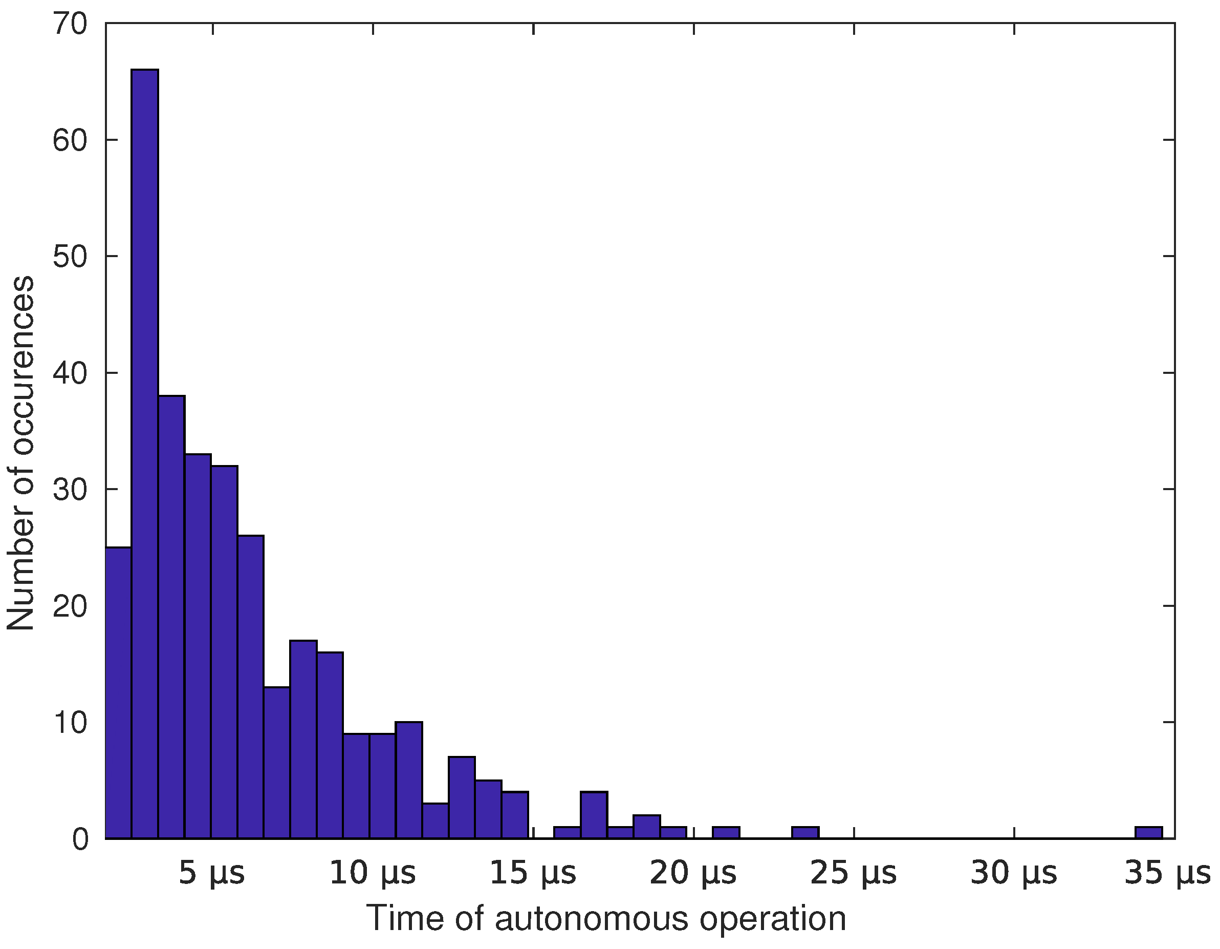
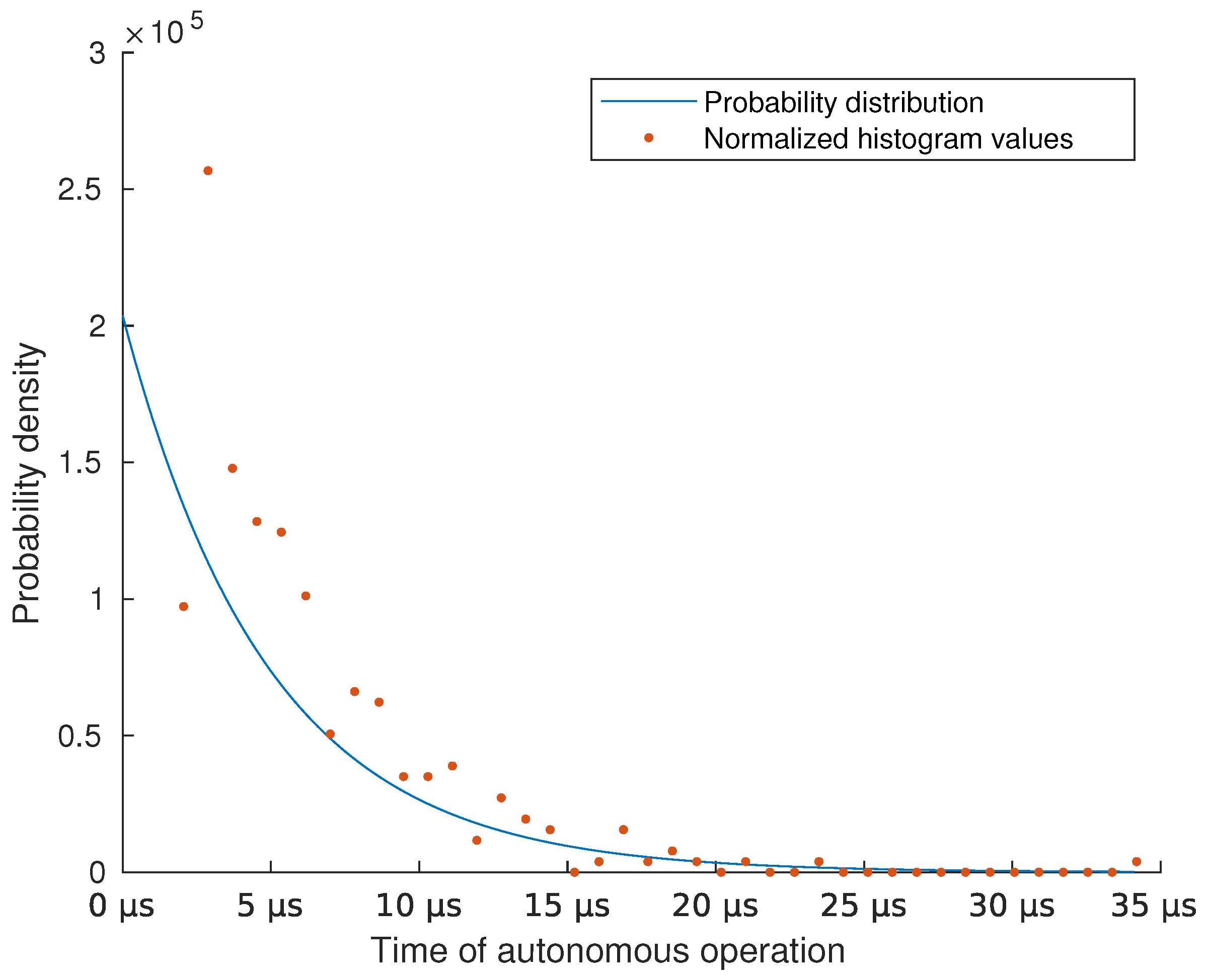
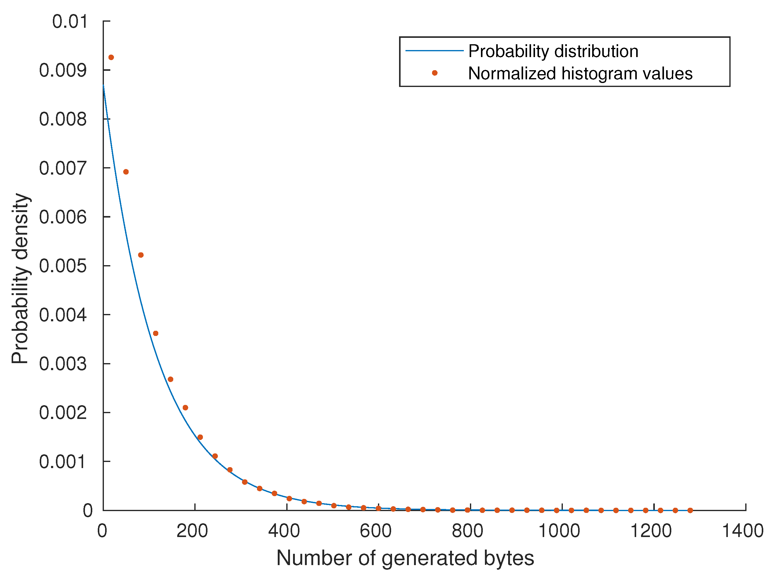
The core macromodel produces deterministic results. Therefore, we added noise sources to the input of each logical primitive. The macromodel of the circuit that includes gate models with noise sources was run for over 300 simulations. The obtained distribution can be seen in Figure 12 and was approximated with an exponential distribution in Figure 13. The λ ^ parameter value of the distribution was estimated to be λ ^ = 203,730. An exponential shape of this histogram indicates an exponential distribution (a special case of the gamma distribution) of t a u t . This means that the core has equal halting probability at any moment of autonomous operation. This also means that, in contrast to a deterministic macromodel of the system described with (1), the noise sources available in the core can affect the momentary circuit trajectory to such an extent that a circuit can stop at any t < t a u t . This indicates a chaotic operation of the system and its memoryless property. The λ ^ distribution parameter can now be used to estimate the circuit’s expected time of autonomous operation E ( t a u t ) (and at the same time its standard deviation), which is 1 / λ ^ = 4.908 μs.
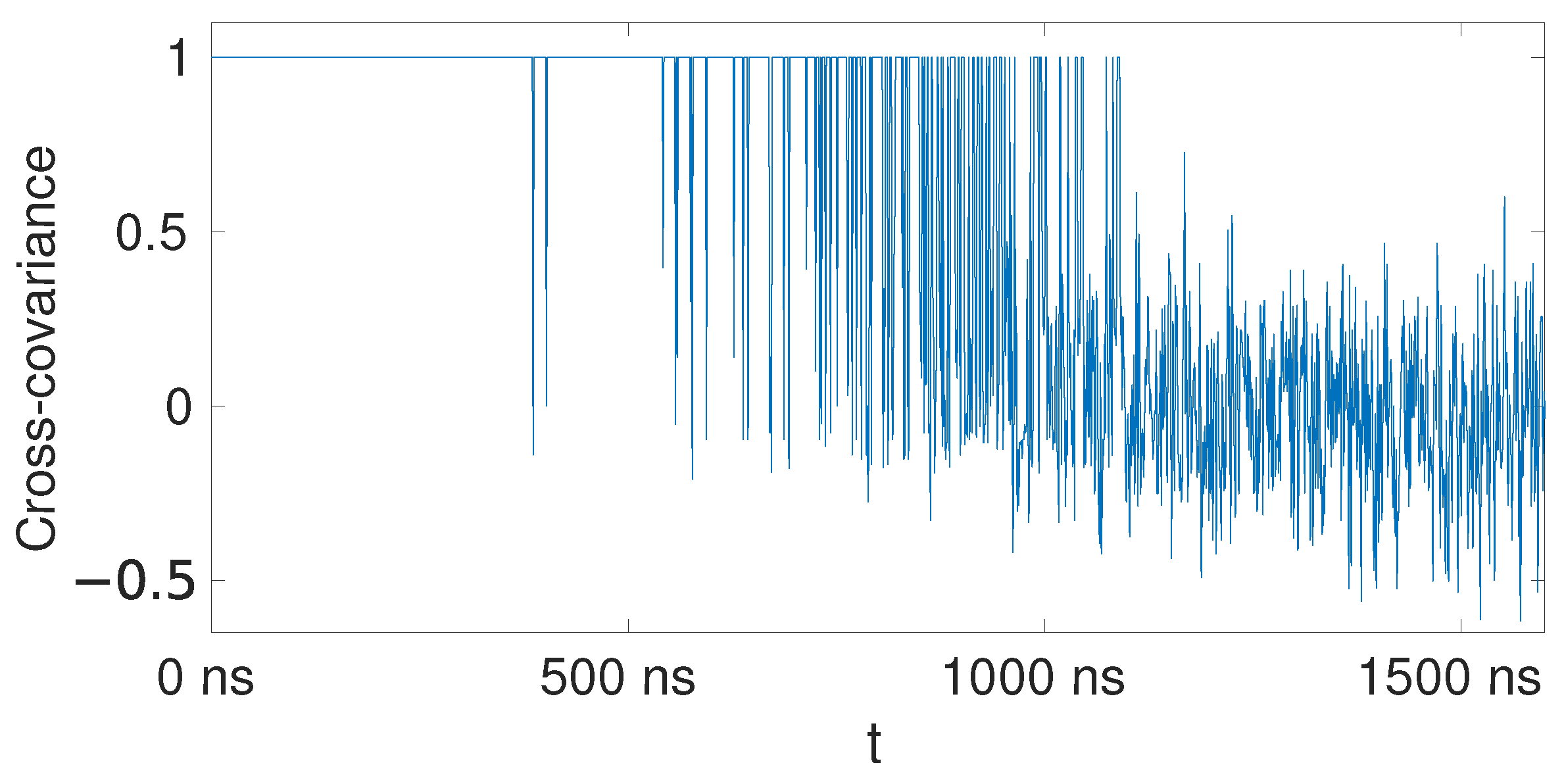
We have also analyzed the cross-covariance for QD output in 40 independent runs (Figure 14). Moreover, a plot of binary logical states in time for this output to visually inspect the divergence of output values between runs is available in Figure 15. Initially, the outputs have very high covariance that tends to oscillate around zero after the core’s warm-up time (circa 1 μs for depicted examples). Despite the presence of warm-up time for the single core, it is later shown that with our post-processing methods, it is irrelevant and negligible in randomness tests for long sequences of numbers concatenated from multiple bursts.

3.2. Empirical Verification

3.2.1. Single Core Performance

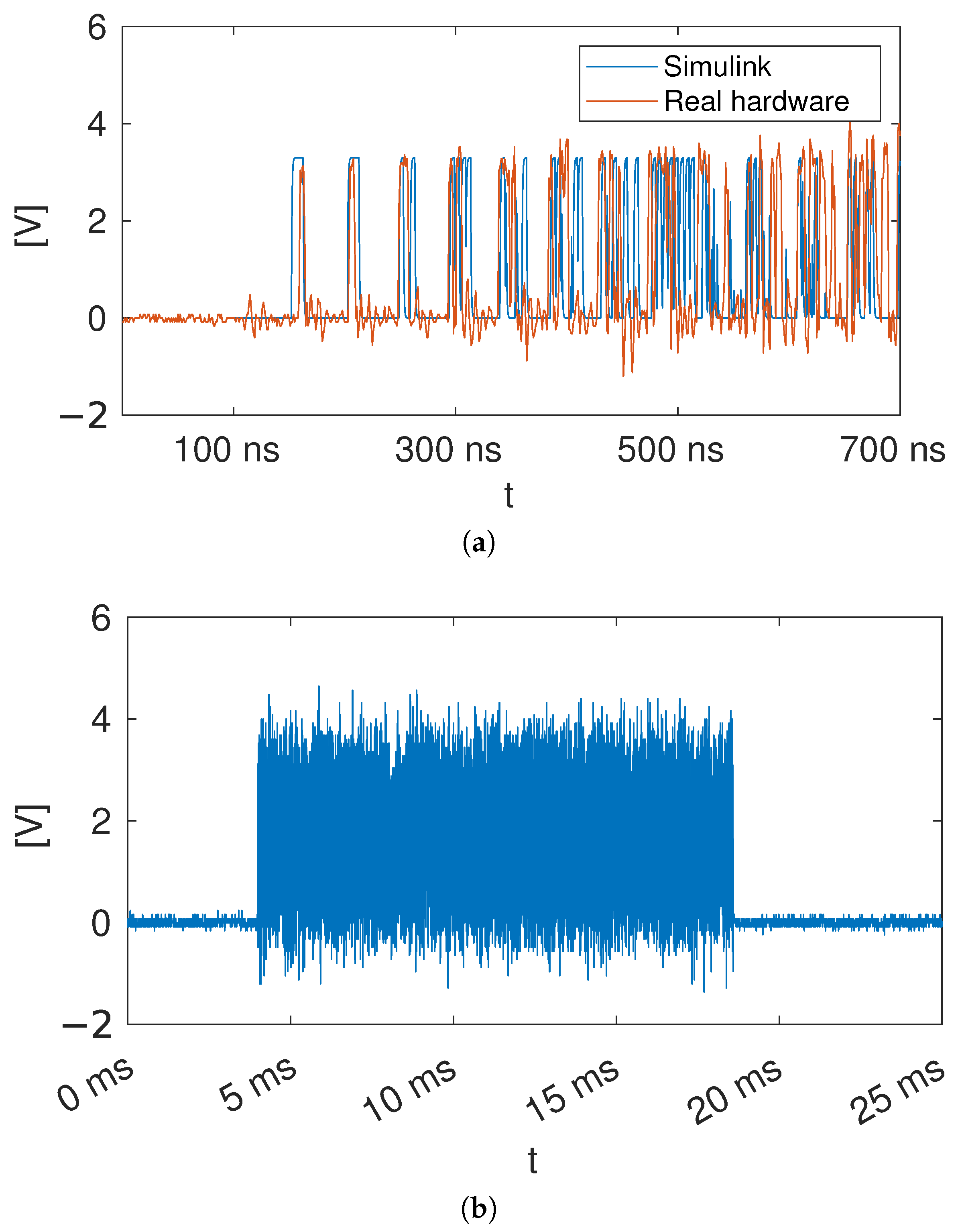
First, the behavior of a single TRNG core with the VN corrector was inspected. We started by capturing raw core outputs with an oscilloscope (Figure 16) and concluded that the implementation matches its behavior with the model. Next, we analyzed the final sample values returned by the TRNG. In Figure 17 we have put burst length distributions (measured in number of 8-bit output samples) for three different implementation cases. Figure 18 contains greyscale representations of collected data. In Figure 19 the single best burst histograms are displayed, while in Figure 20 are the histograms of all the collected data for a given case. We have found that burst length distributions (measured in number of 8-bit output samples) were varying for various fitter seeds and various delay path lengths, as can be seen in Figure 17, whereas the exponential distribution in Figure 17b matched the one obtained in Section 3.1. Its λ ^ parameter was determined to be 0.0087; thus, the expected burst length in bytes for this case is 114. The resulting probability density distribution plot has been put in Figure 21. The following delay path lengths (measured in number of inverters) were tested for QD and PD, respectively: (10, 12); (50, 58); (100, 110). The results for (10, 12) were suboptimal and TRNG generated only a few bits within a burst and stopped. The expected number of generated samples was not constant per delay length and varied with different fitter seeds, as can be seen by comparing Figure 17a,b. We did not put any constraints on the placement of the TRNG core. It was routed and placed automatically by the tools, which may be considered a desired circuit property.
When all the collected numbers for each case are concatenated and plotted as a greyscale picture, there is no obvious pattern for the different distribution cases. However, when histograms of samples for single best runs (by the merit of the χ 2 test) and all the runs together are inspected, it is clear that the distributions do not adequately resemble a desired uniform distribution, so they do not qualify for the NIST tests. For this reason, the TRNG was extended to two cores. To conclude, the differences between greyscale pictures and single-burst value distributions for cases (a)–(c) are very subtle, and the overall shapes of burst length distributions may differ, but do not seem to affect the system’s performance for large data sets. Generally, the circuit is not sensitive to the placement of the elements inside the CPLD (which was manipulated by setting up the fitter’s seed) and does not require manual routing. However, in some cases, due to variations of propagation times between nodes inside CPLD, it may result in a solution having slightly less favorable final delay path times (which is shown in Figure 4). This effect was negligible in a dual-core setup.

3.2.2. Dual Core Performance

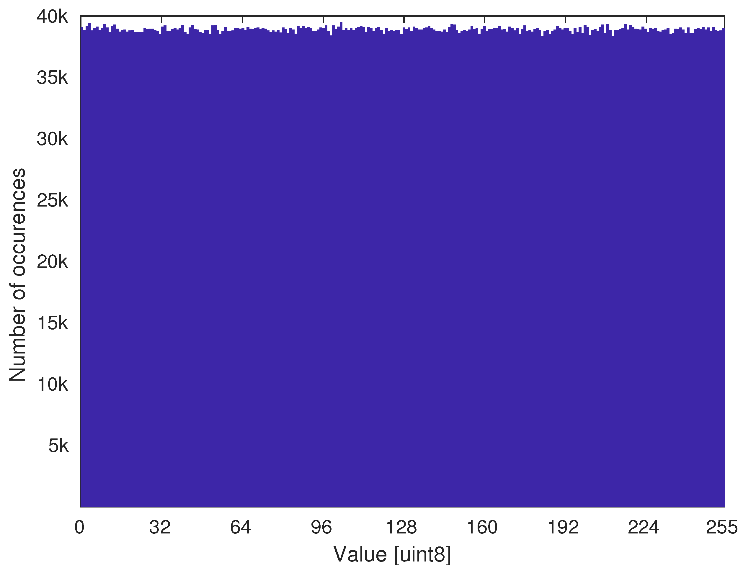
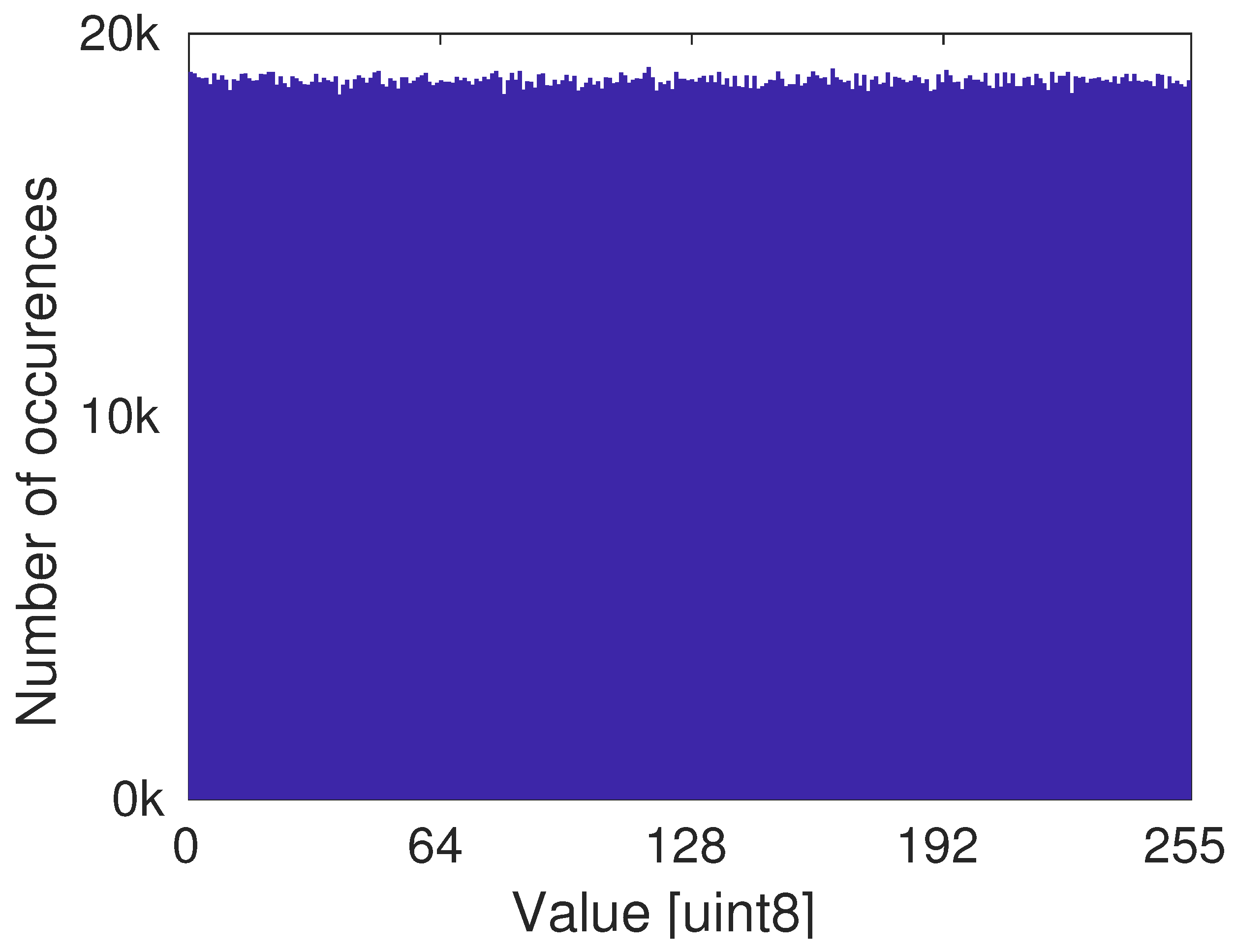
By extending the TRNG design to two cores (Figure 10b), we managed to obtain an excellent uniform distribution (Figure 22) and performance in randomness tests. Comparison with the most recent TRNG designs in Table 2 shows that our work achieves satisfactory throughput, considering the resources utilized and low power consumption (which was estimated using Altera’s Early Power Estimators). It is competitive regarding resource utilization for TRNGs that use chaos as an entropy source and implemented fully on programmable logic devices. When compared against other TRNGs, it falls short. However:
  • It is important to note that the majority of LUTs are consumed for delay paths, and the circuit was not optimized in terms of resources used. We focused on properly operating designs according to the macromodel.
  • Throughput had to be reduced due to limitations of the platform. Sampling speed had to be slow enough to allow the sampler and transmitter logic to work. The VN corrector itself reduces the transmission rate by at least half. Up to a certain point, there is an interchangeability between sampling speed and number of cores; however, the limitation is burst length—more intense decimation results in lower burst lengths (measured in number of output bits).
  • Our design can work on most low-resource platforms—no specialized hardware resources are necessary.

3.2.3. Concept Validation with an FPGA

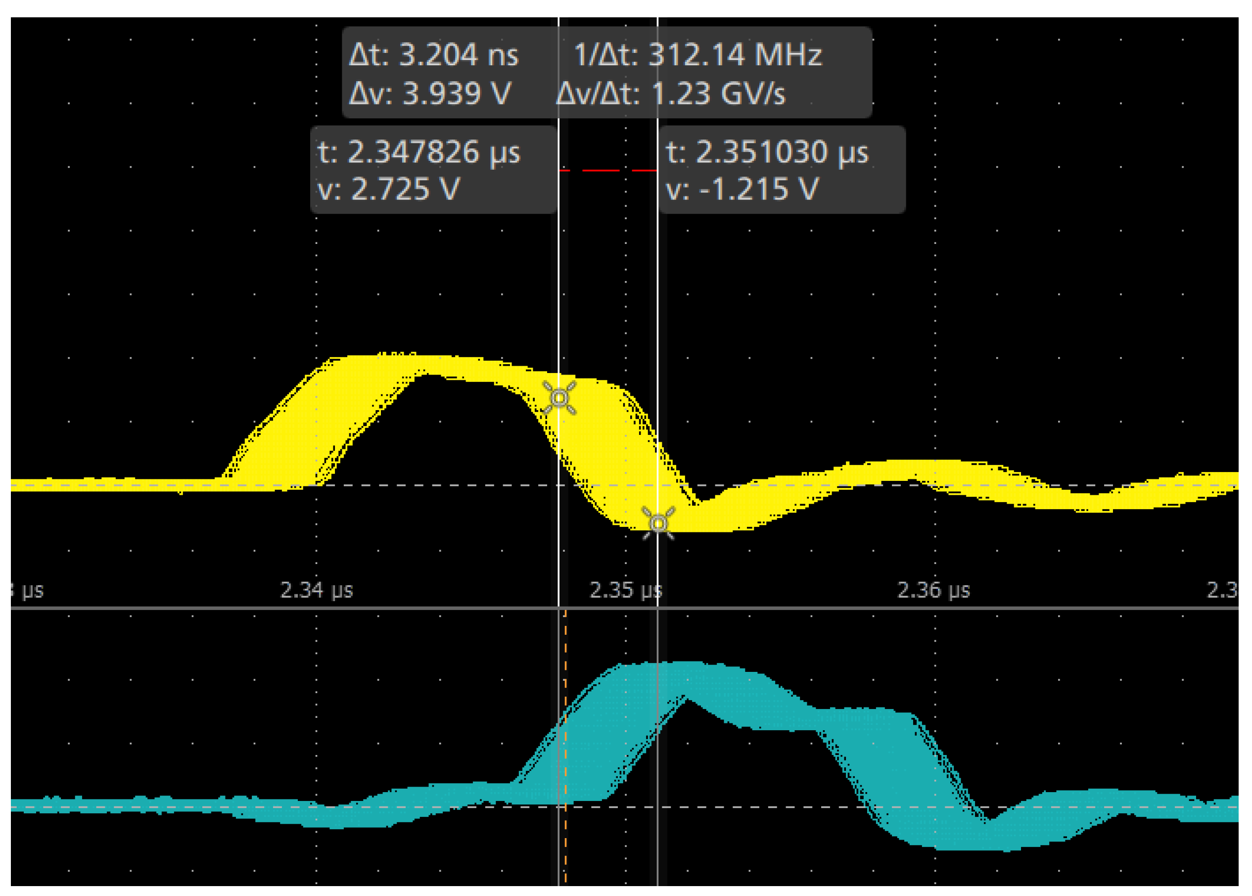
The TRNG was implemented on a modern Spartan-7 FPGA for a brief comparison. The FPGA used was the same Xilinx XC7S25-CSGA324 from the previous CPLD test and acquisition setup. For comparison purposes, the jitter was measured using a similar method as for the CPLD (Figure 23), and it was determined to be 27% lower than that of the CPLD, while the switching frequency was approximately 5 times higher.
The presence of noise sources that cause the jitter is mandatory for the proper operation of this TRNG. Therefore, we expected that the FPGA implementation would also yield an exponential distribution of the autonomous operation time, manifesting the same stochastic process previously observed in the CPLD. The phenomena exploited in this TRNG are scalable with frequency. The measurements proved this right, as shown in Figure 24. One can see that this is the same process as the one modelled by the macromodel and the one used in the CPLD. The main difference was the lower jitter, which results in lower entropy for the single core. Sure enough, only after extending the design to four cores (compared to a double-core TRNG in the CPLD) did we obtain a uniform distribution of output samples (Figure 25) suitable for the generation of truly random numbers. Another important observation is that for the same number of inverters in delay chains, i.e., 50 and 58, the FPGA implementation had a longer autonomous operation time than that of the CPLD implementation. This can be easily explained by the higher bandwidth of the circuit, the consequences of which were described in Section 1.2. A lower RC constant of individual gates results from a more precise fabrication process for this modern FPGA, compared to the CPLD [40].
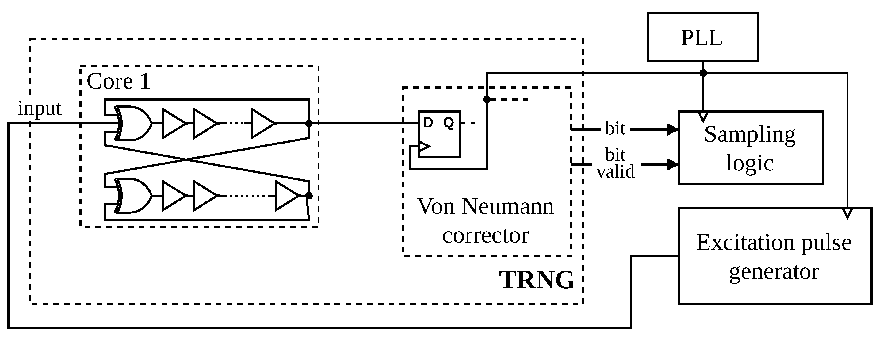
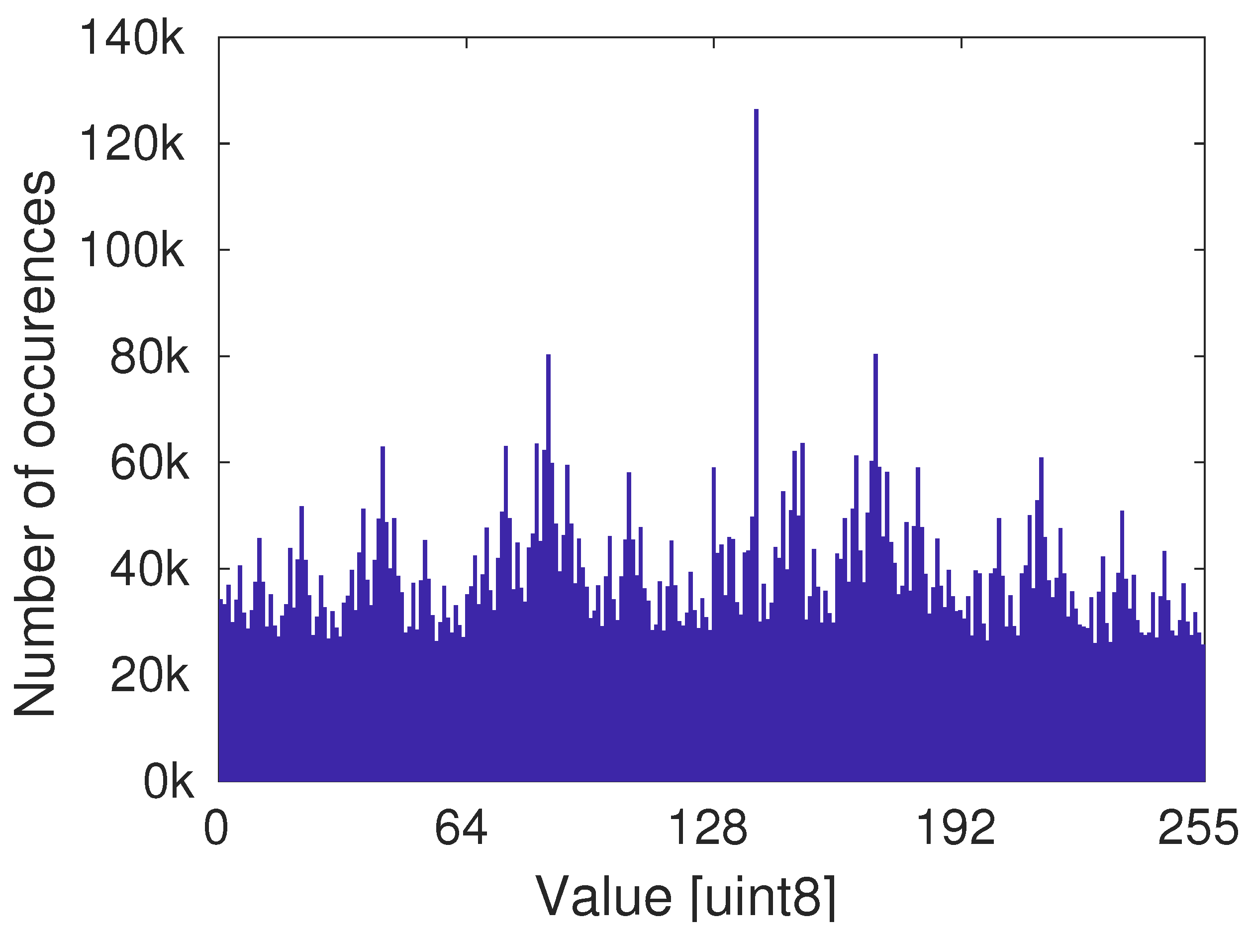
The FPGA implementation could take advantage of a 200 MHz PLL clock for the logic of the VN corrector and the TRNG sampler. The same clock was also used for the logic that outputs an excitation pulse for the TRNG (Figure 26). This resulted in a more synchronous design compared to the CPLD-FPGA setup. The generation of the excitation pulse and the moments of sampling of the core’s raw output stream were in significantly more regular time intervals. Consequently, the number of occurrences of TRNG’s warm-up bytes in FPGA implementation was overrepresented, as is visible in Figure 27. The byte with a value of 139 appears more frequently than others. Thus, the first byte from each burst had to be truncated. In this clocking setup, the throughput was higher, but roughly at the same level as that of the CPLD, i.e., around 48 Mb/s on average.

3.3. Statistical Tests

We have examined the dual-core TRNG bitstream from the CPLD using NIST SP 800-22 batteries of tests [5] supplied by National Institute of Standards and Technology based in Gaithersburg, MD, United States. NIST tests are a standard method of evaluating large data sets for their randomness. The bitstream can be considered truly random if all the NIST tests are passed. We tested 154 sequences of 1 Mbit length from almost 20 MB of data obtained by concatenating multiple bursts. The result of each sequence test is a p-value. We chose α = 0.01 level of significance. A test is considered as passed if p-value > α . The results and pass rates were put together in Table 3.
Similarly to [41], if the test has multiple variants, we also conduct second-level tests that examine the results themselves—true randomness should exhibit uniform distribution of p-values, thus proving global randomness of the results. For this purpose, we employ the Kolmogorov–Smirnov ( K S ) test to check for the uniformity of results in case of small batches and the chi-squared ( χ 2 ) test to check for the uniformity of results but over bins of p-values. The results evaluated in this manner are marked accordingly in the table.
All the NIST tests were passed, with the worst p-value (for non-uniformity tests) of 0.1125 and the worst pass rate of 0.9679. This affirms that our TRNG produces truly random sequences of numbers.

4. Discussion

The TRNG macromodel predicts the behavior of both CPLD and FPGA implementations adequately. The main differences are the jitter and RC constants of individual gates, which affect the average time of autonomous operation and entropy of a single core. Despite different switching rates of hardware on the CPLD and the FPGA, the final throughput for 200 MHz sampling clocks (a slightly lower value for the CPLD due to the RO used for clock generation, and almost the exact value for the FPGA due to the PLL) in both implementations was similar—circa 44–48 Mb/s. Thus, the throughput can be increased by increasing the sampling frequency. However, it remains a matter for further investigation how densely the raw output stream can be sampled. As the FPGA has a higher switching rate, one can conclude that more dense sampling may be applicable without loss of quality of randomness, but it was not verified in the scope of this paper. Conversely, reducing the sampling rate may actually lead to the TRNG with a single core having sufficient performance to pass randomness tests. Adding more cores to a single TRNG was simply a countermeasure to increase entropy for the current high-sampling-rate setup. Beyond a specific sampling, the TRNG does not benefit from an increased number of cores as sufficient entropy is reached. On the other hand, a higher throughput for the current setup and performance can be obtained by parallelizing multiple TRNGs.
A warm-up of the TRNG proved to be more problematic in the FPGA implementation due to its synchronous nature. To avoid this issue, a free-running ring oscillator is recommended to clock the VN corrector. This would allow more random sampling of the initial raw output stream (due to asynchronous excitation pulse), thus decreasing occurrences of similar warm-up bytes, which was the case for the CPLD. This may also increase the entropy of the TRNG in a way that would allow the FPGA implementation to reduce the number of cores, similar to the CPLD one. Another applicable countermeasure is rejection of the initial byte from the output stream.
The TRNG operates in bursts, a feature which can be investigated in future works for applicability in combined TRNG and Physically Unclonable Function (PUF) designs. PUFs are another scope of application that may enable unique device identification by measuring the bursts’ properties of individual devices. These properties should be unique for each instance due to fabrication process mismatches. The TRNG can be forced to operate constantly without idle periods by application of an excitation pulse at constant time intervals adjusted to the most common t a u t in a given distribution. The randomness properties of such a mode were not investigated and they may be slightly different due to overlapping of adjacent bursts.

5. Conclusions

We have proposed a simple and relatively compact TRNG design that takes advantage of multiple sources of entropy, i.e., randomness of the initial solution (the length of the starting pulse) and the noise of gates in a delay chain. It exploits elementary digital logic components and can be implemented on a very resource-deprived platform like the CPLD. The implementation did not require either specialized hardware primitives, like PLLs, DCMs, arithmetic and signal-processing blocks, carry-chains, or even a stable source of clock signal. We have examined the TRNG core macromodel and hardware implementations, and successfully tested the dual-core design for true randomness using the NIST test battery.
The measurements that were carried out proved the validity of the derived macromodel. Similar outcomes and distribution as in the stochastic simulation were observed for both the CPLD and FPGA implementations. Despite different switching rates for both devices (as per jitter estimation measurements), the TRNG operating principle remained valid, thus showing that the phenomena scale with frequency.
A single-core TRNG was insufficient to obtain truly random numbers at the output as assessed with the NIST test suite. Depending on the strength of noise (jitter) sources present in the hardware, a certain number of cores was required to reach sufficient entropy for a uniform distribution of values at the output of the TRNG: two for the CPLD and four for the FPGA. There is also a possible tradeoff between the sampling rate of the TRNG core’s raw output stream (which limits the throughput) and the number of necessary cores (which increases resource utilization) to reach high enough entropy for producing truly random numbers.
Overall, low complexity, resource utilization, and power consumption put this design up as a suitable candidate for IoT devices. There is also space for further exploration of potential applications of this TRNG. For example, its burst-mode operation may potentially be used in a unified design that combines TRNG and PUF.

Author Contributions

Conceptualization, P.Z.W.; methodology, B.M.S. and P.Z.W.; software, B.M.S.; validation, B.M.S. and P.Z.W.; formal analysis, P.Z.W.; investigation, P.Z.W. and B.M.S.; resources, P.Z.W. and B.M.S.; data curation, P.Z.W. and B.M.S.; writing—original draft preparation, B.M.S.; writing—review and editing, B.M.S. and P.Z.W.; visualization, P.Z.W. and B.M.S.; supervision, P.Z.W.; project administration, P.Z.W.; funding acquisition, n/a. All authors have read and agreed to the published version of the manuscript.

Funding

Statutory Funds of Institute of Electronic Systems.

Data Availability Statement

Data is contained within the article.

Conflicts of Interest

The authors declare no conflicts of interest.

References

  1. Goldberg, I.; Wagner, D. Randomness and the netscape browser. Dr. Dobb’s J. 1996. [Google Scholar]
  2. Peterson, I. Lava Lamp Randomness. Available online: https://www.sciencenews.org/article/lava-lamp-randomness (accessed on 1 September 2025).
  3. Hofemeier, G.H. What is Intel® Secure Key Technology? Available online: https://www.intel.com/content/www/us/en/developer/articles/technical/what-is-secure-key-technology.html (accessed on 1 September 2025).
  4. Taylor, G.; Cox, G. Behind Intel’s new random-number generator. IEEE Spectrum, 2 December 2021; pp. 1–9. [Google Scholar]
  5. Bassham, L.E.; Rukhin, A.L.; Soto, J.; Nechvatal, J.R.; Smid, M.E.; Barker, E.B.; Leigh, S.D.; Levenson, M.; Vangel, M.; Banks, D.L.; et al. SP 800-22 Rev. 1a. A Statistical Test Suite for Random and Pseudorandom Number Generators for Cryptographic Applications; Technical Report; National Institute of Standards & Technology: Gaithersburg, MD, USA, 2010. [Google Scholar]
  6. Safi, M.; Simpson, B.; Clark, E.; Idriss, H.; Idriss, T. Lightweight Random Obfuscation Protocol: A PUF-based Mutual Authentication Protocol for IoT Devices. In Proceedings of the 2023 IEEE International Conference on Artificial Intelligence, Blockchain, and Internet of Things (AIBThings), Mount Pleasant, MI, USA, 16–17 September 2023; pp. 1–5. [Google Scholar] [CrossRef]
  7. Kok, C.L.; Ho, C.K.; Lee, T.K.; Loo, Z.Y.; Koh, Y.Y.; Chai, J.P. A Novel and Low-Cost Cloud-Enabled IoT Integration for Sustainable Remote Intravenous Therapy Management. Electronics 2024, 13, 1801. [Google Scholar] [CrossRef]
  8. Cui, J.; Yi, M.; Cao, D.; Yao, L.; Wang, X.; Liang, H.; Huang, Z.; Qi, H.; Ni, T.; Lu, Y. Design of True Random Number Generator Based on Multi-Stage Feedback Ring Oscillator. IEEE Trans. Circuits Syst. II Express Briefs 2022, 69, 1752–1756. [Google Scholar] [CrossRef]
  9. Bharat Meitei, H.; Kumar, M. Design and Implementation of Multiple Ring Oscillator-Based TRNG Architecture by Using ADPLL. IEEE Access 2025, 13, 9252–9264. [Google Scholar] [CrossRef]
  10. Della Sala, R.; Bellizia, D.; Scotti, G. Unveiling the True Power of the Latched Ring Oscillator for a Unified PUF and TRNG Architecture. IEEE Trans. Very Large Scale Integr. (VLSI) Systems 2024, 32, 2403–2407. [Google Scholar] [CrossRef]
  11. Ahmed, H.O.; Kim, D.; Buchanan, W.J. A True Random Number Generator Based on Race Hazard and Jitter of Braided and Cross-Coupled Logic Gates Using FPGA. IEEE Access 2024, 12, 182943–182955. [Google Scholar] [CrossRef]
  12. Wang, X.; Liang, H.; Wang, Y.; Yao, L.; Guo, Y.; Yi, M.; Huang, Z.; Qi, H.; Lu, Y. High-Throughput Portable True Random Number Generator Based on Jitter-Latch Structure. IEEE Trans. Circuits Syst. I Regul. Pap. 2021, 68, 741–750. [Google Scholar] [CrossRef]
  13. Liu, Y.; Wu, Y.; Chen, B.; Sang, P.; Wu, J.; Wei, X.; Zhan, X.; Chen, J. High-Speed True Random Number Generator with Multiple Entropy Sources: Ring Oscillator Jitter and Random Telegraph Noise. IEEE Embed. Syst. Lett. 2025, 1. [Google Scholar] [CrossRef]
  14. Rajski, J.; Trawka, M.; Tyszer, J.; Włodarczak, B. A Lightweight True Random Number Generator for Root of Trust Applications. IEEE Trans. Comput. Aided Des. Integr. Circuits Syst. 2023, 42, 2815–2825. [Google Scholar] [CrossRef]
  15. Della Sala, R.; Bellizia, D.; Scotti, G. High-Throughput FPGA-Compatible TRNG Architecture Exploiting Multistimuli Metastable Cells. IEEE Trans. Circuits Syst. I Regul. Pap. 2022, 69, 4886–4897. [Google Scholar] [CrossRef]
  16. Chen, C.; Li, S.; Song, C. A 200 kb/s 36 µw True Random Number Generator Based on Dual Oscillators for IOT Security Application. Electronics 2023, 12, 2332. [Google Scholar] [CrossRef]
  17. Mahalingam, H.; Rethinam, S.; Janakiraman, S.; Rengarajan, A. Non-Identical Inverter Rings as an Entropy Source: NIST-90B-Verified TRNG Architecture on FPGAs for IoT Device Integrity. Mathematics 2023, 11, 1049. [Google Scholar] [CrossRef]
  18. Matuszewski, Ł.; Jessa, M. A Low-Complexity Start–Stop True Random Number Generator for FPGAs. Appl. Sci. 2024, 14, 5642. [Google Scholar] [CrossRef]
  19. Frustaci, F.; Spagnolo, F.; Corsonello, P.; Perri, S. A High-Speed and Low-Power DSP-Based TRNG for FPGA Implementations. IEEE Trans. Circuits Syst. II Express Briefs 2024, 71, 4964–4968. [Google Scholar] [CrossRef]
  20. Cao, Y.; Liu, W.; Zheng, Y.; Chen, S.; Ye, J.; Qian, L.; Chang, C.H. A New Reconfigurable True Random Number Generator and Physical Unclonable Function Unified Chip with On-Chip Auto-Calibration. IEEE Trans. Circuits Syst. I Regul. Pap. 2023, 70, 4900–4913. [Google Scholar] [CrossRef]
  21. Ni, T.; Peng, Q.; Bian, J.; Yao, L.; Huang, Z.; Yan, A.; Wang, S.; Wen, X. Design of True Random Number Generator Based on Multi-Ring Convergence Oscillator Using Short Pulse Enhanced Randomness. IEEE Trans. Circuits Syst. I Regul. Pap. 2023, 70, 5074–5085. [Google Scholar] [CrossRef]
  22. Guan, Z.; Liu, M.; Xu, J.; Lin, C. A hybrid entropy source scheme for true random number generator. Integration 2025, 104, 102473. [Google Scholar] [CrossRef]
  23. Grujić, M.; Verbauwhede, I. TROT: A Three-Edge Ring Oscillator Based True Random Number Generator with Time-to-Digital Conversion. IEEE Trans. Circuits Syst. I Regul. Pap. 2022, 69, 2435–2448. [Google Scholar] [CrossRef]
  24. Wang, J.; Huang, Z.; Chen, Y.; Liu, J.; Zhou, L.; Jiang, X.; Zhou, J.; Wang, Q. An Ultrahigh-Throughput and FPGA-Compatible TRNG Based on Dynamic Hybrid Metastability and Jitter Entropy Cells. IEEE Trans. Circuits Syst. I Regul. Pap. 2025, 72, 2202–2215. [Google Scholar] [CrossRef]
  25. Frustaci, F.; Spagnolo, F.; Perri, S.; Corsonello, P. A High-Speed FPGA-Based True Random Number Generator Using Metastability With Clock Managers. IEEE Trans. Circuits Syst. II Express Briefs 2023, 70, 756–760. [Google Scholar] [CrossRef]
  26. Yang, S.; Liang, H.; Hu, R.; Yao, L.; Huang, Z.; Yi, M.; Lu, Y. Lightweight Hybrid Entropy Source True Random Number Generator Based on Jitter and Metastability. IEEE Trans. Circuits Syst. II Express Briefs 2024, 71, 3513–3517. [Google Scholar] [CrossRef]
  27. Gołofit, K.; Wieczorek, P.Z.; Pilarz, M. A chaos-metastability TRNG for natively flexible IGZO circuits. AEU Int. J. Electron. Commun. 2023, 170, 154835. [Google Scholar] [CrossRef]
  28. Lu, Y.; Cao, C.; Liu, Y.; Liang, H.; Yao, L.; Ma, L. High throughput true random number generator based on dynamically superimposed hybrid entropy sources. Integration 2025, 102, 102380. [Google Scholar] [CrossRef]
  29. Liao, T.L.; Wan, P.Y.; Yan, J.J. Design and Synchronization of Chaos-Based True Random Number Generators and Its FPGA Implementation. IEEE Access 2022, 10, 8279–8286. [Google Scholar] [CrossRef]
  30. Vaidyanathan, S.; Sambas, A.; Abd-El-Atty, B.; El-Latif, A.A.A.; Tlelo-Cuautle, E.; Guillén-Fernández, O.; Mamat, M.; Mohamed, M.A.; Alçin, M.; Tuna, M.; et al. A 5-D Multi-Stable Hyperchaotic Two-Disk Dynamo System With No Equilibrium Point: Circuit Design, FPGA Realization and Applications to TRNGs and Image Encryption. IEEE Access 2021, 9, 81352–81369. [Google Scholar] [CrossRef]
  31. Yuan, F.; Li, S.; Deng, Y.; Li, Y.; Chen, G. Cu-Doped TiO2-x Nanoscale Memristive Applications in Chaotic Circuit and True Random Number Generator. IEEE Trans. Ind. Electron. 2023, 70, 4120–4127. [Google Scholar] [CrossRef]
  32. Paul, P.S.; Sadia, M.; Hossain, M.R.; Muldrey, B.; Hasan, M.S. Cascading CMOS-Based Chaotic Maps for Improved Performance and Its Application in Efficient RNG Design. IEEE Access 2022, 10, 33758–33770. [Google Scholar] [CrossRef]
  33. Wu, H.; Yin, Z.; Xie, J.; Ding, P.; Liu, P.; Song, H.; Chen, X.; Xu, S.; Liu, W.; Zhang, Y. Design and implementation of true random number generators based on semiconductor superlattice chaos. Microelectron. J. 2021, 114, 105119. [Google Scholar] [CrossRef]
  34. Magfirawaty, M.; Lestari, A.A.; Nurwa, A.R.A.; MT, S.; Ramli, K. A Novel Discrete-Time Chaos-Function-Based Random-Number Generator: Design and Variability Analysis. Symmetry 2022, 14, 2122. [Google Scholar] [CrossRef]
  35. Koyuncu, I.; Ozcerit, A.T.; Pehlivan, I. Implementation of FPGA-based real time novel chaotic oscillator. Nonlinear Dyn. 2014, 77, 49–59. [Google Scholar] [CrossRef]
  36. Taki, T. Approximation of junction field-effect transistor characteristics by a hyperbolic function. IEEE J. Solid-State Circuits 1978, 13, 724–726. [Google Scholar] [CrossRef]
  37. Wieczorek, P.Z.; Opalski, L.J. Non-linear modelling of resolve time in D-latch circuits. In Proceedings of the 18th International Conference Mixed Design of Integrated Circuits and Systems—MIXDES 2011, Gliwice, Poland, 16–18 June 2011; pp. 456–459. [Google Scholar]
  38. Wieczorek, P.Z.; Gołofit, K. True Random Number Generator Based on Flip-Flop Resolve Time Instability Boosted by Random Chaotic Source. IEEE Trans. Circuits Syst. I Regul. Pap. 2018, 65, 1279–1292. [Google Scholar] [CrossRef]
  39. Naccache, D. von Neumann Correction. In Encyclopedia of Cryptography, Security and Privacy; Jajodia, S., Samarati, P., Yung, M., Eds.; Springer Nature: Cham, Switzerland, 2025; p. 2742. [Google Scholar] [CrossRef]
  40. Spartan-7 FPGAs Data Sheet: DC and AC Switching Characteristics; Release Date: 18 October 2024; AMD/Xilinx: Santa Clara, CA, USA, 2024; Data Sheet DS189, Revision 1.11.
  41. Wieczorek, P.Z.; Gołofit, K. Dual-Metastability Time-Competitive True Random Number Generator. IEEE Trans. Circuits Syst. I Regul. Pap. 2014, 61, 134–145. [Google Scholar] [CrossRef]
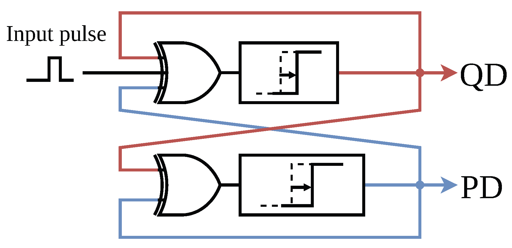
Figure 1. Diagram of the proposed TRNG core.
Electronics 14 03803 g001
Figure 2. Circuit macromodel for t 0 , t p u l s e (a) and (b) for t > t p u l s e .
Electronics 14 03803 g002
Figure 3. Example response of the TRNG core macromodel.
Electronics 14 03803 g003
Figure 4. t a u t and t d e l 1 , t d e l 2 relationship: (a) three-dimensional graph, and (b) t a u t vs. t d e l 1 , t d e l 2 contour plot.
Electronics 14 03803 g004
Figure 5. U Q D vs. U P D graph.
Electronics 14 03803 g005
Figure 6. Phase plot for the QD output.
Electronics 14 03803 g006
Figure 7. U Q D vs. U P D graphs for three cases of input pulse lengths, varying by a random value within 10% of nominal pulse length. The different marker types indicate points on graphs at specified common simulation times (bottom right corner) for each run.
Electronics 14 03803 g007
Figure 8. Multiple waveform acquisition in the persistence mode, showing the jitter of an 8-bit counter stop pulse (yellow) triggered by a previous start pulse (purple); a 21-inverter RO feeds the counter on the CPLD.
Electronics 14 03803 g008
Figure 9. Quartus block diagram with single TRNG core.
Electronics 14 03803 g009
Figure 10. Block diagram of single- (a) and dual-core (b) TRNG variants together with sampler’s logic.
Electronics 14 03803 g010
Figure 11. Test and data acquisition setup.
Electronics 14 03803 g011
Figure 12. Distribution of burst lengths for 342 runs from macromodel simulation that includes noise sources.
Electronics 14 03803 g012
Figure 13. Probability density modelled by an exponential distribution for the numerical results.
Electronics 14 03803 g013
Figure 14. Cross-covariance for 40 independent runs.
Electronics 14 03803 g014
Figure 15. Graphical representation of output logical states (i.e., 0, 1) in time for 40 independent runs.
Electronics 14 03803 g015
Figure 16. Raw TRNG core QD outputs captured by oscilloscope: (a) beginning of burst (sampled with 1 Gsps), compared with adjusted macromodel outputs, (b) a whole burst with its decay shown (250 ksps).
Electronics 14 03803 g016
Figure 17. Observed cases of burst length distributions (measured in number of output values) for single-core case: (a) gamma distribution, (b) exponential distribution, (c) an undefined case.
Electronics 14 03803 g017
Figure 18. Greyscale pictures of all concatenated bursts for single-core version. Cases for: (a) gamma distribution, (b) exponential distribution, (c) an undefined case.
Electronics 14 03803 g018
Figure 19. Distribution of single-core random values for a single best burst according to the χ 2 test. Cases for: (a) gamma distribution, (b) exponential distribution, (c) an undefined case.
Electronics 14 03803 g019
Figure 20. Distribution of values for all the values, with χ 2 test result, for single-core version. Cases for: (a) gamma distribution, (b) exponential distribution, (c) an undefined case.
Electronics 14 03803 g020
Figure 21. Probability density modelled by exponential distribution for the empirical data in Figure 17b.
Electronics 14 03803 g021
Figure 22. Distribution of values for 10 MB of data from dual-core TRNG; case for seed = 133, number of inverters: QD = 50, PD = 58.
Electronics 14 03803 g022
Figure 23. Multiple waveform acquisition in the persistence mode, showing the jitter of an 8-bit counter stop pulse (yellow) triggered by a previous start pulse (blue); a 21-inverter RO feeds the counter on the FPGA.
Electronics 14 03803 g023
Figure 24. Comparison of FPGA and CPLD t a u t histograms with fitted exponential distribution.
Electronics 14 03803 g024
Figure 25. Distribution of TRNG’s output values for four-core implementation on FPGA.
Electronics 14 03803 g025
Figure 26. Block design of an FPGA TRNG implementation that uses a local 200 MHz clock from PLL for internal logic.
Electronics 14 03803 g026
Figure 27. Distribution of TRNG’s output values for 10 MB of data from a single-core implementation on FPGA without truncation of a warm-up byte.
Electronics 14 03803 g027
Table 1. TRNG resource utilization for the case of delay path lengths of 50 and 58 inverters.
CoresXOR GatesDelay Path QDDelay Path PDVN CorrectorTotal
Single4 LUT51 LUT59 LUT3 LUT, 4 FF117 LUT, 4 FF
Dual9 LUT102 LUT118 LUT3 LUT, 4 FF232 LUT, 4 FF
Table 2. TRNG comparison.
Ref.PlatformsEntropy SourcesResources UtilizationSpecialized Resources or ProceduresThroughput [Mb/s]Power [mW]
[24]Artix-7, Kintex-7, Virtex-6Jitter, Metastability15 LUT, 8 FF, 8 MUX, 6 slicesRequires specifying origin slice coordinates525–55095–111
[25]Zynq-7000Mestastability, Race condition38 LUT, 121 FF, 38 slicesDCM, carry-chain300119
[26]Artix-7, Kintex-7Jitter, Metastability12 LUT, 10 FF, 38 slicesNone150–200
[11]Cyclone-V GTJitter, Race hazard23 LUT, 3 FFNone3004.31
[8]Spartan-6, Virtex-6Jitter23 LUT, 3 FFNone150–2903703
[30]Virtex-7Chaos, Jitter31 708 LUT, 30 3600 FF, 25 342 LUT-FF PairsNone416
[29]Zynq-7000Chaos12 383 LUT, 13 483 FF, 131 LUTRAM, 145 DSPDSP slices4.895
[17]Cyclone IVJitter15 LUT, 13 FFNone3.541.26
[15]Spartan-6Jitter, Metastability32 LUT, 8 slicesPlacement and routing constraints12.5
This workMAX V CPLDJitter, Mestastability, Chaos232 LUT, 4 FF (out of which 220 LUTs were delay paths)None43.7I57.51
I Calculated as average rate of bytes per second during autonomous operation, excluding idle periods.
Table 3. NIST test results for 154 sequences of 1 Mbit size.
Test Namep-ValuePassrate
Frequency0.15620.9936
BlockFrequency0.11250.9872
CumulativeSums (ALL) 10.1442, 0.76810.9936
Runs0.76810.9872
LongestRun0.19760.9808
Rank0.82170.9936
FFT0.30621.0000
NonOverlappingTemplate (ALL)0.0043 ( χ 2 test)0.9908
OverlappingTemplate0.45060.9679
Universal0.73990.9872
ApproximateEntropy0.76810.9808
RandomExcursions (ALL)0.0170 ( K S test)0.9858
RandomExcursionsVariant (ALL)0.3458 ( χ 2 test)0.9913
Serial (ALL) 10.3505, 0.59260.9968
LinearComplexity0.39860.9744
1 These tests return only two values, so both are included in the table.
Disclaimer/Publisher’s Note: The statements, opinions and data contained in all publications are solely those of the individual author(s) and contributor(s) and not of MDPI and/or the editor(s). MDPI and/or the editor(s) disclaim responsibility for any injury to people or property resulting from any ideas, methods, instructions or products referred to in the content.