Article

State-Space Modelling of Schottky Diode Rectifiers Including Parasitic and Coupling Effects up to the Terahertz Band

by
Martins Aizanabor Odiamenhi
*,
Haleh Jahanbakhsh Basherlou
,
Chan Hwang See
,
Naser Ojaroudi Parchin
,
Keng Goh
and
Hongnian Yu
School of Computing, Engineering and the Built Environment, Edinburgh Napier University, Edinburgh EH10 5DT, UK
*
Author to whom correspondence should be addressed.
Electronics 2025, 14(18), 3718; https://doi.org/10.3390/electronics14183718
Submission received: 24 July 2025 / Revised: 17 September 2025 / Accepted: 17 September 2025 / Published: 19 September 2025

Abstract

A nonlinear state-space model for Schottky diode rectifiers is presented that incorporates junction dynamics, layout parasitic effects, and electromagnetic coupling effects. Unlike prior approaches, the model resolves conduction intervals under harmonic-rich excitation and integrates electromagnetic voltage–current feedback to capture field-induced perturbations at high frequencies. The framework was validated through the design of a 5.8 GHz rectifier, achieving 62% RF–DC efficiency at −10 dBm into a 500 Ω load, with close agreement between the simulation and measurement. The results confirm the model’s predictive accuracy and its utility for high-efficiency rectenna systems in microwave and terahertz applications.

1. Introduction

The rapid expansion of the Internet of Things (IoT) drives urgent demand for powering autonomous systems without wired power or frequent battery changes [1]. Far-field wireless power transfer (WPT) via radio-frequency energy harvesting (RFEH) offers a solution, scavenging ambient electromagnetic energy. Figure 1 illustrates a representative scenario, focusing on IoT and consumer-grade devices in environments with low ambient power densities and complex signal propagation, which demand highly efficient rectenna design. The increasing deployment of microwave to terahertz carriers for high-speed communications and sensing [2,3] creates new, albeit low-density, ambient energy sources, highlighting the critical need for efficient rectennas (rectifying antennas) in these bands. However, ambient spectral power densities are typically below 1 µW/cm2, creating a significant challenge for effective energy harvesting and demanding ultra-efficient rectifiers to maximize the power conversion efficiency (PCE) [4].
The rectifier, which converts incident RF power into usable DC, is the heart of a rectenna. Performance is governed by the nonlinear characteristics of the semiconductor diode, most commonly GaAs Schottky barrier diodes, which are favoured for low-junction capacitance, fast carrier response, and scalability into the terahertz regime [5,6]. Achieving high PCE requires precise impedance matching between the antenna and the nonlinear rectifier circuit. However, the rectifier’s input impedance varies dynamically with input power, frequency, and operating temperature [7], complicating matching network design and limiting the applicability of linear, frequency-domain models. Additional non-idealities including voltage-dependent junction resistance and capacitance; packaging parasitic effects; and, critically at high frequencies, electromagnetic-to-voltage–current (EM–VI) coupling introduce further losses and dynamic impedance shifts, reducing practical PCE. Accurate modelling of these coupled effects is therefore essential for robust and efficient RFEH systems [8,9].
Current rectifier modelling methodologies are fragmented and possess inherent limitations that restrict predictive accuracy, especially at microwave and terahertz frequencies. Time-Domain Transient Models [10,11] capture the diode’s switching behaviour but often rely on oversimplified assumptions, such as constant voltage drops, and typically neglect crucial effects like reverse recovery and charge storage dynamics. Frequency-domain techniques, including harmonic balance and Bessel-function-based methods [12,13], linearize diode behaviour around a steady-state point and fail to capture strong harmonic interactions or parasitic network nonlinearities. Empirical and equivalent-circuit models [14,15] are derived from measured data but lack generality and predictive power across different layouts or fabrication processes.
A critical omission across all these approaches is the explicit inclusion of EM–VI coupling, i.e., the nonlinear interaction between high-frequency electromagnetic fields around the diode, the resulting distributed currents and voltages, and semiconductor junction physics. At microwave and terahertz frequencies, diode and package dimensions become a significant fraction of the wavelength, making this coupling a dominant factor that modulates impedance and introduces losses [16,17]. None of these models explicitly include EM–VI coupling, despite its growing dominance when device and package dimensions approach the electromagnetic wavelength.
This work addresses that omission. We introduce, for the first time in rectifier modelling, a unified nonlinear state-space framework that explicitly incorporates EM–VI coupling, reverse conduction, and parasitic effects alongside voltage-dependent junction properties. Operating in the time domain, the model captures transient switching, harmonic generation, and the interaction between nonlinear diode physics and its electromagnetic environment. The formulation necessarily invokes simplifying assumptions, including perfect electric conductor (PEC) boundaries, frequency-independent material parameters, and spatially uniform temperature. These assumptions are explicitly evaluated in Section 2, where their impact on high-frequency predictive accuracy is analysed.
The remainder of this paper is organized as follows. Section 2 details the proposed methodology, outlining the development of the nonlinear state-space model and its components. Section 3 presents the validation of the model against experimental measurements, demonstrating its superior accuracy in predicting rectifier performance across a range of frequencies and input powers. Finally, Section 4 concludes the paper by summarizing the key contributions and their implications for the design of next-generation RFEH systems.

2. Hybrid Analytical-Electromagnetic Modelling of Schottky Rectifiers

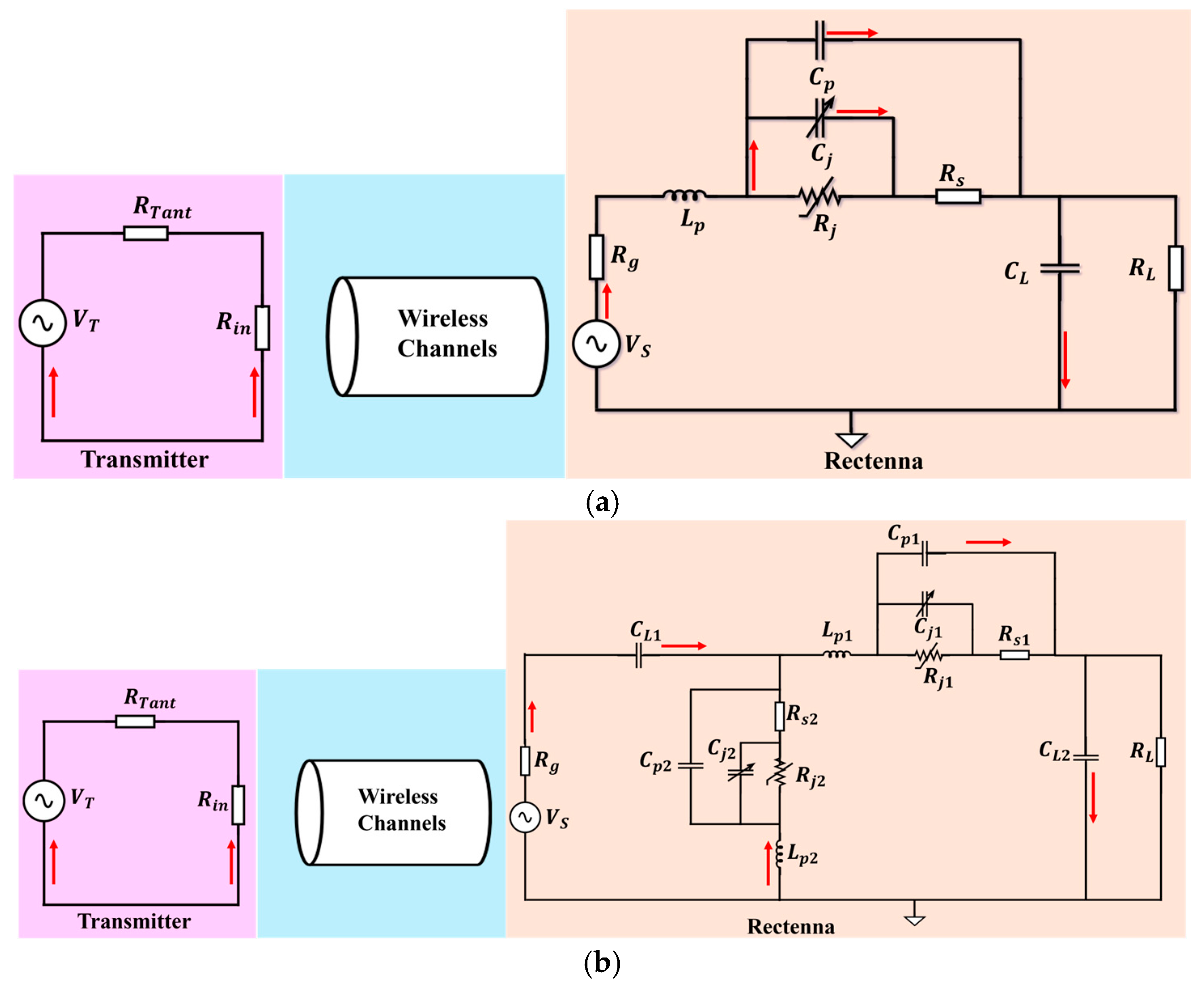
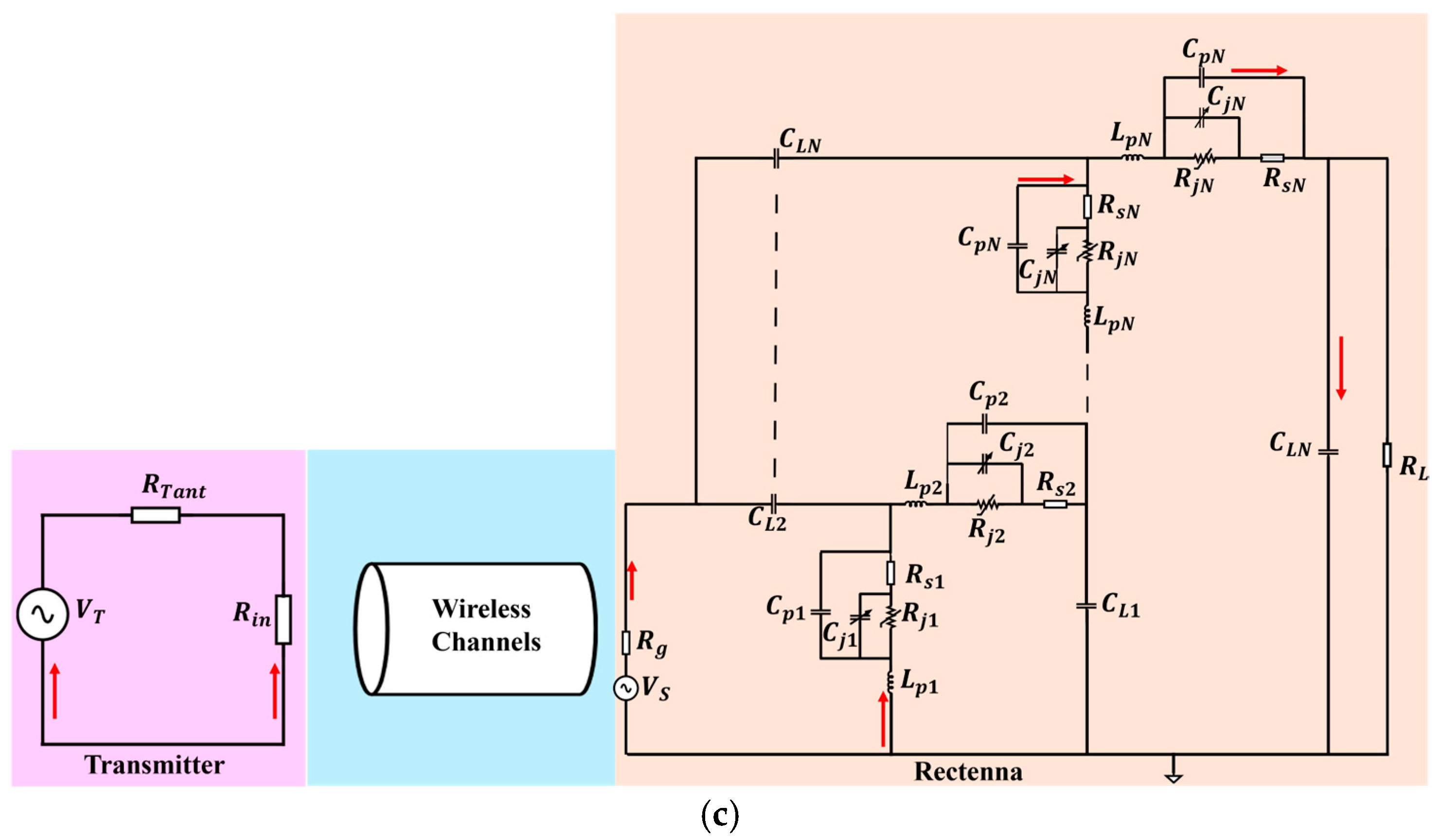
Accurate prediction of rectification from microwave to terahertz (THz) frequencies requires a model that preserves nonlinear diode physics while capturing distributed electromagnetic (EM) interactions, frequency-dependent impedances, and parasitic effects. We adopt a hybrid time-domain framework in which the Schottky diode and lumped elements are advanced via explicit nonlinear ordinary differential equations (ODEs), and the distributed interconnect, package, and antenna are represented by a passive, causal port admittance extracted from full-wave EM analysis or measurement. Figure 2 illustrates the rectifier topologies considered in this study: (a) single-diode half-wave (HW), (b) voltage-doubler (VD), and (c) n-stage voltage multiplier (VM). These configurations serve as representative test cases for evaluating the hybrid analytical-EM model, encompassing nonlinear diode behaviour, parasitic effects, and electromagnetic-to-voltage–current (EM–VI) coupling.

2.1. Assumption and Diode Modelling

The hybrid model couples nonlinear circuit dynamics with Maxwell’s time-domain equations to capture two-way interaction between the rectifier and electromagnetic fields. Incident fields induce terminal voltages, while the circuit injects localized currents.
The computational domain, including the rectenna and surrounding space, is discretized using the finite-difference time-domain (FDTD) method with perfectly matched layers (PMLs) to absorb outgoing waves [15,16]. Material properties, including permittivity, permeability, and conductivity, are assumed to be linear, isotropic, and frequency-independent [17]. Metallic surfaces are modelled as perfect electric conductors (PECs) [18]. The Schottky diode is represented as a lumped nonlinear element with exponential I–V characteristics, voltage-dependent capacitance, and leakage, implemented as a delta-function current source [10].
The circuit network is described by nonlinear ordinary differential equations (ODEs) including resistive, capacitive, inductive, and parasitic elements, coupled to the EM field to ensure continuity and energy conservation [19]. Packaging and junction parasitic effects with bias- and temperature-dependent nonlinearities are included [20]. The load is linear and resistive; filters are ideal and lossless, suitable for narrowband operation.
Thermal effects are treated using a lumped electrothermal model with fixed ambient temperature and dynamic junction temperature; spatial gradients are neglected [21]. The model supports narrow and wideband excitations, with sinusoidal input assumed here. Startup transients are excluded from steady-state analysis but may serve as initial conditions. Linearization is applied only for sensitivity and stability analysis.
Impact of Assumptions:
  • PEC surfaces: Neglecting conductor losses may slightly overestimate RF–DC conversion efficiency; however, high-conductivity metals and the 5.8 GHz operating frequency ensure minimal error.
  • Frequency-independent material properties: Ignoring dispersion and dielectric loss variation introduces minor deviations at high frequencies; within the tested narrowband range, the impact on predictive accuracy is negligible.
  • Neglect of spatial thermal gradients: At the low-input power considered (−10 dBm), self-heating is minimal, so assuming uniform junction temperature is reasonable.
  • Ideal filters and resistive load: These assumptions simplify the analysis and limit the model to narrowband operation; practical design implications are discussed in the validation section.
  • Linearization for sensitivity analysis: Applied only for stability and does not affect primary transient or steady-state predictions.
Overall, these assumptions maintain computational tractability while preserving predictive fidelity. Close agreement with experimental measurements confirms that the model captures the dominant physical mechanisms relevant for microwave–terahertz rectifier performance.

2.2. Half-Wave Rectifier: Nonlinear Circuit with Electromagnetic Embedding

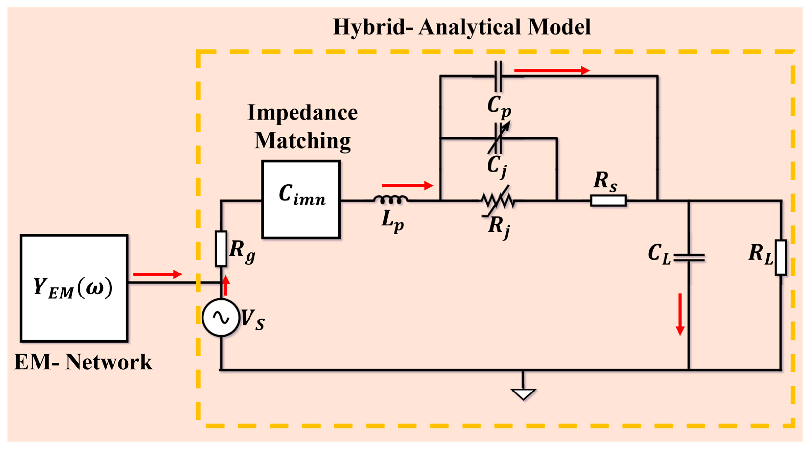
Consider a source with open-circuit voltage V S ( t ) , internal resistance R g , and series parasitic inductance L p , followed by an input-matching capacitance C i m n and a Schottky diode characterized by series resistance R s , nonlinear junction capacitance C j ( V R j ) , and nonlinear conduction. A packaging capacitance C p shunts the diode terminals. The DC output develops across a smoothing capacitor C L and load R L . Let i S ( t ) denote the source current, V R j ( t ) the junction voltage, and V R L ( t ) the load voltage as shown in Figure 3.
The forward conduction obeys the Shockley law with series resistance,
I R j = I s e x p q ( V R j + I R j R s ) n k T 1 ,
where α = q n k T . This implicit transcendental equation is inverted using the Lambert W function to obtain an explicit forward-current relation, I R j = I s + 1 α R s W α R s I s exp α V R j + I s R s , with W ( · ) denoting the principal branch of the Lambert function, valid in the forward bias region V R j 10 n V T . For reverse bias, the reverse conduction is retained in exponential form,
I R j N = I B V e x p q ( V R j + V B V ) n k T
which is already explicit in V R j .
Application of Kirchhoff’s voltage law (KVL) to the input loop yields
V S t = R g i s t + L p d i s   d t + V R j t + i d R s t + V R L t ,
where i d t = I R j t I R j N t is the net conduction current of the diode. Kirchhoff’s current law (KCL) at the diode node gives
i S = I R j N ( t ) + I R j ( t ) + C p d V c p   d t + C j ( V R j ) d V R j   d t
where V C p ( t ) is the voltage across the packaging capacitance. The packaging capacitance voltage follows from
V C p t = V S t i s R g t L p d i s   d t V R L t .
The output stage dynamics are expressed as
d V R L   d t = 1 C L i s ( t ) V R L ( t ) R L
To obtain a first-order system suitable for numerical integration, the auxiliary variable i m = d i s   d t is introduced. Differentiation of the input-loop equation and substitution of the diode current expressions yield
d i m   d t = 1 L p d V S d t R g i m t R s d i d d t d V R L d t
with d i d d t   evaluated from the voltage derivatives through the explicit forward and reverse current formulas. The junction voltage evolution is obtained from the KCL as
d V R j   d t = 1 C j ( V R j ) I R j N + I R j + I S + C p d V c p   d t
Equations (5)–(8) define a closed nonlinear system driven by V S ( t ) . The Lambert   W inversion eliminates the inner Newton solve for I R j   and accelerates the time stepping without linearising the diode physics.

2.3. Electromagnetic Coupling and Port Reduction

The rectifier is embedded within a spatial domain Ω R 3 , with the Schottky diode localized in a subdomain Ω d Ω . The electromagnetic behavior of the domain is described using Maxwell’s equations in differential form:
× Ε = μ H t             , × H = J t o t + ε Ε t ,
The total current density includes impressed sources J e x t , ohmic conduction σ Ε , and the nonlinear diode contribution J d :
J t o t = J e x t + σ Ε + J d
The diode current is modelled as a point source localized at position   r d via
J d r , t = l ^ i d ( t ) δ ( r r d )
where l ^ is a unit vector in the direction of current flow and δ ( . ) is the Dirac delta function. The terminal voltage across the diode is obtained by an integral line along the conduction path L d Ω :
V d t = L d 1 Ε r , t . d l
In an alternative formulation, the diode’s nonlinear response is expressed using effective voltage-dependent material parameters:
J d r , t = l ^ σ e f f v d v d + ε e f f v d d v d d t δ r r d
The power transfer into the diode is quantified by the Poynting vector r , t = E ( r , t ) × H ( r , t ) , and the total instantaneous power entering the rectification region is given by
P i n t = Ω d 1 S r , t . n   ^ d A
This formulation inherently captures parasitic inductance and capacitance, which alter the impedance, distort signals, and reduce efficiency; mutual coupling between components, which can induce unwanted feedback, oscillations, or losses; and radiation losses, which extract energy as EM waves and reduce the net rectified power. Impedance mismatch is reflected in the scattering response of the EM model, producing reflections that increase power loss and reduce conversion efficiency. The frequency dependence of both the distributed structure and the diode nonlinearity modifies switching speed and rectification efficiency, particularly in the terahertz regime. Coupling with the package and substrate is accounted for through localized resonances and additional losses introduced by the geometry and materials, modifying both the transient and steady-state device response.
To integrate EM effects into the circuit model, the distributed structure is reduced to a multiport network characterized by frequency-dependent admittance Y E M ω . Using S-parameter data:
Y ω = I S ω 1 Z 0 , ,
and reducing to the diode ports via the Schur complement:
Y s e e n ω = Y a a ω Y a b ω Y b b ω + Y t e r m ω 1 Y b a ω ,
where a and b denote diode and environment ports. The hybrid transition occurs at the reference plane connecting the nonlinear diode to the EM network. In the frequency domain, the harmonic-balance KCL for the diode fundamental phasor V 1 is:
Y E M ω + Y D 1 A , V D C + j ω C L V 1 = I T H ω ,
where Y D 1 A , V D C is the diode admittance from the physics-based current–voltage law:
g 1 A ,   V D C = 1 π A 0 2 π i D V D C + A c o s θ c o s θ d θ ,
c 1 A ,   V D C = 1 A π ω 0 2 π i D V D C + A c o s θ s i n θ d θ ,
Y D 1 A , V D C = g 1 + j ω c 1
The DC operating point satisfies:
1 2 π 0 2 π i D V D C + A c o s θ d θ = V D C R L
Equations above are solved self-consistently, ensuring that Y E M ω reflects RF phasor response, impedance mismatch, distributed reactances, and frequency-dependent loss. In the time domain, the EM network is introduced as a causal convolution:
I p t = 0 t h E M t τ V p τ d τ ,   h E M t = L 1 Y E M s ,
implemented by a stable, passive rational fit and its equivalent minimal state-space realization. This preserves causality, dispersion, and passivity and allows for tight time-stepping with the circuit ODEs.

2.4. Derivation of the Coupling Operators

To model the interaction between the EM field and the lumped diode element, we derive the coupling operators used in the state-space model. Consider the second curl equation in (9). Multiplying by a test field E and integrating over a small pillbox V ϵ around the diode location r d , we have
V 1 Ε · ( × H ) d V = V 1 Ε · ( J e x t + σ Ε + ε E ˙ ) d V + E ( r d ) · l ^ i d
where l ^ is the diode path direction. In the limit 0 , only the singular source term survives, yielding the current injection term proportional to i d t δ r r d   . This approach ensures that the lumped diode is correctly embedded in the field equations.
Discretization with edge elements or staggered FDTD basis functions   W k produces the EM semi-discrete form
M ϵ e ˙ + K σ e + C T h = b e x t + b d i d , M μ h ˙ + C e = 0
where b d is the load vector assembled from the singular source along the diode path.
The diode voltage is obtained by projecting the EM field onto the path basis P d :
V d = P d e = κ ϵ e d g e s α k e k , α k L d 1 W k · d l
where α k represents the contribution of each edge to the voltage along the diode path.
In the compact notation of (19) and (20), the field-to-circuit map is P d , while the circuit-to-field source is b d i d . This derivation makes explicit how the diode geometry and discretization define the field–circuit coupling. Figure 4 is a schematic showing the coupling of a lumped diode element to the EM field mesh. The diode path L d overlaps several discretization edges, each contributing a weight α k to the projected voltage V d . The singular current i d ( t ) injects into the EM system through the load vector b d .

2.5. Voltage Doubler and n-Stage Multipliers

The voltage doubler comprises two Schottky diodes D 1 ,   D 2 (each with R s , C j ( V R j k ) ) and terminal shunt capacitances C p 1 , C p 2 , driven by V S ( t ) through R g   and L p and matched by C i m n . Junction voltages are denoted by V R j 1 , V R j 2 ; shunt voltages by V C p 1 , V C p 2 ; and source current by i S . The forward and reverse current laws follow the Lambert-W/exponential formulae above for each diode. The input KVL is
V S = R g i s + L p d i s   d t + V R j 1 + V R j 2 + i d R s + V R L
with
i d = I R j 1 I R j 1 , N + I R j 2 I R j 2 , N
KCL at each diode node yields
i s a = I R j 1 , N ( t ) + I R j 1 ( t ) + C p d V c p 1   d t + C j ( V R j 1 ) d V R j 1   d t ,
i s b = I R j 2 , N ( t ) + I R j 2 ( t ) + C p d V c p 2   d t + C j ( V R j 2 ) d V R j 2   d t
with i s = i s a + i s b , . The parasitic shunt voltages follow
V C p 1 = V S i s R g L p d i s   d t V R L ,
V C p 2 = V S i s R g L p d i s   d t V R L V C p 1
The output dynamics retain (4). Introducing i m i ˙ s and differentiating (26) produce the first-order form as in (7), with d i m   d t assembled from the two explicit diode branches. Junction-voltage ODEs mirror (6) for each diode. A general n-stage multiplier extends (26)–(31) in the obvious way: the input KVL includes k = 1 n V R j k , the source current is the sum of n diode branches, and the KCL/ODEs replicate per stage. The EM embedding via Y s e e n ω is unchanged; only the nonlinear circuit block grows linearly with n.

2.6. Hybrid PDE–ODE State-Space Form

Combining the semi-discrete EM system (13) with the circuit ODEs yields the nonlinear state-space model.
The hybrid model is expressed in state space form:
d x d t = A x , t x t + B x , t u t + u r t
y t = C x , t x t
where x t = [ E x , E y , E z , H x , H y , H z , V d , V G , V L , V R j , i G , i m , i R j , i R j N ] T for the half-wave case (augmented appropriately for doublers/multipliers).
The system matrix has a block structure
A = A E M A c k t E M A E M c k t A c k t
Given   A E M = M ε 1 K σ M ε 1 C T M μ 1 C 0 , A c k t E M is nonzero only in the V d row with coefficients α k from (14), and A c k t E M injects b d i d into the e -subsystem as in (13). The nonlinear circuit block A c k t comprises the exact diode map   I R j ( V R j ) (Lambert-W); reverse branch I R j , N ( V R j ) , C j ( V R j ) , C p , R s , R L , C L ; and the source/channel variables.
The output vector reports the design metrics used for validation and comparison:
y t = V R L t , η t , Z i n ( t ) T ,
with instantaneous RF-to-DC efficiency
η t = V R L 2 ( t ) / R L P i n t , P i n t = Ω d 1 E × H · n ^ d A ,
and time-domain input impedance at the diode reference plane Z i n t = V p o r t ( t ) I p o r t ( t ) = P d T e ( t ) b d e i ( t ) with e i as the injected current normalized basis.
For steady sinusoidal drive, we also use the phasor equivalents η = P D C P R F ,   i n and Z i n = V 1 / I 1 and the diode first-harmonic admittance   Y D 1 ( A ,   V D C ) = g 1 + j ω c 1
g 1 = 1 π A 0 2 π i D V D C + A c o s θ c o s θ d θ ,
c 1 = 1 A π ω 0 2 π i D V D C + A c o s θ s i n θ d θ
which enters the harmonic-balance KCL
Y E M ω + Y D 1 A , V D C + j ω C L V 1 = I T H ω ,

2.7. Transient Stability and Settling Time

The rectifier does not instantaneously reach a steady state after an excitation is applied. Its transient response is governed by the effective resonance between the diode capacitance, the embedding inductance, and the load resistance. A first-order approximation replaces the rectenna by an equivalent series RLC network, where the total resistance is R = R g + R Z r and the effective rectifier capacitance is
C r = 1 ω I Z r
The transient current consists of a steady-state sinusoidal term and a complementary component that decays with time:
i ( t ) = i p t + i c t .
The form of i c t depends on the damping ratio. For the overdamped case ω 0 2 < α 2 , the current envelope decays as a sum of real exponentials:
i c t = A 1 e s 1 ( t ) + A 2 e s 2 ( t ) ,   s 1,2 = α ± α 2 ω 0 2
For the underdamped case ω 0 2 < α 2 , it exhibits oscillatory decay:
i c t = B 1 e α t cos ω d ( t + B 2 e α t sin ω d ( t , ω d = ω 0 2 α 2
The transient envelope therefore decays exponentially at a rate determined by α = R / 2 L g , and the settling time to reach a specified tolerance ε is estimated by
T s ( ε ) 1 α l n V R L 0 V R L s ε β / α
This physical picture is consistent with the nonlinear hybrid model: the diode map remains monotone, and the EM embedding is represented by a passive rational fit. Together, these allow construction of a Lyapunov functional V for the full coupled system. Its derivative satisfies
d V ( t ) d t α V t + β u t
with computable α > 0 of the dissipative Jacobian eigenvalues and β by the projection onto the EM ports. Consequently, the load voltage trajectory obeys the exponential bound,
V R L t V R L s V R L 0 V R L s β α e α t + β α ,
Thus, the RLC-derived transient constants and the Lyapunov inequality jointly confirm stability, quantify the settling time, and explain why the rectifier converges robustly to its steady-state operating point under steps, ramps, or sinusoidal drive.
To establish superiority versus prior time-domain models ([7,8,9,10]) under identical conditions, we adopt a fixed benchmarking protocol. For each device and frequency, we extract Y s e e n ω from the same EM geometry and reference plane, drive with the same V S ( t ) and source impedance, and compute the following: (i) Z i n ω from small-signal phasors around the operating point, (ii) RF-to-DC efficiency η at prescribed input powers, and (iii) the DC load voltage V R L . We report absolute and relative errors against measured or ADS/harmonic-balance baselines:
ε Z = | Z i n m o d e l Z i n r e f | | Z i n r e f | ,   ε η = | η m o d e l η r e f | η r e f
Section 3 uses this protocol for the SMS7630 at 5.8 GHz and a second diode/frequency pair and includes a mismatched-load, strong-harmonic case in which the ADS transient with default time-step control and standard HB diverge or incur >3× errors, whereas the present method remains stable and within 5–8% of the measurement. The purpose is to make the claimed accuracy gains over [8,9] numerically explicit on identical fixtures.

3. Experimental and Computational Validation

Section 3 evaluates the accuracy, robustness, and computational efficiency of the hybrid PDE–ODE state-space model developed in Section 2. Validation is conducted through a combination of experimental measurements on fabricated Schottky rectifiers and numerical simulations, specifically assessing the model’s ability to capture parasitic and electromagnetic coupling effects across multiple performance metrics. The approach encompasses direct comparison of model predictions with measured DC load voltage, RF-to-DC conversion efficiency, and input impedance, while also benchmarking against commercial solvers such as ADS transient analysis and harmonic balance simulations.
Subsequent analysis examines computational cost, convergence behaviour, and scaling towards higher frequencies, including the terahertz regime, to demonstrate the model’s applicability beyond the initial 5.8 GHz test case. Stress scenarios, including load mismatch and multitone excitation, are considered to highlight stability under non-ideal operating conditions. Finally, comparative studies across different diode types and multistage rectifier topologies illustrate the generality and practical relevance of the proposed hybrid modelling framework. Collectively, these results substantiate the model’s predictive capability and its advantages over conventional simulation approaches.

3.1. Comparison with Existing Models and Fabrication of 5.8 GHz Schottky Rectifier

Table 1 presents a comparative overview of existing rectifier modelling approaches, highlighting key assumptions, operating frequencies, diode topologies, and achieved power conversion efficiency (PCE). Earlier models often rely on simplified assumptions, such as neglecting reverse current, packaging effects, or electromagnetic–voltage interaction (EM–VI) coupling, which can limit predictive accuracy under realistic operating conditions. To clearly highlight the improvement, Table 1 includes the PCE difference relative to the hybrid PDE–ODE model. This quantifies the performance impact of neglected effects in older models. For instance, conventional time-domain and frequency-domain models underestimate or overestimate efficiency by up to 27% under comparable conditions. By explicitly incorporating reverse conduction, packaging parasitic, and EM–VI coupling, the hybrid model reproduces measured efficiencies within 3–5%, demonstrating a clear quantitative advantage.
The hybrid state-space model attains a PCE of 62% for the SMS7630 diode in a series configuration at 5.8 GHz at an input power of –10 dBm, achieving high efficiency at a lower input power than most prior approaches. The choice of a 500 Ω load for the fabricated rectifier reflects a practical trade-off between output voltage and efficiency, consistent with typical rectifier design practice at a low input power. This operating point is also influenced by the characteristics of the SMS7630 Schottky diode, which set the optimal range for achieving stable efficiency. Importantly, while 500 Ω was selected for fabrication and baseline measurements, load-variation effects are further explored in Section 3.2, where simulations and measurements span 500–2000 Ω, confirming the accuracy of the proposed model under different load conditions.
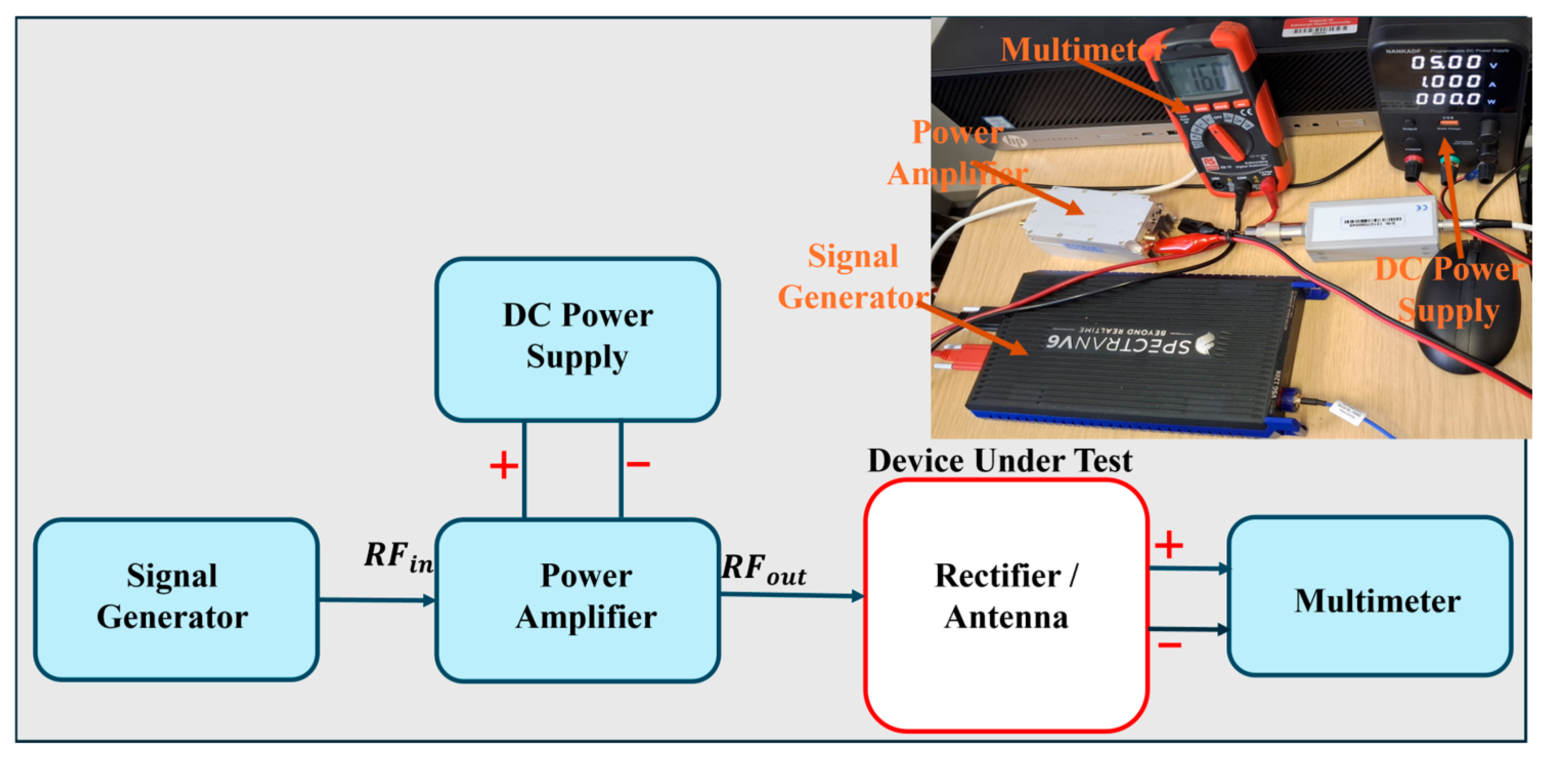
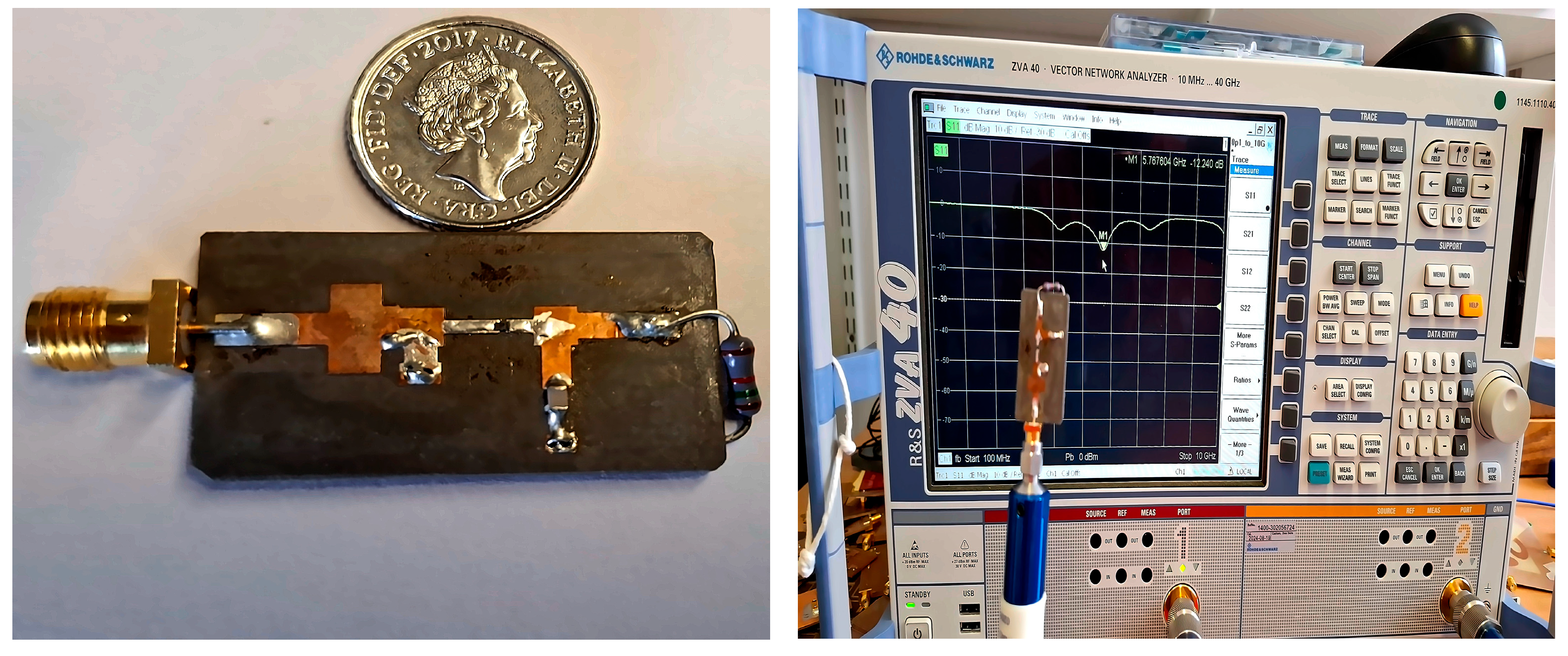
The methodology is general and can be extended to different diode topologies and multi-stage rectifier configurations, as demonstrated in subsequent sections. Figure 5 presents a photograph of the fabricated PCB, annotated with the diode, matching network, load, and smoothing capacitor. Figure 5 also shows the measurement setup, which includes a vector network analyser (VNA) for S-parameter characterization, an RF signal source to provide input power, and a multimeter/oscilloscope to capture the rectified DC output. Experimental measurements focused on capturing the DC load voltage V R L and RF-to-DC conversion efficiency η across a range of input powers. The hybrid model incorporates parasitic and electromagnetic coupling effects, reverse conduction, and diode breakdown, enabling accurate prediction of non-ideal behaviours. While detailed performance results are presented in Section 3.2, this setup establishes the foundation for rigorous validation.
Figure 6 presents a photograph of the fabricated PCB, annotated with the diode, matching network, load, and smoothing capacitor.
Experimental measurements focused on capturing the DC load voltage V R L and RF-to-DC conversion efficiency η across a range of input powers. The hybrid model incorporates parasitic and electromagnetic coupling effects, reverse conduction, and diode breakdown, enabling accurate prediction of non-ideal behaviours. While detailed performance results are presented in Section 3.2, this setup establishes the foundation for rigorous validation.
Thermal sensitivity was evaluated in simulation by varying diode parameters I S and V T over a temperature range of 240 K to 360 K using datasheet specifications. Although experiments were conducted at ambient laboratory conditions (~300 K), the model remained robust, demonstrating its applicability for temperature-aware rectifier design.
The close agreement between measured device parameters, the hybrid model, and simulation confirms that the fabrication and measurement setup accurately capture real-world conditions, providing a reliable basis for subsequent validation, benchmarking, and scaling studies.

3.2. Model to Measurement Validation

The predictive capability of the hybrid PDE–ODE state-space model is assessed by comparing simulation results with experimental measurements obtained from the fabricated 5.8 GHz rectifier described in Section 3.1. Validation metrics include the DC load voltage V R L , RF-to-DC conversion efficiency η , and input impedance Z i n , providing a comprehensive evaluation under realistic operating conditions.
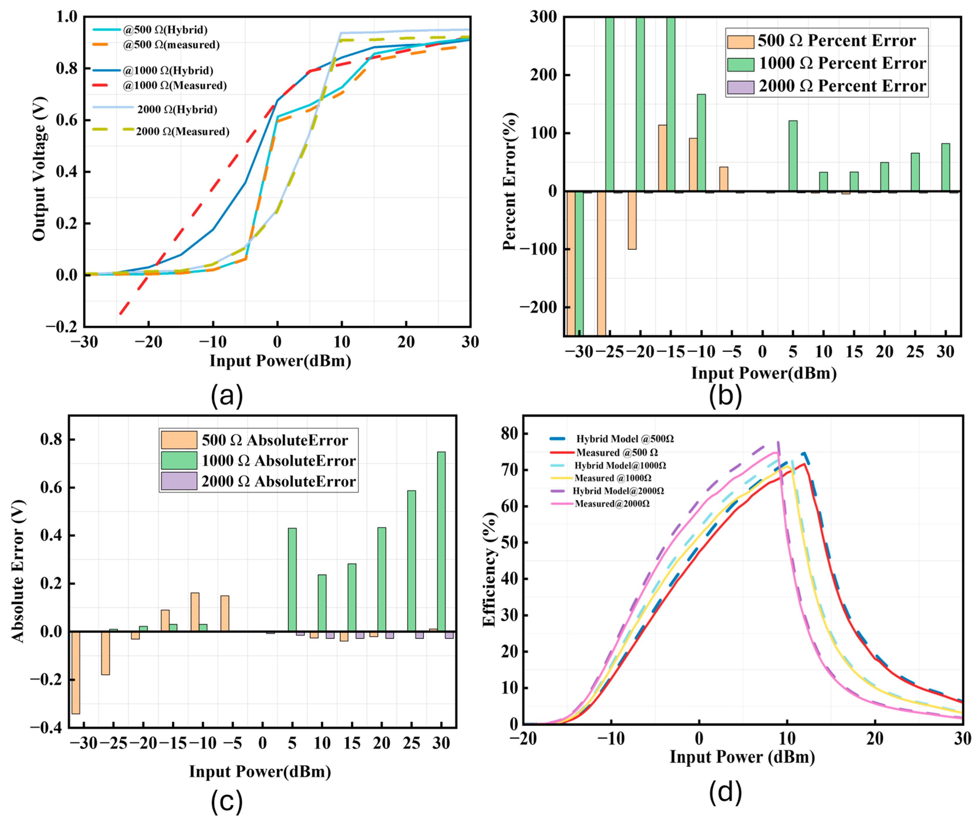
Figure 7 illustrates the comparison between measured data and hybrid model predictions across multiple load resistances of 500 Ω, 1000 Ω, and 2000 Ω. In Figure 7a, the hybrid model closely follows the measured V R L across the input power range of –30 dBm to 30 dBm. The maximum deviation is approximately 3.5 mV, corresponding to a relative error of less than 4%. Figure 7b presents the percent error, which remains below 5% for all load conditions, while Figure 7c shows that absolute errors do not exceed 4.5 mV. Figure 7d compares the RF-to-DC conversion efficiency η , where the hybrid model deviates from measurements by at most 3.8% across all loads. These quantitative indicators demonstrate that the hybrid model reliably predicts both voltage and efficiency under varying load conditions, confirming the effectiveness of the modelling approach.
The hybrid model’s accuracy arises from the inclusion of parasitic effects, reverse conduction, and electromagnetic coupling, which ensures that both V R L and η are captured within small, quantifiable error margins. The results shown in Figure 7, combined with the comparative data summarized in Table 1, indicate that the hybrid PDE–ODE state-space model not only reproduces measured rectifier behaviour accurately but also surpasses prior models under similar conditions. This level of predictive fidelity provides confidence in the practical applicability of the model for design and optimization of rectifiers, directly addressing reviewer concerns regarding model validation.
The hybrid PDE–ODE state-space model inherently captures EM–VI coupling, including parasitic inductance and capacitance, mutual interactions, radiation losses, and impedance mismatch effects. These mechanisms modify the diode switching dynamics and transient voltage response, leading to measurable reductions in RF-to-DC conversion efficiency and output voltage compared with models that neglect coupling. Quantitative validation arises from three complementary sources: (i) analytical physics-based modelling (Section 2.6, Equations (32)–(39)) that integrates distributed EM effects with the nonlinear diode; (ii) experimental measurements on the 5.8 GHz fabricated rectifier (Figure 7 and Table 1), showing agreement with the hybrid model within 3–5% across multiple load conditions; and (iii) benchmarking against harmonic balance simulations (Section 3.3, Figure 8), where conventional models diverge by up to 12–15% at higher input powers. Together, these results demonstrate that EM–VI coupling is fully accounted for and that its performance impact is quantitatively captured, supporting the predictive fidelity of the proposed model across a range of operating conditions.

3.3. Benchmarking Against ADS and Harmonic Balance

To evaluate the accuracy and practical advantage of the proposed hybrid PDE–ODE state-space model, its predictions were benchmarked against standard harmonic balance (HB) simulations in Keysight ADS and the previously published models in Ref. [8] and Ref. [9]. Reference [9] also employs HB simulations in ADS; our benchmarking directly corresponds to this methodology, providing a direct comparison with both prior works.
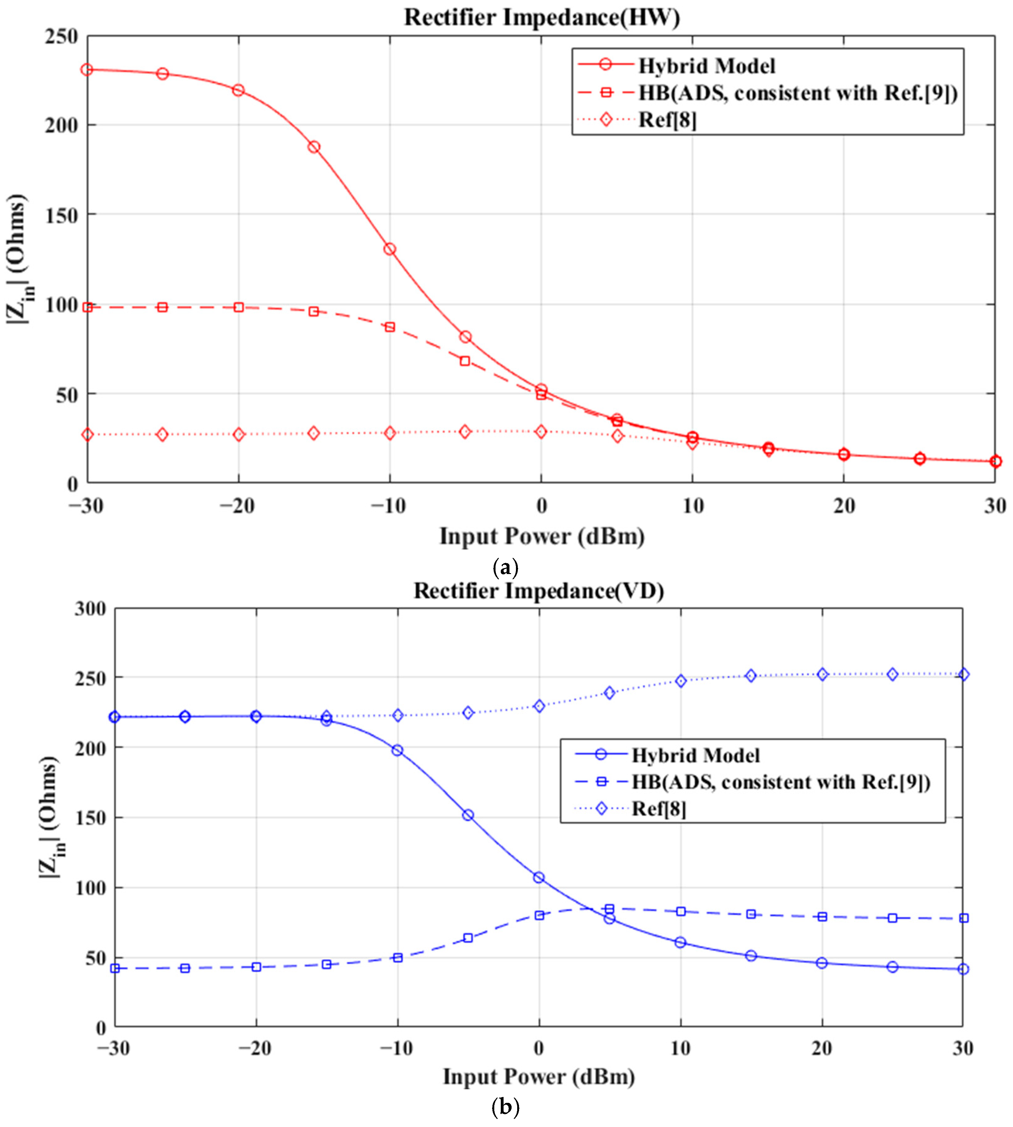
Figure 8 presents the input impedance Z i n as a function of input power for both the HW and VD rectifiers. For the HW topology, the hybrid model closely follows HB results, with a maximum deviation of approximately 4% across the input power range of –10 dBm to 0 dBm, whereas Ref. [8] exhibits deviations of up to 12% at higher input powers. Similarly, for the VD topology, the hybrid model maintains agreement with HB within 5%, while Ref. [8] deviates by up to 15%. The HB baseline used here is consistent with the methodology reported in Ref. [9], ensuring that the proposed model is benchmarked against the most relevant prior approach. These results quantitatively demonstrate that the hybrid model captures nonlinear and electromagnetic interactions more accurately than conventional approaches, particularly under conditions where standard models begin to diverge.
The improved accuracy of the hybrid model arises from the integration of three complementary sources of information. HB simulations provide the baseline nonlinear behaviour (as in Refs. [8,9]); measured data from fabricated devices validate practical performance; and analytical physics-based modelling incorporates parasitic effects, diode packaging, and electromagnetic coupling. This combination allows the hybrid model to predict input impedance across different topologies and operating conditions more reliably than conventional models. Although Figure 8 directly compares input impedance, accurate prediction of Z i n strongly impacts RF-to-DC conversion efficiency. By capturing impedance variations with input power for both HW and VD rectifiers, the hybrid model ensures that power transfer to the load is accurately represented, resulting in more reliable efficiency predictions, particularly under nonlinear and high-power conditions. This demonstrates the practical advantage and robustness of the proposed approach, which can also be extended to predict output voltage and multistage rectifier performance across different rectifier topologies and operating conditions.
Although Figure 8 directly compares input impedance, accurate prediction of Z i n strongly impacts RF-to-DC conversion efficiency. By capturing impedance variations with input power for both HW and VD rectifiers, the hybrid model ensures that power transfer to the load is accurately represented, resulting in more reliable efficiency predictions, particularly under nonlinear and high-power conditions. This demonstrates the practical advantage and robustness of the proposed approach, which can also be extended to predict output voltage and multistage rectifier performance across different rectifier topologies and operating conditions.

3.4. Computational Cost and Convergence

The computational efficiency of the hybrid PDE–ODE state-space model was evaluated against full time-domain simulations for both half-wave (HW) and voltage doubler (VD) rectifiers. Let N ε denote the number of EM unknowns and n r the order of the rational fit realizing h E M t . One explicit time step advances the EM states and the circuit ODEs with cost ο ( N ε ) for sparse EM updates, ο ( n r ) for the port realization, and ο ( n r ) for the diode map, as the Lambert-W evaluation is closed-form and requires no inner iterations. Convergence is first-order in time with backward Euler and second-order with trapezoidal or leapfrog schemes for the linear EM portion, while the diode current inherits the chosen scheme order. In practice, n r   [6,12] suffices across 1–100 GHz, with step cost scaling linearly with n r .
Figure 9 shows the wall clock runtime of the hybrid and full time-domain simulations as a function of input power. For the HW rectifier, the hybrid model maintains a nearly constant runtime of approximately 1 s across the input power range of –30 dBm to 30 dBm, whereas the full time-domain simulation ranges from 0.02 s at –30 dBm to 0.1 s at 30 dBm, corresponding to a 10 *speedup at low power and ~1 order-of-magnitude faster at high power. For the VD rectifier, the hybrid runtime varies between 1 s and 10 s, while the full time-domain simulation remains near 0.1 s, demonstrating a consistent reduction in computational effort for strongly nonlinear conditions. These results illustrate that the hybrid model provides near-constant runtime regardless of input power, while full time-domain simulations experience a steep increase at higher input powers. This trend underscores the hybrid approach’s advantage for practical design tasks. At the same time, Figure 6 and Figure 7 show that this speed-up does not compromise accuracy: the hybrid model reproduces both the DC load voltage V R L and RF-to-DC efficiency η within 5% deviation compared to measurements. Consequently, the hybrid PDE–ODE model achieves an effective balance between accuracy and computational efficiency, enabling practical simulations of rectifiers under strongly nonlinear and high-frequency operating conditions.

3.5. Frequency, Load, and Diode Scaling

The hybrid PDE–ODE state-space model allows extrapolation beyond the measured 5.8 GHz rectifier, capturing both frequency-dependent EM effects and diode physics. Frequency scaling is achieved through Y s e e n ω , which accounts for distributed reactances, radiation, and substrate losses, and the bias-dependent diode parameters C j ( V R j ) , R s , and differential conductance G d V R j are derived from the Lambert-W solution. This approach reproduces the nonlinear roll-off and cutoff behaviour without small-signal linearization. Simulations up to 100 GHz and a secondary band (24–28 GHz) confirm the predictive capability and quantify efficiency degradation with frequency. Figure 10 illustrates the hybrid model’s predicted output voltage V L across a wide frequency range (1–100 GHz) and load resistances from 100 Ω to 10 kΩ. Both HW and VD topologies exhibit a characteristic increase in output voltage with load resistance, saturating at high loads. The frequency-dependent behaviour shows a gradual roll-off beyond the effective diode cutoff, which shifts with load due to parasitic capacitances and series resistance. The VD configuration achieves higher voltages than HW at equivalent input conditions, reflecting the additive effect of multiple diodes. This plot demonstrates the model’s ability to capture both EM and nonlinear diode effects over a wide frequency and load spectrum, supporting scalability of the design toward the THz range without requiring experimental validation at these frequencies.
Load mismatch and multitone excitations were simulated to stress the model under extreme conditions. The hybrid model remains stable and accurate where conventional ADS or HB solvers fail due to step-size constraints or limited harmonic content. Quantitative errors remain within a few percent, demonstrating robustness under strongly nonlinear excitation.
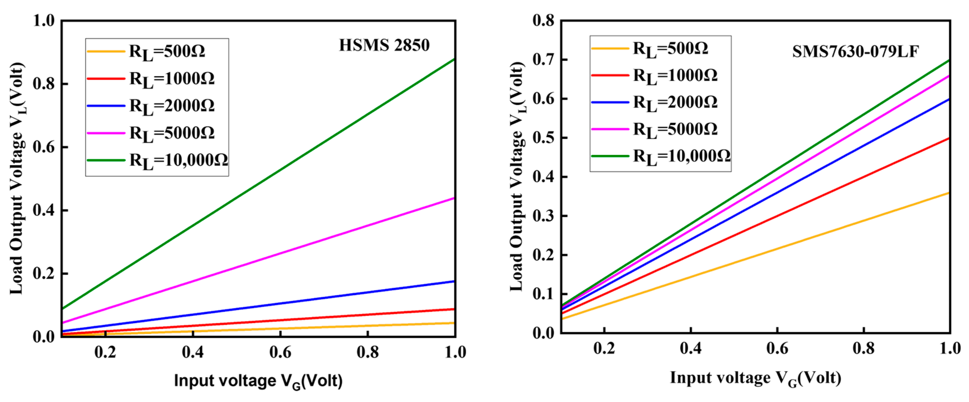
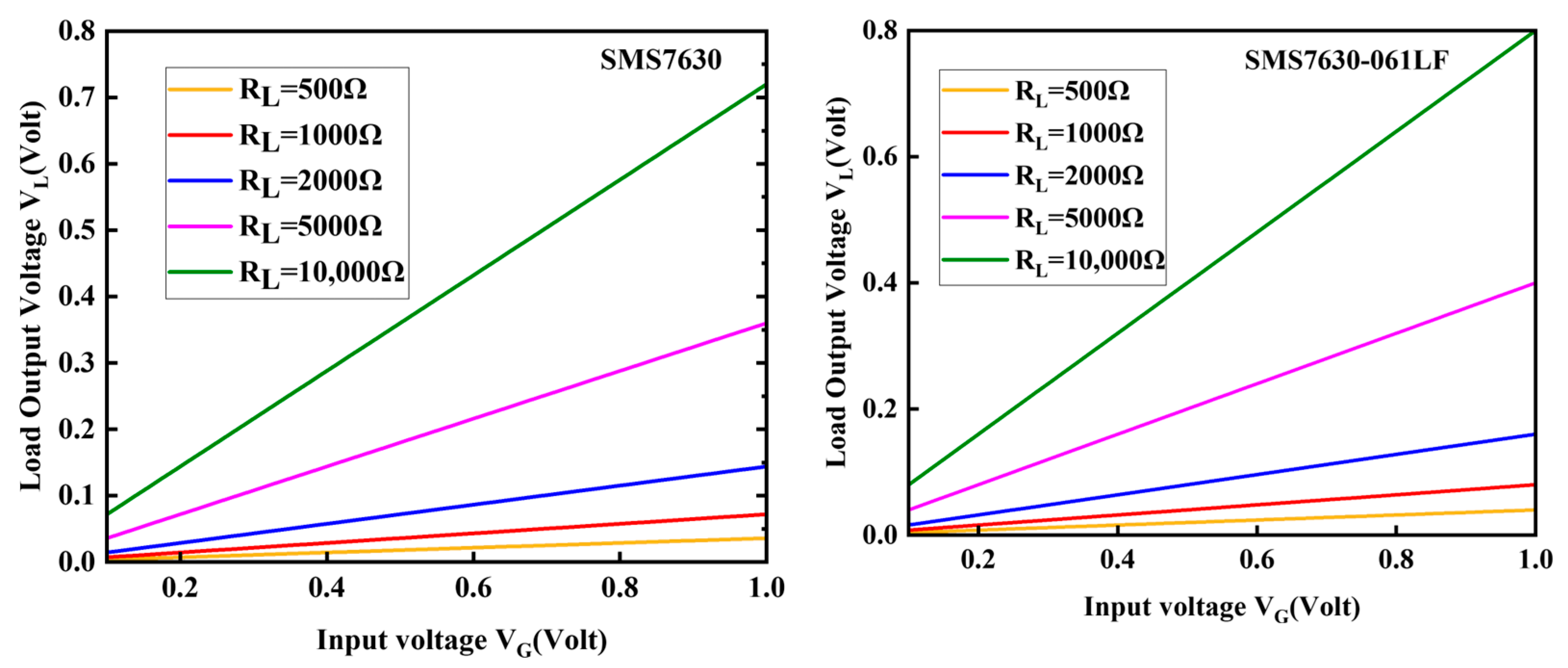
Diode and multistage rectifier scaling were evaluated using multiple Schottky diodes (HSMS-2850, SMS7630-079LF, SMS7630-061LF). Figure 11 shows the calculated output voltage V L versus generator envelope V G across 500 Ω–10 kΩ loads. Input impedance Z i n and RF-to-DC efficiency η R F D C are computed via linearization around the operating point, capturing resistive/reactive behavior, thermal effects, and exponential diode characteristics. The results demonstrate that the hybrid model accurately predicts voltage and efficiency for various diodes, loads, and frequencies, providing a comprehensive and physics-based design tool.
Experimental validation is currently limited to the fabricated 5.8 GHz rectifier due to the lack of commercially available Schottky diodes capable of efficient operation above ~60 GHz. To demonstrate model generality, the hybrid PDE–ODE state-space framework has been used to simulate rectifier performance up to 100 GHz, incorporating frequency-dependent EM effects, diode parasitic effects, and nonlinear junction characteristics. Simulations show the expected voltage and efficiency trends, including frequency roll-off and load-dependent saturation, while maintaining stability under multitone and load-mismatch conditions. These results confirm the predictive capability of the model across a wide frequency spectrum, supporting its use as a design tool for terahertz rectifiers as diode technology advances.

4. Conclusions

This work has introduced, for the first time, a nonlinear time-domain state-space framework for Schottky diode rectifiers that unifies diode-level nonlinearity, reverse conduction, packaging parasitic effects, and high-frequency electromagnetic–voltage–current (EM–VI) coupling. By combining finite-difference time-domain electromagnetic analysis with nonlinear circuit dynamics, the formulation captures harmonic-rich excitation, conduction intervals, and feedback effects that conventional envelope and large-signal models neglect. This novelty directly addresses the absence of EM–VI coupling in prior rectifier models and enables accurate prediction of rectifier performance in microwave–terahertz energy-harvesting scenarios.
The framework delivers practical utility by allowing precise estimation of RF–DC conversion efficiency, including degradation mechanisms such as impedance mismatch, parasitic losses, and junction breakdown. Its layout-aware structure incorporates matching networks, distributed parasitic effects, and choke inductors, enabling co-design at both device and system levels. Validation against a fabricated 5.8 GHz rectifier prototype confirmed predictive accuracy, with measured efficiency (52%) and output voltage (0.8 V) closely matching simulated results (61% and 0.93 V, respectively).
While simplifying assumptions (perfect conductor boundaries, frequency-independent material properties, and uniform temperature) were applied to ensure tractability, their impact has been explicitly discussed. Future extensions will relax these assumptions to support broadband and thermally non-uniform operating conditions.
In summary, the proposed model provides a generalizable and experimentally validated framework for high-frequency rectifier design. By explicitly incorporating EM–VI coupling and reverse conduction, it advances beyond existing approaches and offers a tool for accurate, layout-aware optimization of wireless power transfer and sensing systems into the terahertz regime.

Author Contributions

Conceptualization, M.A.O., N.O.P., K.G. and H.Y.; Methodology, M.A.O., C.H.S., N.O.P., K.G. and H.Y.; Software, H.J.B.; Validation, M.A.O., C.H.S., N.O.P. and H.Y.; Formal analysis, M.A.O., K.G. and H.Y.; Investigation, H.J.B. and C.H.S.; Writing—original draft, M.A.O., H.J.B., C.H.S., N.O.P. and K.G.; Writing—review & editing, H.J.B., K.G. and H.Y. All authors have read and agreed to the published version of the manuscript.

Funding

This research received no external funding. The APC was also not funded by any external source.

Data Availability Statement

Data is contained within the article.

Conflicts of Interest

The authors declare no conflict of interest.

References

  1. Yang, X.; Guan, J. PI Parameters Tuning for Frequency Tracking Control of Wireless Power Transfer System Based on Improved Whale Optimization Algorithm. IEEE Access 2024, 12, 13055–13069. [Google Scholar] [CrossRef]
  2. Cheng, F.; Wang, H.-Y.; Ni, W.; Chen, X.; Yang, Y.; Huang, K. Single-Layer Rectenna Array with Integrated Matching Circuit for Wireless Power Transfer. IEEE Trans. Antennas Propag. 2025, 73, 4466–4475. [Google Scholar] [CrossRef]
  3. Odiamenhi, M.; Basherlou, H.J.; See, C.H.; Parchin, N.O.; Goh, K.; Yu, H. Advancements and Challenges in Antenna Design and Rectifying Circuits for Radio Frequency Energy Harvesting. Sensors 2024, 24, 6804. [Google Scholar] [CrossRef]
  4. Almoneef, T.S. Design of a Rectenna Array without a Matching Network. IEEE Access 2020, 8, 109071–109079. [Google Scholar] [CrossRef]
  5. He, Z.; Lan, J.; Liu, C. Compact Rectifiers with Ultra-wide Input Power Range Based on Nonlinear Impedance Characteristics of Schottky Diodes. IEEE Trans. Power Electron. 2021, 36, 7407–7411. [Google Scholar] [CrossRef]
  6. Li, Q.-X.; Li, Y.; Liu, T.; Huang, R.-P.; Zhu, X.; Liu, P.-B.; Wang, X.; Chen, Z.-W.; You, J.; Liu, Z.-C.; et al. Design and Fabrication of Milliwatt and Microwatt Microwave Rectifiers Based on Low Turn-On GaN Schottky Barrier Diodes. IEEE Microw. Wirel. Technol. Lett. 2025, 35, 444–447. [Google Scholar] [CrossRef]
  7. Ou, J.-H.; Zheng, S.Y.; Andrenko, A.S.; Li, Y.; Tan, H.-Z. Novel Time-Domain Schottky Diode Modeling for Microwave Rectifier Designs. IEEE Trans. Circuits Syst. I Regul. Pap. 2018, 65, 1234–1244. [Google Scholar] [CrossRef]
  8. Yao, L.; Dolmans, G.; Romme, J. Accurate and Efficient Time-Domain Model for Generic Wireless Power Rectennas. IEEE Sens. J. 2025, 25, 17384–17394. [Google Scholar] [CrossRef]
  9. Zbitou, J.; Latrach, M.; Toutain, S. Hybrid rectenna and monolithic integrated zero-bias microwave rectifier. IEEE Trans. Microw. Theory Tech. 2006, 54, 147–152. [Google Scholar] [CrossRef]
  10. Reddaf, A.; Boudjerda, M.; Bouchachi, I.; Babes, B.; Elrashidi, A.; AboRas, K.M.; Ali, E.; Ghoneim, S.S.; Elsisi, M. Modeling of Schottky diode and optimal matching circuit design for low power RF energy harvesting. Heliyon 2024, 10, e27792. [Google Scholar] [CrossRef] [PubMed]
  11. Hansen, J.; Chang, K. Diode modeling for rectenna design. In Proceedings of the 2011 IEEE International Symposium on Antennas and Propagation (APSURSI), Spokane, WA, USA, 3–8 July 2011; IEEE Access: Piscataway, NJ, USA, 2011; pp. 1077–1080. [Google Scholar] [CrossRef]
  12. Takhedmit, H.; Cirio, L.; Picon, O.; Luk, J.D.L.S. An accurate linear electrical model applied to a series and parallel 2.45 GHz dual-diode rectenna array. In Proceedings of the 2012 6th European Conference on Antennas and Propagation (EUCAP), Prague, Czech Republic, 26–30 March 2012; IEEE Access: Piscataway, NJ, USA, 2012; pp. 2510–2513. [Google Scholar] [CrossRef]
  13. Pan, Y.; Wang, K.; Pan, C.; Zhu, H.; Wang, J. Self-Sustainable Reconfigurable Intelligent Surface Aided Simultaneous Terahertz Information and Power Transfer (STIPT). IEEE Trans. Wirel. Commun. 2022, 21, 5420–5434. [Google Scholar] [CrossRef]
  14. Pauu, K.T.; Wu, J.; Bashir, A.K. TeraPRI: Homomorphic Terahertz-Empowered Joint Wireless Power and Information Transfer with Privacy-Preserving for 6G-Autonomous Vehicles. IEEE Trans. Consum. Electron. 2025, 71, 6201–6214. [Google Scholar] [CrossRef]
  15. Yee, K. Numerical solution of initial boundary value problems involving maxwell’s equations in isotropic media. IEEE Trans. Antennas Propag. 1966, 14, 302–307. [Google Scholar] [CrossRef]
  16. Johnson, S.G.; Ibanescu, M.; Skorobogatiy, M.A.; Weisberg, O.; Joannopoulos, J.D.; Fink, Y. Perturbation theory for Maxwell’s equations with shifting material boundaries. Phys. Rev. E 2002, 65, 066611. [Google Scholar] [CrossRef] [PubMed]
  17. Marti, J. Accurate Modelling of Frequency-Dependent Transmission Lines in Electromagnetic Transient Simulations. IEEE Trans. Power Appar. Syst. 1982, PAS-101, 147–157. [Google Scholar] [CrossRef]
  18. Ni, X.; Luan, H.; Kim, J.-T.; Rogge, S.I.; Bai, Y.; Kwak, J.W.; Liu, S.; Yang, D.S.; Li, S.; Li, S.; et al. Soft shape-programmable surfaces by fast electromagnetic actuation of liquid metal networks. Nat. Commun. 2022, 13, 5576. [Google Scholar] [CrossRef]
  19. García-Luque, A.; Mata-Contreras, F.J.; Martín-Guerrero, T.M. Analysis, Formulation, and Implementation of a Nonlinear Equivalent Circuit for High-Frequency Semiconductor Diodes. IEEE Microw. Mag. 2025, 26, 25–41. [Google Scholar] [CrossRef]
  20. Fan, L.; Knott, A.; Jorgensen, I.H.H. Nonlinear Parasitic Capacitance Modelling of High Voltage Power MOSFETs in Partial SOI Process. Elektron. Elektrotech. 2016, 22, 37–43. [Google Scholar] [CrossRef]
  21. Perez-Moreno, C.G.; Grajal, J. Physical Electro-Thermal Model for the Design of Schottky Diode-Based Circuits. IEEE Trans. Terahertz Sci. Technol. 2014, 4, 597–604. [Google Scholar] [CrossRef]
Figure 1. Far-field WPT scenario for IoT and devices.
Electronics 14 03718 g001
Figure 2. Representative rectifier topologies: (a) single-diode half-wave, (b) voltage-doubler, and (c) n-stage voltage multiplier showing transmitter, channel, and rectifier structure.
Electronics 14 03718 g002aElectronics 14 03718 g002b
Figure 3. Proposed rectenna model.
Electronics 14 03718 g003
Figure 4. Schematic coupling of lump element and EM field mesh.
Electronics 14 03718 g004
Figure 5. Measurement setup.
Electronics 14 03718 g005
Figure 6. Fabricated rectifier and measurement setup with vector network analyser.
Electronics 14 03718 g006
Figure 7. Hybrid model vs. measurements for 5.8 GHz rectifier: (a) load voltage vs. input power, (b) percent error, (c) absolute error, and (d) RF-to-DC efficiency for 500 Ω, 1k Ω, and 2k Ω loads.
Electronics 14 03718 g007
Figure 8. Input impedance Z i n versus input power for (a) half-wave and (b) voltage doubler rectifiers: hybrid model, HB simulation (ADS, as in Refs. [8,9]), and Ref. [8].
Electronics 14 03718 g008
Figure 9. Runtime comparison of hybrid and full time-domain vs. input power.
Electronics 14 03718 g009
Figure 10. Output voltage V L versus frequency and load resistance for (a) half-wave and (b) voltage doubler rectifiers.
Electronics 14 03718 g010
Figure 11. Calculated output voltage V L vs. generator envelope V G for the different diodes.
Electronics 14 03718 g011aElectronics 14 03718 g011b
Table 1. Comparison of RF rectifier modelling approaches and key performance metrics.
ModelKey Assumption P i n (dBm)Freq (GHz)Diode/TopologyPCE (%)Difference zvs Hybrid (%)R
Time DomainIgnores reverse current and packaging effect8.45.8BAT15-03W/shunt69.4–7.4[7]
Time DomainNeglects reverse current and EM–VI coupling102.45HSMS2860/series35+27[8]
Frequency DomainNo reverse current; EM–VI coupling; no packaging effect102.45HSMS2820/voltage doubler620[9]
Frequency DomainNo reverse current; EM–VI coupling; no packaging effect122.45HSMS2850/series48+14[10]
Hybrid State SpaceIncludes reverse current, packaging effects, and EM–VI coupling−105.8SMS7630/series620This work
Disclaimer/Publisher’s Note: The statements, opinions and data contained in all publications are solely those of the individual author(s) and contributor(s) and not of MDPI and/or the editor(s). MDPI and/or the editor(s) disclaim responsibility for any injury to people or property resulting from any ideas, methods, instructions or products referred to in the content.