Article

Efficiency Analysis of Bridgeless Three-Level PFC Circuits Based on Modal Segment Integration Method

College of Electrical Engineering and New Energy, China Three Gorges University, Yichang 443002, China
*
Authors to whom correspondence should be addressed.
Electronics 2025, 14(18), 3592; https://doi.org/10.3390/electronics14183592
Submission received: 10 August 2025 / Revised: 7 September 2025 / Accepted: 9 September 2025 / Published: 10 September 2025

Abstract

Traditional methods for evaluating power electronic converter efficiency heavily rely on simulations and often lack theoretical support, which can lead to inaccuracies and limit effective design optimization. To address these shortcomings, this paper proposes a modal segment integration method based on a device loss model. The analysis begins with the operating principles of the proposed circuit topology. A detailed power loss model is then established and applied to representative operating modes. Using the modal segment integration method, the total loss over a full operating cycle is calculated. Theoretical analysis estimates the system efficiency exceeds 98%. To validate the proposed method, a 1 kW experimental prototype with a 400 V DC output is built. The results show that the maximum error between the theoretical and experimental efficiency is less than 0.4%. This method offers a reliable theoretical basis for efficiency evaluation of three-level converter topologies and supports the structural design and performance optimization of power electronic systems.

1. Introduction

With the constant development of power electronics technology, rectifier devices have been widely used in new energy vehicles, LED drives, and industrial automation. Among them, high-efficiency multilevel rectifiers have become the focus of research [1,2,3,4,5,6]. To meet international standards such as IEEE 519 [7] and IEC 61000−3−2 [8], rectifiers must have a high power factor, high current sinusoidality, and low total harmonic distortion (THD). Currently, power factor correction (PFC) is the most commonly used technical solution. Among them, the bridgeless three-level PFC rectifier demonstrates superior performance in reducing switching voltage stress and achieving high efficiency [9,10,11,12,13,14,15,16], and has received continuous attention from scholars worldwide.
Currently, high efficiency and high power density are key objectives in rectifier design, and they are crucial for system efficiency analysis and evaluation. Scholars worldwide have conducted extensive research on the efficiency improvement and loss optimization of three-level PFC rectifiers [17,18,19,20]. In [17], a bridgeless three-level PFC rectifier topology was proposed based on neutral-point capacitor voltage division. By reducing device voltage stress and optimizing current paths, the system efficiency was improved. In [18], a single-stage full-bridge boost PFC converter incorporating a passive snubber with a coupled inductor was proposed. The snubber effectively suppressed voltage spikes across the switches, reduced voltage stress and switching losses, and improved overall conversion efficiency. In [19], a single-stage current-fed boost PFC converter suitable for high-voltage applications was proposed. By forming a resonant tank with the transformer’s leakage inductance and the parasitic capacitance of the rectifier diodes, zero-current switching (ZCS) was achieved, which effectively reduced switching losses and improved the power factor. In [20], a current-controlled variable inductor was introduced into a single stage PFC boost rectifier to reduce system losses. Although the above literature has made positive progress in topology optimization, modulation strategies and loss control, the existing efficiency analysis methods mostly focus on simulation or experimental verification. These methods lack systematic, theoretical analysis, which means we cannot quickly assess the efficiency characteristics of the topology scheme at the design stage. Therefore, further improvement is needed.
In this paper, a modal segment integration method based on device loss model is proposed to analyze the system efficiency of the new bridgeless three-level PFC rectifier. Compared with traditional methods that rely on simulation or experiment, the proposed method is more systematic and has a stronger theoretical basis. It can quickly and accurately evaluate the efficiency of the topology during the design stage, helping to improve design efficiency. Firstly, the operating principle of the circuit topology is analyzed, including its operating modes, key waveform, and voltage stresses. Then, the power device loss model is established, which is combined with the typical operating modes. The modal segment integration method is used to calculate the average power loss of the whole cycle, and derive the system efficiency. Finally, an experimental prototype with an input voltage of 220 V/20 kHz, rated power of 1 kW, and DC output voltage of 400 V is built based on this proposed bridgeless three-level PFC circuit topology. This prototype is used to verify the proposed method and assess the accuracy and feasibility of its theoretical analysis.

2. Analysis of Topology and Its Working Process

2.1. Circuit Topology

This paper proposes a bridgeless three-level power factor correction (PFC) rectifier topology, as shown in Figure 1. The circuit includes the switches S1–S3, the diodes D1–D8, the DC-link capacitors C1 and C2, and input inductor L. During the positive half-cycle of the grid voltage, diodes D1 and D4 conduct, while diodes D2 and D3 conduct during the negative half-cycle. The switching tubes (S1–S3) are used to achieve three-level voltage conversion between the two bridge legs.

2.2. Analysis of Work Processes

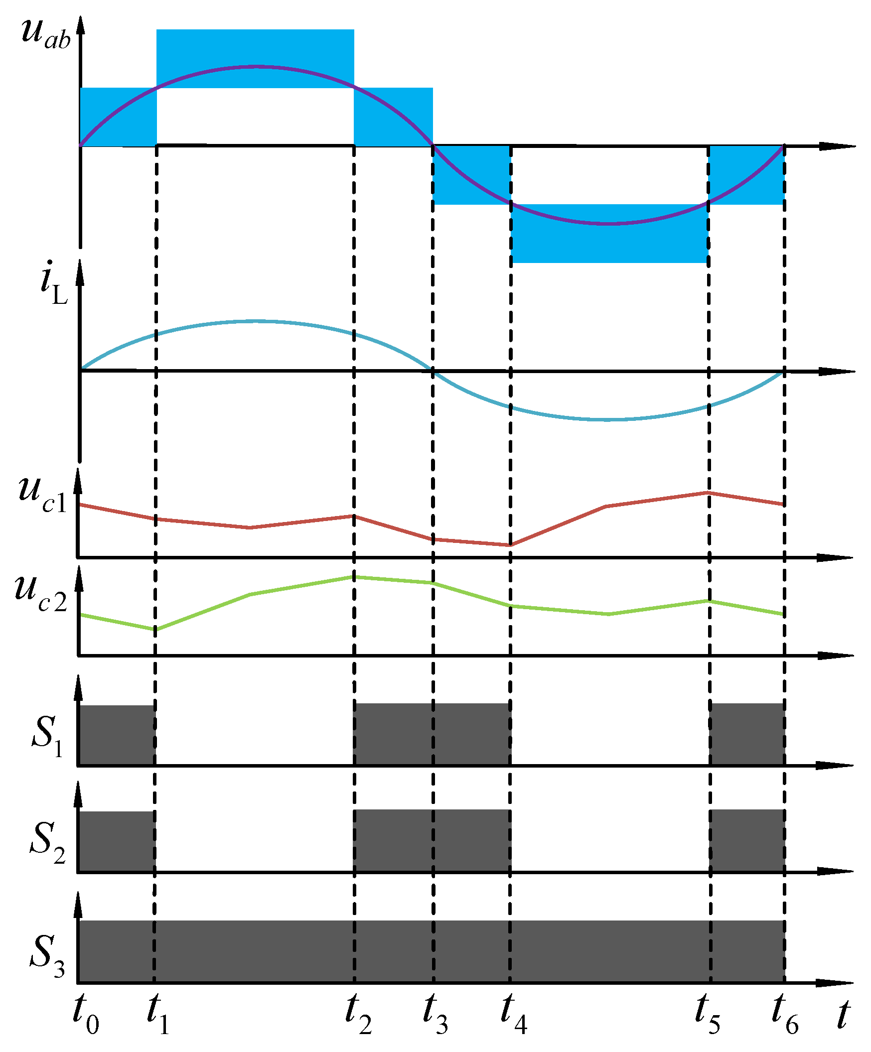
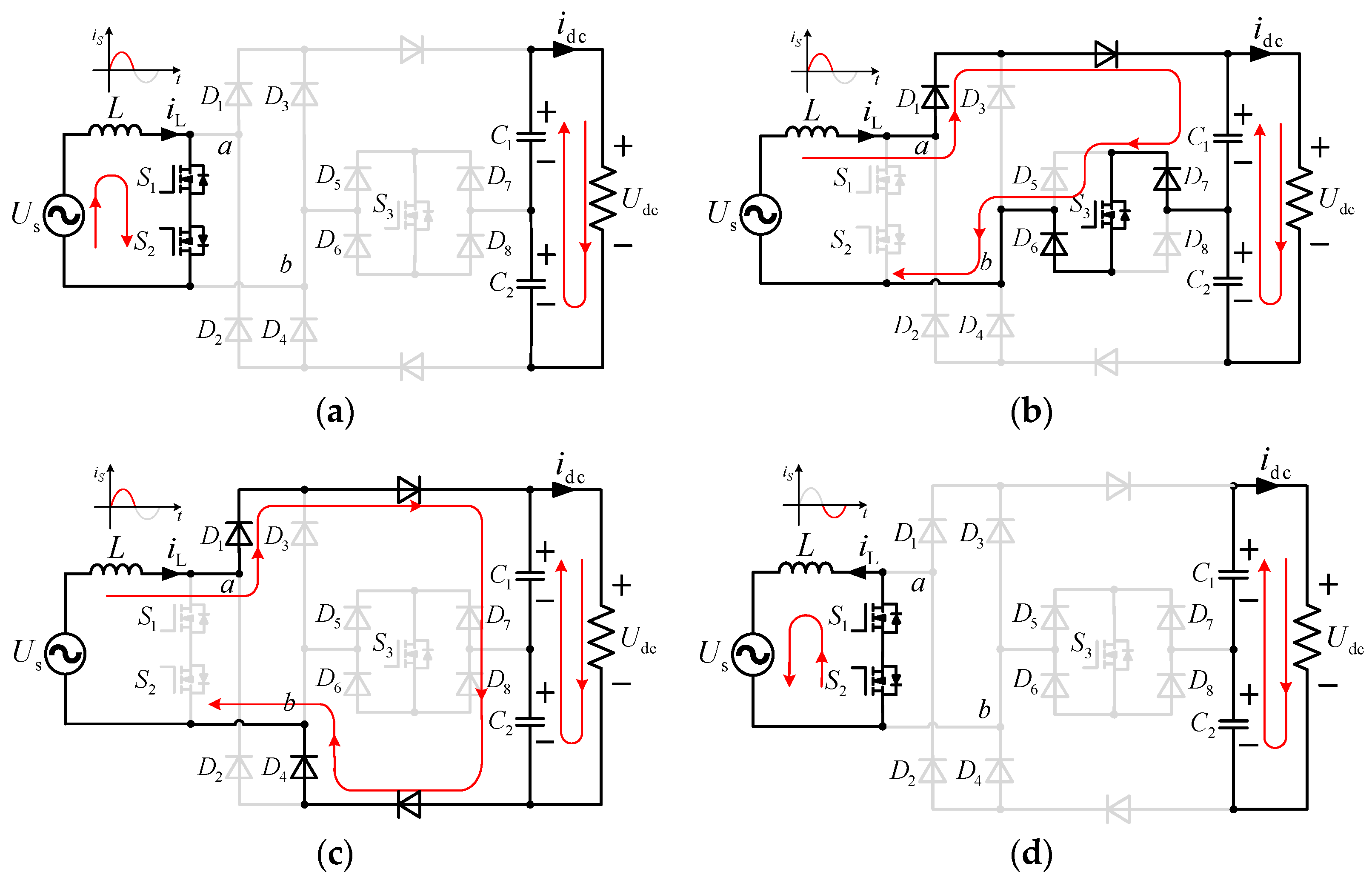
To verify the circuit’s effectiveness, the topology shown in Figure 1 is analyzed. As shown in Figure 2, the key waveforms over one power-line cycle are presented, and the circuit operates symmetrically during the positive and negative half cycles. To help readers understand, Figure 3 shows the current path diagrams of the six operating modes. Figure 3a–c show the three operating states of the circuit during the positive half-cycle and Figure 3d–f show the three operating states during the negative half-cycle.
Mode 1: As shown in Figure 3a, during the positive half-cycle of the grid voltage, S3 turns off, and S1 and S2 turn on. In this state, the power source charges the inductor L through S1 and S2. The inductor stores energy, and the current iL increases. Meanwhile, capacitors C1 and C2 discharge and supply power to the load RL. The bridge leg voltage Uab = 0.
Mode 2: As shown in Figure 3b, during the positive half-cycle of the grid voltage, S1 and S2 turn off and S3 turns on. In this state, inductor L discharges and charges capacitor C1. The current then flows through diode D1, capacitor C1, diode D7, switch S3, and diode D6. At this point, the bridge leg voltage Uab = Udc/2.
Mode 3: As shown in Figure 3c, the circuit operates during the positive half-cycle of the grid voltage and the switches S1, S2, and S3 are off. The power source delivers energy to capacitors C1, C2, and load RL through inductor L. The inductor current iL decreases. The bridge leg voltage Uab = Udc.
Mode 4: As shown in Figure 3d, during the negative half-cycle of the grid voltage, S3 turns off and S2 turns on. In this state, the power source charges the inductor L through S1 and S2. The inductor stores energy, and the current iL rises. In the meantime, capacitors C1 and C2 discharge and supply power to the load RL. The bridge leg voltage Uab = 0.
Mode 5: As shown in Figure 3e, the circuit works during the negative half-cycle of the grid voltage. S1 and S2 are off, while S3 is on. In this process, the inductor L releases energy and charges capacitor C2, and current flows through diode D5, switch S3, diode D8, capacitor C2, and diode D2. At this point, the bridge leg voltage Uab = Udc/2.
Mode 6: As shown in Figure 3f, the circuit operates during the negative half-cycle of the grid voltage and S1, S2, and S3 turn off. During this process, the power source supplies energy to capacitors C1 and C2, as well as to the load RL, through inductor L. The inductor current iL decreases during this time. At this time, the bridge leg voltage Uab = Udc.
The voltage stress characteristics of each MOSFET and diode in the proposed bridgeless three-level PFC circuit can be determined based on the above modal analysis. Table 1 shows the maximum voltage stress across each switching device.

3. Loss Analysis and Efficiency Estimation

This section analyzes the power devices losses in the bridgeless three-level circuit. Most of the losses are attributed to the diodes and MOSFETs. The loss calculation formulas are derived according to the method in [21].

3.1. Diode Loss Analysis

The three main loss components of the fast recovery diode include turn-on loss, conduction loss, and turn-off loss:
P D - O N = 1 2 f C I F ( V F R V F ) t fr
where P D - O N is the turn-on loss, f C is the switching frequency at 5 kHz, I F is the diode forward current, and V F R is the maximum diode forward recovery voltage. V F is the diode forward voltage drop, and t fr is the diode forward recovery time.
P D - C O N = V F I D ( A V ) + r D I D ( R M S ) 2
where P D - C O N is the conduction loss, I D ( A V ) is the average value of the diode current, I D ( R M S ) is the real-valued mean of the diode current, and r D is the diode conduction internal resistance.
P D - O F F = 1 4 f C I D ( R M ) K f V R t rr
where P D - O F F is the turn-off loss, I D ( R M ) is the maximum value of reverse recovery current, K f is the temperature coefficient, V R is the reverse voltage, and t rr is the reverse recovery time.
The total loss of the fast recovery diode is
P D = P D - O N + P D - C O N + P D - O F F

3.2. Loss Analysis of Power Switching Devices

The turn-on loss of the MOSFET device is mainly due to the energy discharged from its output capacitance C g . This loss is expressed as follows:
P Q - ON = 1 2 f C C g U o 2
where f c is the switching frequency, C g is the MOSFET’s equivalent output capacitance, and U 0 is the instantaneous turn-on voltage.
The equation used to calculate the conduction loss of the MOSFET device is
P Q - CON = I Q ( R M S ) 2 R Q
where P Q - CON is the conduction loss and I Q ( R M S ) is the root mean square value of the MOSFET current.
The turn-off loss is computed as follows:
P Q - OFF = 1 2 f c U o I L t fr
where P Q - OFF is the turn-off loss and t fr is the switch-on rise time.
Equations (3)–(14) give the MOSFET turn-on loss caused by the equivalent output capacitance. Since the output capacitance C g varies nonlinearly with the drain-source voltage, it is corrected to the datasheet value C o s s , leading to the form of Equation (8). On this basis, the reverse-recovery related loss of the diode, the conduction loss, and the turn-off loss are further included to form the total loss model of the MOSFET. The total loss of the MOSFET switches is as follows:
P Q = 2 3 f C C o s s U o 2 + 1 4 f c I D ( R M ) K f V R t r r + P Q C O N + P Q O F F
where P Q is the total loss of the MOSFET switches, f c is the switching frequency, C o s s is the specific output capacitance value taken from the MOSFET datasheet, I D ( R M ) is the maximum value of reverse recovery current, K f is the temperature coefficient, V R is the reverse voltage, and t rr is the reverse recovery time.
Equations (4)–(8) can be used to calculate the losses for a power-line cycle. However, the circuit topology parameters, such as the switching frequency f c , the average diode current I D ( A V ) , the rms diode current I D ( R M S ) , the rms switching tube current I Q ( R M S ) , and the turn-on instantaneous voltage U 0 , have not been determined. These parameters will be solved in the following section.
When switch S1 is turned on, the inductor voltage is v L = v g V dc , and when S1 is turned off, it becomes v L = v g V dc 2 . According to the principle of inductor volt-second balance, it can be derived that
D n ( v g V dc ) + ( 1 D n ) v g V dc 2 = 0
where D n is the ratio of the on-time of switch S1 within one switching period to the total switching period.
After simplification, it is derived as D n = 2 v g V dc 1 .
However, to make the inductor current track the AC input voltage and present a sinusoidal waveform, it is necessary to increase the duty cycle under stable load conditions. According to the inductor characteristics, the increased Δ i g can be expressed as follows:
D f ( v g V dc ) + ( 1 D f ) v g V dc 2 = L f Δ i g T s
After simplification, the result is
D f = 2 v g V dc 1 2 L f Δ i g V dc T s
If Δ D be expressed as 2 L f Δ i g V dc T s , then it is given by D f = D n + Δ D . Therefore, the final duty cycle of the controller consists of the steady-state duty cycle D n and the dynamic duty cycle Δ D . D n can be designed as a feed-forward voltage compensator, while Δ D tracks the reference AC input current i g * .
The expression for the instantaneous value of the duty cycle is given in differential form:
D t = ( 2 v g V d c 1 ) 2 L f V d c T s d i g / d t
To calculate the average duty cycle for each modal time period, integrate Equation (11). The average duty cycle D ¯ t from interval θ i ~ θ j can then be expressed as follows:
D ¯ t = 1 θ j θ i θ i θ j D t ( θ ) d θ
Substituting into Equation (4), the following can be obtained:
D ¯ t = 1 θ j θ i θ i θ j ( ( 2 v g V d c 1 ) 2 L f V d c T s d i g d t ) d θ
Furthermore, since
v g = v g m a x s i n θ
the average duty cycle can be further obtained:
D ¯ t = 1 θ j θ i 2 v g ,   max   V d c ( cos ( θ i ) cos ( θ j ) ) ( θ j θ i ) 2 L f V d c T s ( i g ( θ j ) i g ( θ i ) )
The RMS expression for the switching device’s current in the θ i ~ θ j interval is
I r m s = 1 θ j θ i θ i θ j i ( θ ) 2 d θ
In the interval θ i ~ θ j , the average current of the switching device is i ( θ ) a v g = k × i a v g , and the rms value of the switching device current is i ( θ ) r m s = k × i r m s , where k = 0, 1, or D ¯ t .

3.3. Estimation of Efficiency

In this paper, regarding the switching devices, the model STW26NM60N is selected for S1 and S2, and STP40NF20 is selected for S3, and the diode is STTH30RQ06. According to their datasheet, the main parameters are as follows: For STW26NM60N, t f r = 25 ns, t r r = 50 ns, and R Q = 0.135 Ω. For STP40NF20, t f r = 20 ns, t r r = 45 ns, and R Q = 0.045 Ω. For STTH30RQ06, V R R M = 600 V, I F A V M = 30 A, V F R = 16 V, V F = 1.6 V, t f r = 150 ns, t r r = 35 ns, r D = 7.1 mΩ, and I D ( R M ) = 18 A.
To accurately assess the total switching loss of the three-level PFC circuit over a power-line cycle, this paper uses a modal segment integration method to model and analyze the energy loss of the power devices based on the established device loss model. The cycle period [ 0 , 2 π ] is divided into six operating modes, namely [ 0 , θ 1 ] , [ θ 1 , θ 2 ] , [ θ 2 , π ] , [ π , θ 3 ] , [ θ 3 , θ 4 ] , and [ θ 4 , 2 π ] . Each mode corresponds to an angular range, [ θ m 1 , θ m ] , where m = 1, 2, 3, 4, 5, or 6. The operating states of the MOSFET and diode are explicit in each mode. The corresponding on-state currents, voltage stresses, and turn-on and turn-off behaviors can be determined for each mode, so the average power loss of the devices can be calculated independently.
The total loss of the MOSFET in the m-th interval is P Q k , m , and the cycle-averaged loss of the MOSFET is expressed as follows:
P Q total   = 1 2 π m = 1 6 k = { S 1 , S 2 , S 3 , S 4 } P Q k , m θ m θ m 1
The total loss of the diode in the m-th interval is P D j , m , and the cycle-averaged loss of the diode device is expressed as follows:
P D total   = 1 2 π m = 1 6 j = { D 1 , D 2 , D 3 , D 4 } P D j , m θ m θ m 1
The total switching losses are
P total   = 1 2 π m = 1 6 k P Q k , m + j P D j , m θ m θ m 1
In the modulation strategy of the three-level rectifier, the amplitude-normalized sine wave is chosen as v ref ( θ ) = m ^ sin ( θ ) . When m ^ = 1 , the intersection of the reference waveform and the intermediate zero-level carrier occurs at θ = arcsin ( ± 0.5 ) = ± π 6 . To further simplify the derivation of modal integrals for device losses, this paper sets the following: θ 0 = 0 , θ 1 = π / 6 , θ 2 = 5 π / 6 , θ 3 = π , θ 4 = 7 π / 6 , θ 5 = 11 π / 6 , and θ 6 = 2 π . The rectifier’s efficiency at different operating conditions is calculated and simulated by substituting specific device parameters into established power loss models. The devices selected for the calculations are the STW26NM60N model (for S1, S2,) and STTH30RQ06 model (for S3), and the STTH30RQ06 fast recovery diode (for D1–D8). The relevant device parameters, such as on-resistance, reverse recovery time, and output capacitance, are all from the device datasheet. The power-line cycle [ 0 , 2 π ] is divided, and the effective and average values are substituted into the aforementioned loss expression. With the switching frequency f s = 20   kHz , the loss value of each power device in different modal intervals can be obtained. According to this, the average loss power of the whole cycle can be obtained. The specific loss distribution, calculated from Equations (1)–(20), is shown in Figure 4.
As shown in Figure 4, the diode’s main loss is conduction loss, while the MOSFET’s main loss is turn-on loss. At rated power, the total loss is 19.36 W, and the efficiency is 98.03%.

4. Experimental Simulation and Verification

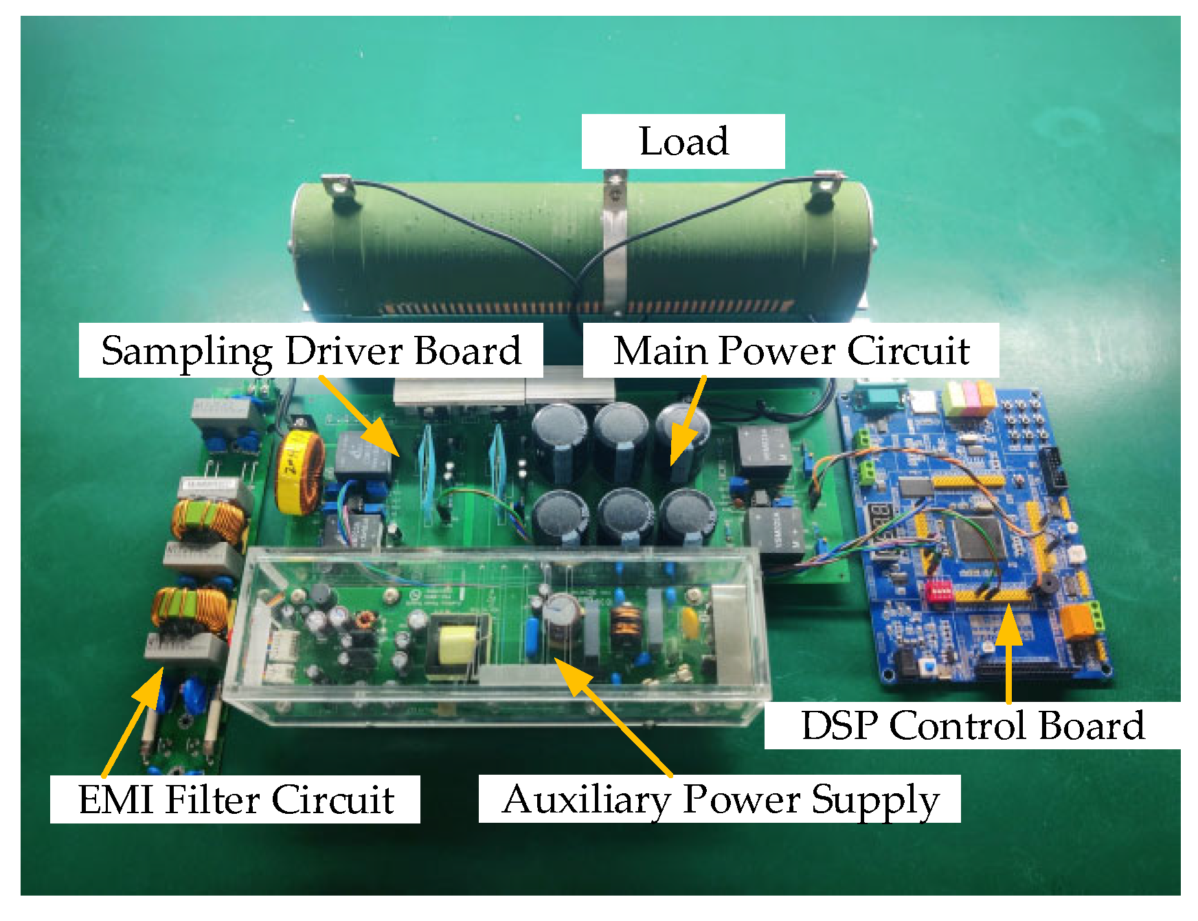
In order to verify the effectiveness of the proposed topology and modal segment integration method, a 1 kW bridgeless three-level PFC experimental prototype is constructed. Figure 5 shows the experimental prototype, and the related parameters are listed in Table 2. The input inductor is selected to ensure that the input current can follow the input voltage during power factor correction and achieve good dynamic response. Based on the system power level and control strategy, the inductance is chosen as 2.5 mH. Capacitors C1 and C2 are used as split DC-link capacitors to form the three-level voltage and keep the output voltage stable. According to the circuit requirements and experimental results, each capacitor is selected as 2000 μF.
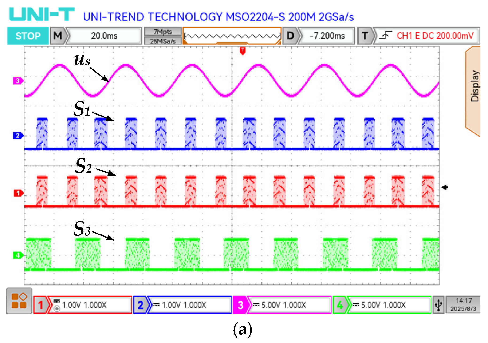
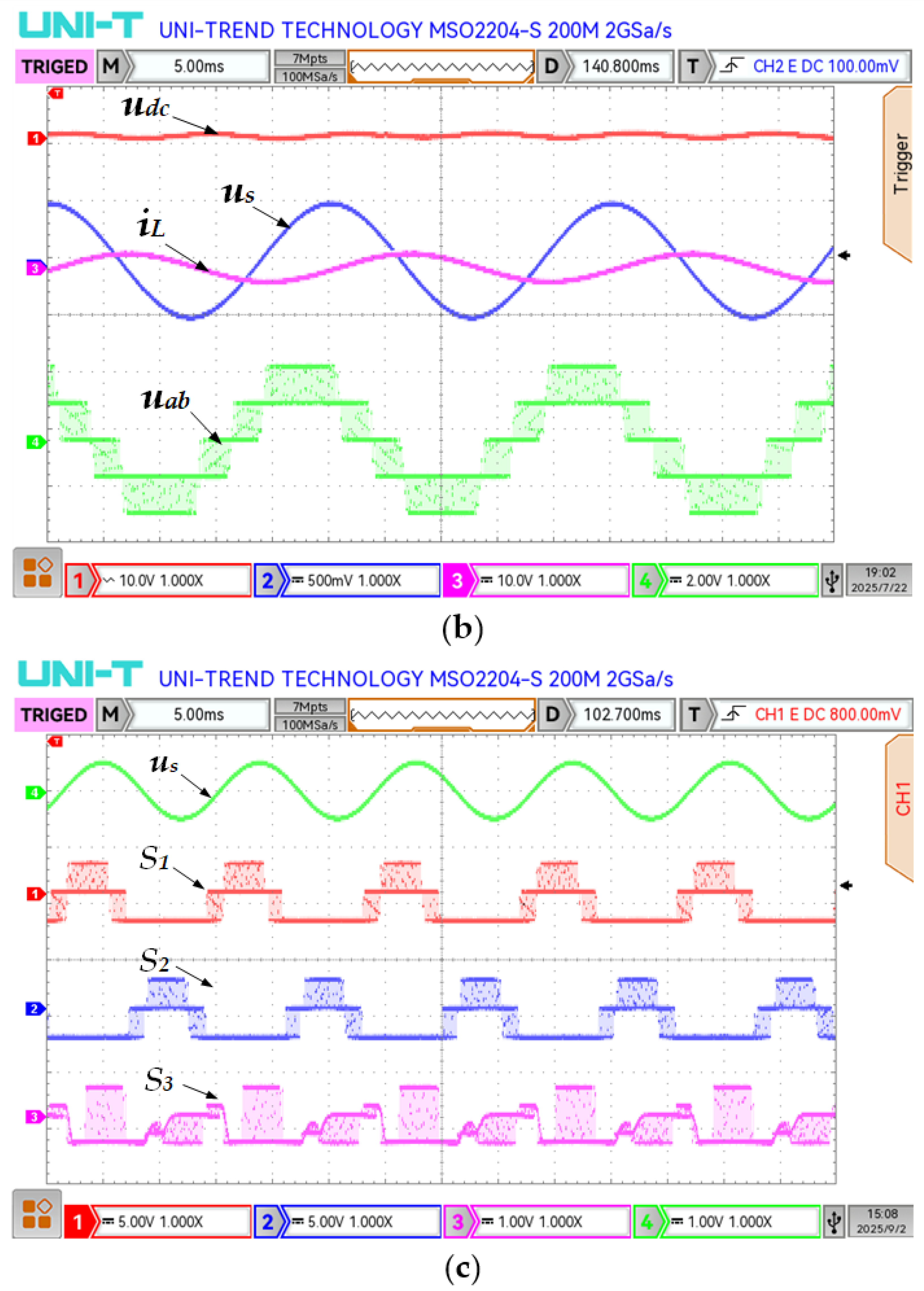
The steady-state experimental results of the proposed topology are shown in Figure 6. In this figure, udc and iL denote the voltage and current on the grid side, respectively. udc represents the output voltage on the DC side, while uab stands for the bridge-arm voltage. Additionally, uc1 and uc2 indicate the voltages across capacitors C1 and C2, respectively.
Figure 6a shows the switching pulse distribution waveforms for switches S1, S2, and S3. From the figure, within a single operating cycle, the operational duration of S1 and S2 constitutes a relatively small proportion.
Figure 6b, the input voltage uab has three-level voltages as follows: 0, ±udc/2, and ±udc. The proposed topology is confirmed to be a three-level circuit. And the waveform of input voltage udc is in phase with the waveform of input current iL, meeting the unity power factor. The output DC voltage udc is stable at 400 V.
Figure 6c shows the voltage waveforms of switches S1, S2, and S3. The voltages of S1 and S2 range from 0 to 400 V, while S3 varies between 0 and 200 V. The waveform of S3 appears irregular due to dead time and diode conduction during current commutation, which cause small dips and distortions at the switching transitions.
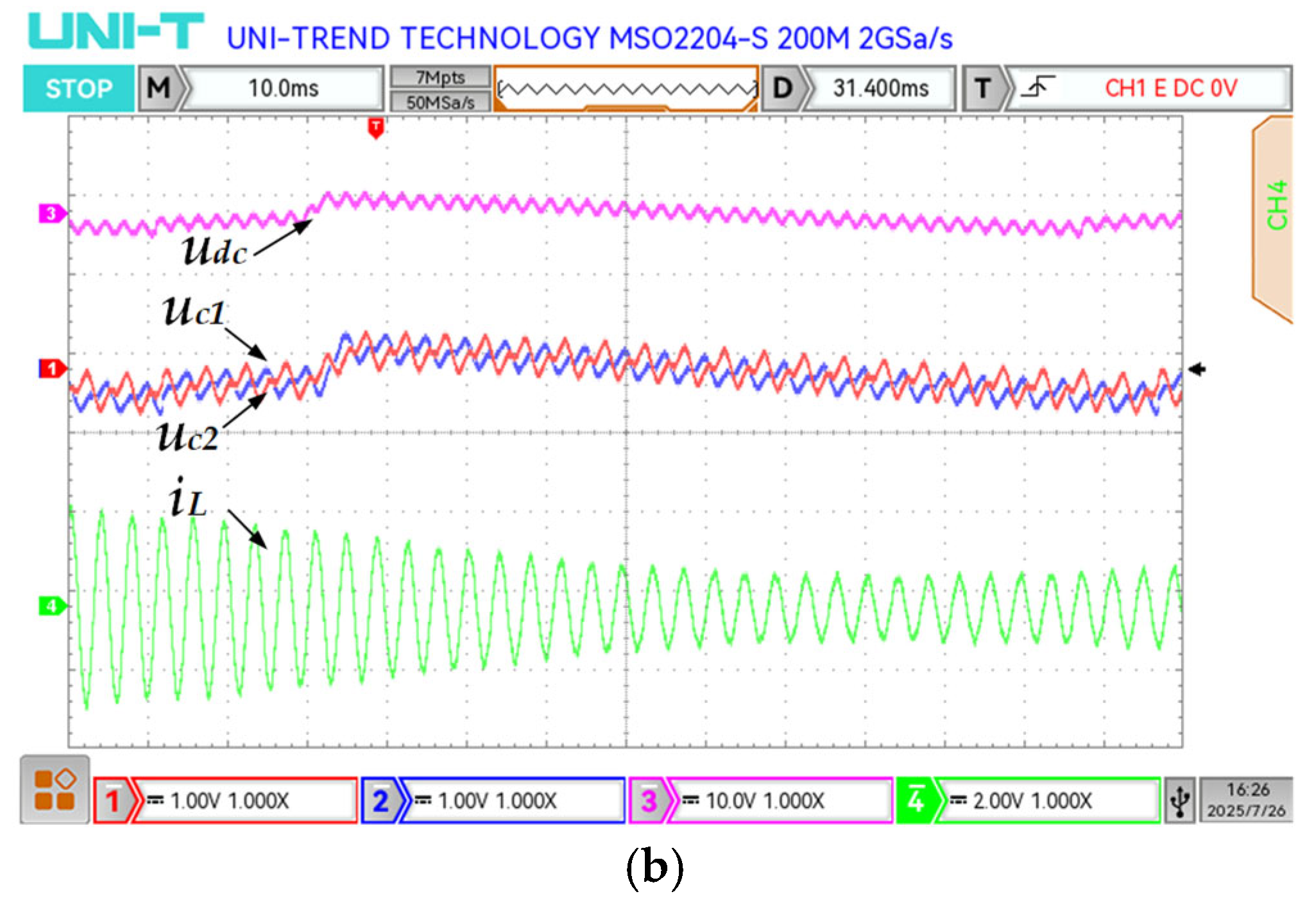
The experimental results of the proposed topology operating in dynamic state are shown in Figure 7, which illustrates the transition between uncontrolled and controlled modes.
Figure 7a,b show that when the load changes, the proposed topology can still achieve power factor correction, and there are only small fluctuations in the DC side voltage. These experimental results demonstrate that the proposed system exhibits good overall performance.
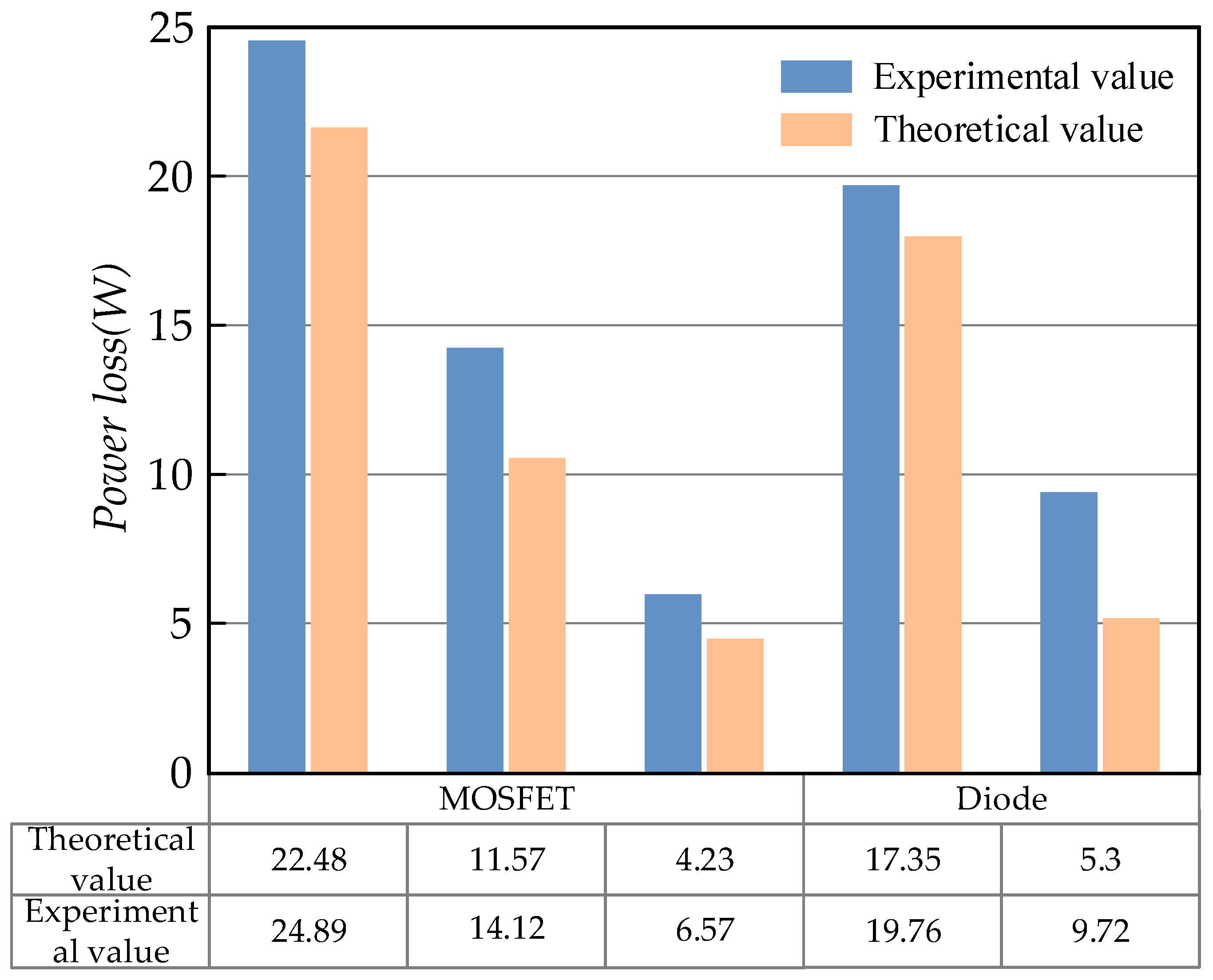
Figure 8 compares the theoretical loss values calculated using the proposed method with the experimental results obtained from the experimental prototype at a rated output of 1 kW. The experimental values are slightly higher than the theoretical values, but the loss trends remain consistent. This difference arises because the theoretical results are obtained from a simplified analytical model that considers only conduction losses and idealized switching losses, in order to keep the derivation concise and highlight the methodological framework. Consequently, parasitic parameters and other non-ideal effects are excluded. In contrast, the experimental models incorporate more realistic device characteristics, which lead to slightly higher calculated switching losses. These deviations are expected and fall within a reasonable range, and they also highlight the gap between idealized models and practical conditions. Overall, the results confirm the feasibility and accuracy of the proposed modal segment integration method for efficiency estimation.
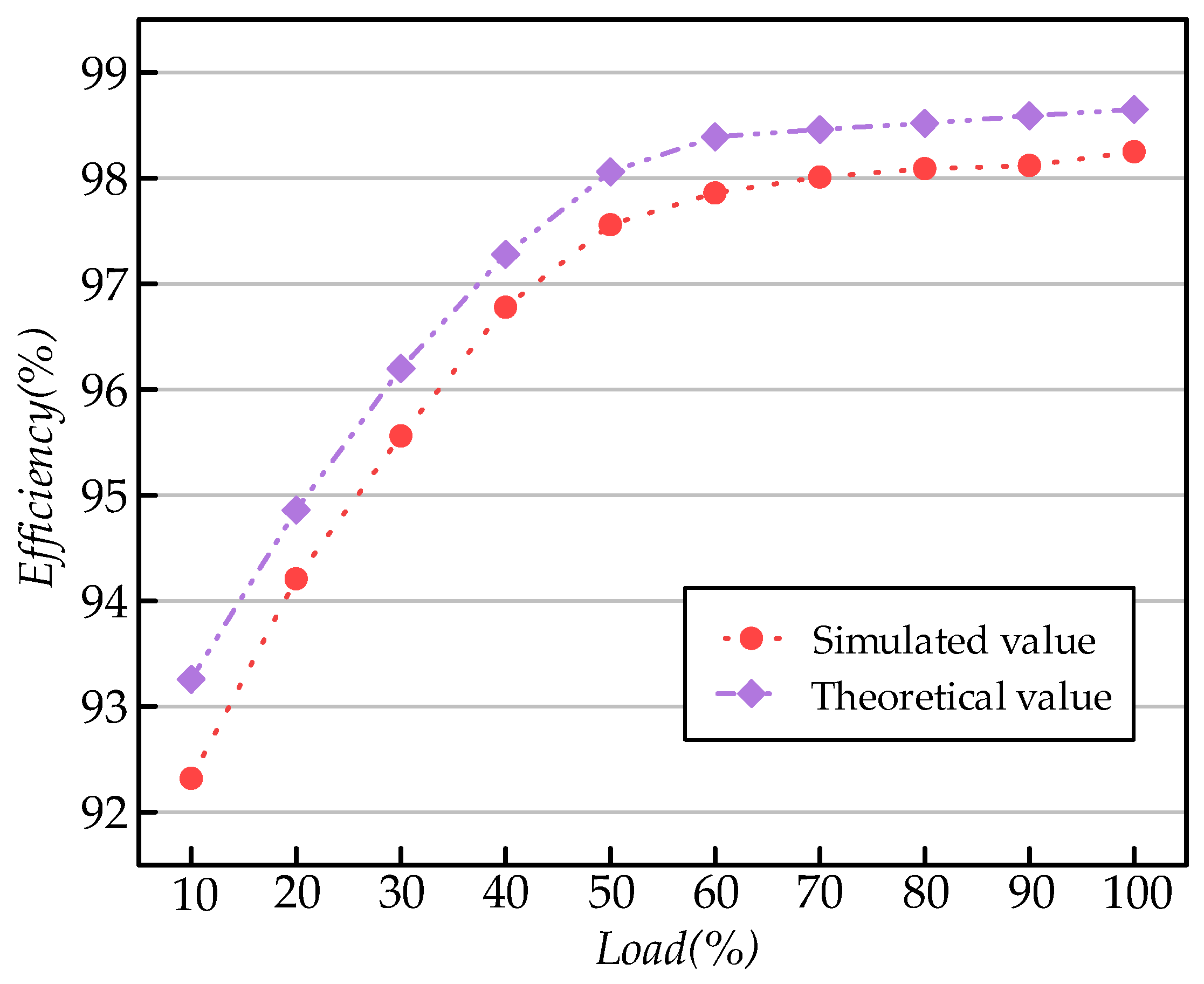
The efficiency of the experimental prototype at different load factors is obtained by adjusting the load ratio. Figure 9 shows the comparison between theoretical efficiency values of the proposed method and simulated efficiency values of the experimental prototype at different load factors.
As shown in Figure 9, the theoretical and simulated values are highly consistent, with a maximum error below 0.4%. The theoretical values are generally higher than the simulated values, which is consistent with the loss comparison in Figure 8, since parasitic effects are not included in the theoretical analysis. Overall, the proposed efficiency analysis method based on the modal segment integration method is highly accurate.

5. Conclusions

To improve upon the traditional efficiency analysis method of bridgeless three-level PFC rectifiers, which relies heavily on simulations and lacks sufficient theory, this paper proposes a modal segment integration method based on a device loss model. First, the operating principle of the proposed topology is analyzed. Then, a power device loss model is constructed and the system efficiency is estimated through modal segment integration method. Finally, the method is verified by using a 1 kW/20 kHz experimental prototype, and the conclusions are as follows:
  • A modal segment integration method based on the device loss model is proposed to estimate the theoretical efficiency of bridgeless three-level PFC rectifier over a complete cycle. This method improves the theoretical basis of the efficiency analysis method and enhances its applicability during the design stage.
  • Simulations and experiments demonstrate that the proposed efficiency estimation method is highly accurate. The error between the theoretical and experimental data is less than 0.4%, which verifies the method’s reliability.
  • The experimental prototype was tested under both steady-state and dynamic operating conditions, and the results confirmed that the proposed topology exhibits excellent power factor correction capability and stable operational performance.
  • In the future, this method can be expanded to the efficiency analysis of multilevel topologies and multiport power conversion systems. The analytical model can also be extended to include parasitic parameters, which would further improve the accuracy of theoretical prediction. In addition, it can be combined with dynamic modeling and intelligent algorithm optimization under complex operating conditions to achieve intelligent and generalized efficiency evaluation.

Author Contributions

Conceptualization, Y.H. and Y.L.; methodology, Y.L. and Z.Y.; validation, Z.Y., Y.L. and Z.C.; formal analysis, Y.L.; investigation, Z.Y.; resources, Z.C.; data curation, Z.Y.; writing—original draft preparation, Z.Y.; writing—review and editing, Z.Y.; visualization, Z.C.; supervision, Y.H. All authors have read and agreed to the published version of the manuscript.

Funding

This research received no external funding.

Data Availability Statement

The original contributions presented in this study are included in the article. Further inquiries can be directed to the corresponding author.

Conflicts of Interest

The authors declare no conflict of interest.

References

  1. Lee, J.-S.; Lee, K.-B. A Novel Carrier-Based PWM Method for Vienna Rectifier with a Variable Power Factor. IEEE Trans. Ind. Electron. 2016, 63, 3–12. [Google Scholar] [CrossRef]
  2. Soeiro, T.B.; Kolar, J.W. Analysis of High-Efficiency Three-Phase Two- and Three-Level Unidirectional Hybrid Rectifiers. IEEE Trans. Ind. Electron. 2013, 60, 3589–3601. [Google Scholar] [CrossRef]
  3. Rodriguez, J.; Lai, J.-S.; Peng, F.Z. Multilevel Inverters: A Survey of Topologies, Controls, and Applications. IEEE Trans. Ind. Electron. 2002, 49, 724–738. [Google Scholar] [CrossRef]
  4. Kolar, J.W.; Friedli, T. The Essence of Three-Phase PFC Rectifier Systems—Part I. IEEE Trans. Power Electron. 2013, 28, 176–198. [Google Scholar] [CrossRef]
  5. Ortmann, M.S.; Mussa, S.A.; Heldwein, M.L. Three-Phase Multilevel PFC Rectifier Based on Multistate Switching Cells. IEEE Trans. Power Electron. 2015, 30, 1843–1854. [Google Scholar] [CrossRef]
  6. Wang, C.; Cheng, B.; He, X.; Xi, L.; Yang, N.; Zhao, Z.; Lai, C.S.; Lai, L.L. Integrated Underfrequency Load Shedding Strategy for Islanded Microgrids Integrating Multiclass Load-Related Factors. IEEE Trans. Smart Grid 2025, 367, 123343. [Google Scholar] [CrossRef]
  7. IEEE Std 519-2022; Standard for Harmonic Control in Electric Power Systems. IEEE: Piscataway, NJ, USA, 2022.
  8. IEC 61000-3-2:2018; Electromagnetic Compatibility (EMC)—Part 3-2: Limits—Limits for Harmonic Current Emissions (Equipment Input Current ≤ 16 A per Phase). International Electrotechnical Commission: Geneva, Switzerland, 2018.
  9. Hartmann, M.; Miniboeck, J.; Ertl, H.; Kolar, J.W. A Three-Phase Delta Switch Rectifier for Use in Modern Aircraft. IEEE Trans. Ind. Electron. 2012, 59, 3635–3647. [Google Scholar] [CrossRef]
  10. Gong, G.; Heldwein, M.L.; Drofenik, U.; Mino, K.; Kolar, J.W. Comparative Evaluation of Three-Phase High Power Factor AC-DC Converter Concepts for Application in Future More Electric Aircrafts. In Proceedings of the Nineteenth Annual IEEE Applied Power Electronics Conference and Exposition, 2004. APEC ’04., Anaheim, CA, USA, 22–26 February 2004; Volume 2, pp. 1152–1159. [Google Scholar]
  11. Siu, K.K.M.; Ho, C.N.M. Manitoba Rectifier—Bridgeless Buck–Boost PFC. IEEE Trans. Power Electron. 2020, 35, 403–414. [Google Scholar] [CrossRef]
  12. Perez-Tarragona, M.; Sarnago, H.; Lucia, O.; Burdio, J.M. Multiphase PFC Rectifier and Modulation Strategies for Domestic Induction Heating Applications. IEEE Trans. Ind. Electron. 2021, 68, 6424–6433. [Google Scholar] [CrossRef]
  13. Al-Saffar, M.A.; Ismail, E.H.; Sabzali, A.J. Integrated Buck–Boost–Quadratic Buck PFC Rectifier for Universal Input Applications. IEEE Trans. Power Electron. 2009, 24, 2886–2896. [Google Scholar] [CrossRef]
  14. Kim, J.-S.; Lee, S.-H.; Cha, W.-J.; Kwon, B.-H. High-Efficiency Bridgeless Three-Level Power Factor Correction Rectifier. IEEE Trans. Ind. Electron. 2017, 64, 1130–1136. [Google Scholar] [CrossRef]
  15. Lange, A.D.B.; Soeiro, T.B.; Ortmann, M.S.; Heldwein, M.L. Three-Level Single-Phase Bridgeless PFC Rectifiers. IEEE Trans. Power Electron. 2015, 30, 2935–2949. [Google Scholar] [CrossRef]
  16. Ma, H.; Zheng, K.; Jiang, H.; Yin, H. A Family of Dual-Boost Bridgeless Five-Level Rectifiers with Common-Core Inductors. IEEE Trans. Power Electron. 2021, 36, 12565–12578. [Google Scholar] [CrossRef]
  17. Lee, Y.-D.; Kim, D.; Choi, S.-H.; Moon, G.-W.; Kim, C.-E. New Bridgeless Power Factor Correction Converter with Simple Gate Driving Circuit and High Efficiency for Server Power Applications. IEEE Trans. Power Electron. 2020, 35, 13148–13156. [Google Scholar] [CrossRef]
  18. Meng, T.; Ben, H.; Li, C.; Wei, G. Investigation and Implementation of a Passive Snubber with a Coupled-Inductor in a Single-Stage Full-Bridge Boost PFC Converter. J. Power Electron. 2013, 13, 206–213. [Google Scholar] [CrossRef]
  19. Chen, J.-F.; Chen, R.-Y.; Liang, T.-J. Study and Implementation of a Single-Stage Current-Fed Boost PFC Converter with ZCS for High Voltage Applications. IEEE Trans. Power Electron. 2008, 23, 379–386. [Google Scholar] [CrossRef]
  20. Hu, Y.; Huber, L.; Jovanović, M.M. Single-Stage, Universal-Input AC/DC LED Driver With Current-Controlled Variable PFC Boost Inductor. IEEE Trans. Power Electron. 2012, 27, 1579–1588. [Google Scholar] [CrossRef]
  21. Cao, J.; Pei, Y.; Wang, Z. Analysis of Power Dissipation of Switching Components in Boost PFC Circuit. Adv. Technol. Electr. Eng. Energy 2002, 21, 41–44. [Google Scholar]
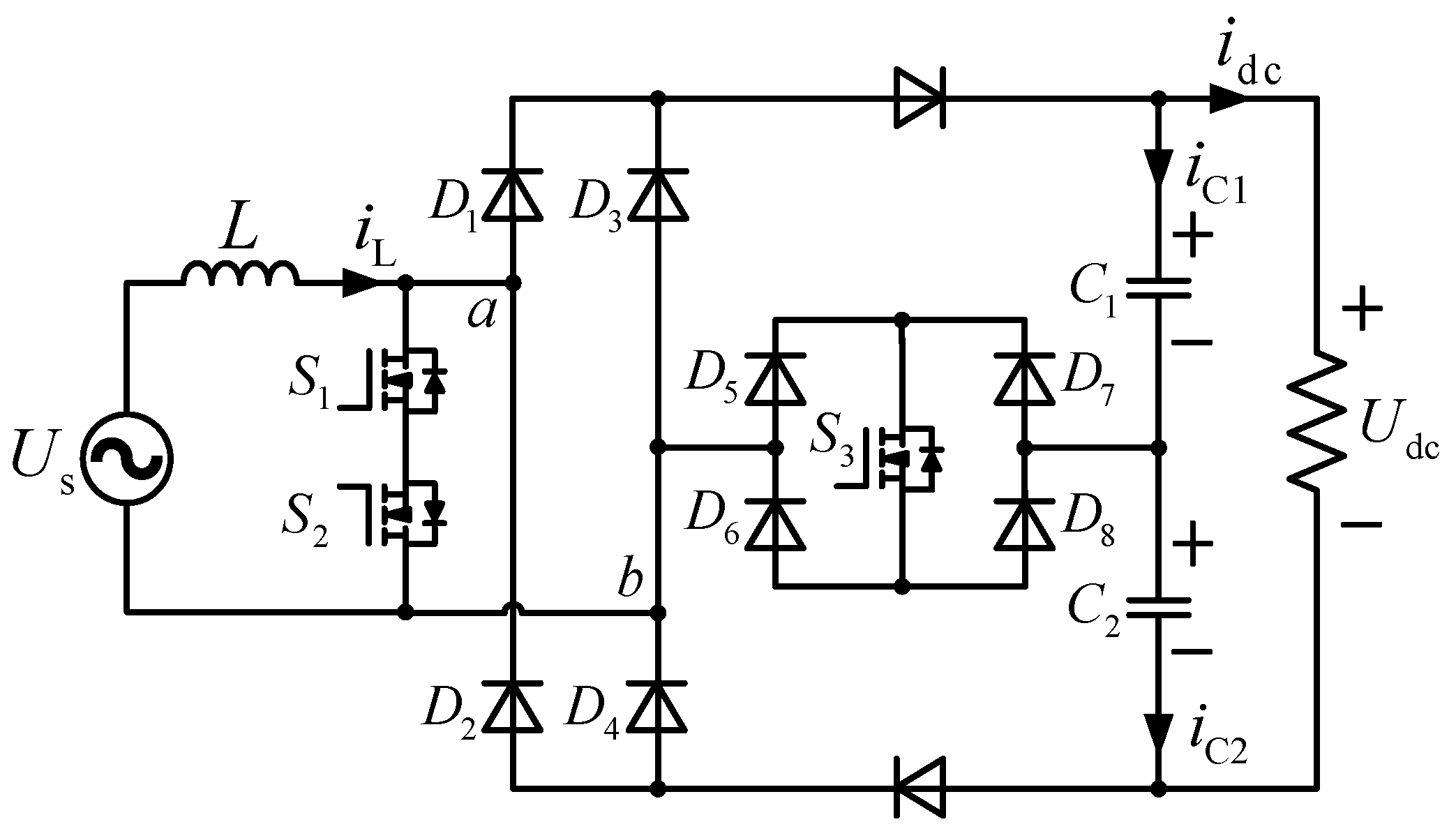
Figure 1. New three−level PFC topology.
Electronics 14 03592 g001
Figure 2. Key waveforms of the bridgeless three-level (PFC) circuit in operating mode. (uab is the bridge arm voltage, iL is the input inductance current, and uc1 and uc2 are the voltages of the split capacitors c1 and c2, respectively).
Electronics 14 03592 g002
Figure 3. Analysis of operating modes. (a) Mode 1. (b) Mode 2. (c) Mode 3. (d) Mode 4. (e) Mode 5. (f) Mode 6.
Electronics 14 03592 g003aElectronics 14 03592 g003b
Figure 4. Distribution of power loss at rated power.
Electronics 14 03592 g004
Figure 5. Experimental prototype.
Electronics 14 03592 g005
Figure 6. The steady-state waveforms of the proposed topology. (a) The pulse distribution waveforms. (b) The input voltage uab. (c) The voltage waveforms.
Electronics 14 03592 g006aElectronics 14 03592 g006b
Figure 7. The dynamic waveforms of the proposed topology. (a) Step−up of load. (b) Step−down of load.
Electronics 14 03592 g007aElectronics 14 03592 g007b
Figure 8. Theoretical vs. experimental losses of power switching devices at 1 kW operating conditions.
Electronics 14 03592 g008
Figure 9. Efficiency comparison chart.
Electronics 14 03592 g009
Table 1. Voltage stress on switching devices.
Switching DeviceVoltage Stress
S1Udc
S2Udc
S3Udc/2
D1–D4Udc
D5, D6Udc/2
D7, D8Udc/2
Table 2. Experimental parameters.
ParametersValue
Input AC voltage220 V
Output DC voltage400 V
Rated output power1 kW
Switching frequency20 kHz
Input inductor2.5 mH
Split DC-link capacitor2000 μF
Disclaimer/Publisher’s Note: The statements, opinions and data contained in all publications are solely those of the individual author(s) and contributor(s) and not of MDPI and/or the editor(s). MDPI and/or the editor(s) disclaim responsibility for any injury to people or property resulting from any ideas, methods, instructions or products referred to in the content.