Article

Impact of Grain Boundaries on Zero-Temperature Coefficient Characteristics in a 3D-Stacked Transistor

1
Department of Electronics Engineering, Gyeongkuk National University, Andong 36729, Republic of Korea
2
School of Electronic and Electrical Engineering, Kyungpook National University, Daegu 41566, Republic of Korea
3
School of Electronic and Mechanical Engineering, Gyeongkuk National University, Andong 36729, Republic of Korea
4
Department of Electronic Engineering, Soonchunhyang University, Asan 31538, Republic of Korea
*
Authors to whom correspondence should be addressed.
Electronics 2025, 14(17), 3494; https://doi.org/10.3390/electronics14173494
Submission received: 8 August 2025 / Revised: 29 August 2025 / Accepted: 30 August 2025 / Published: 31 August 2025

Abstract

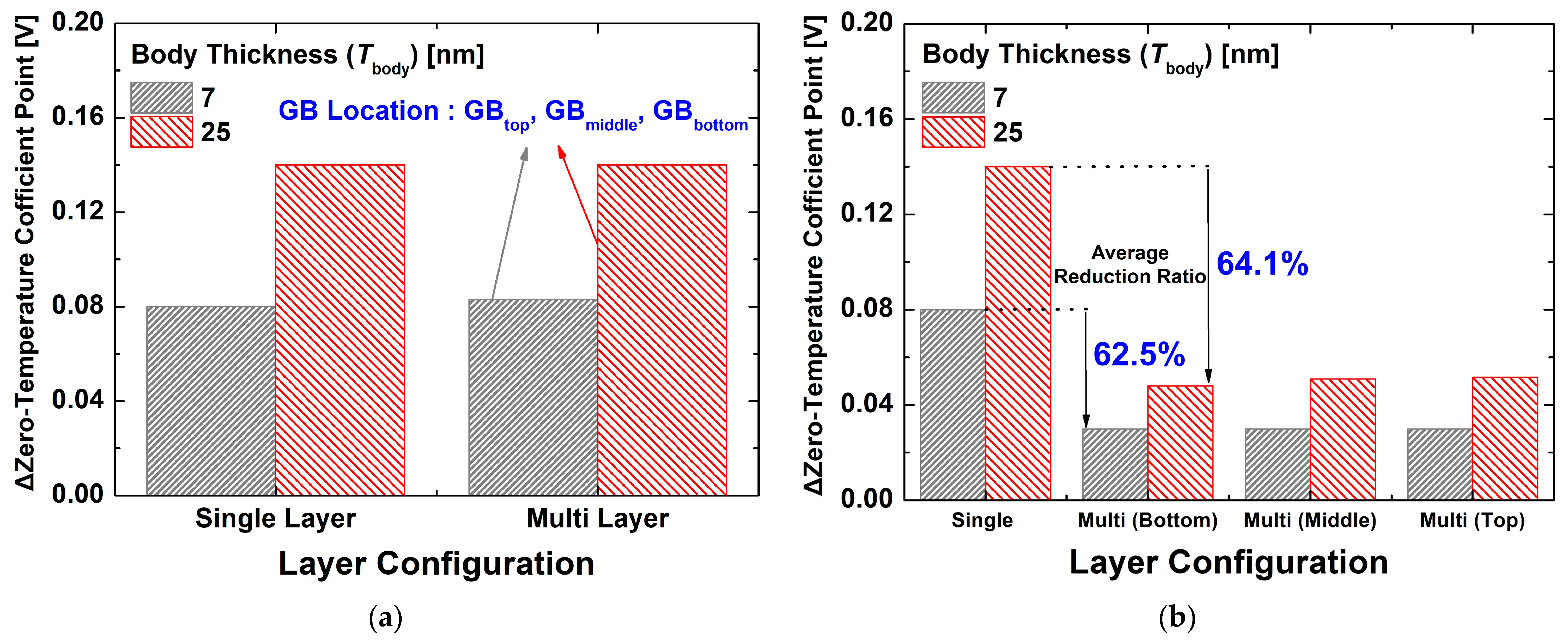
In this paper, we investigate the zero-temperature coefficient (ZTC) characteristics of polycrystalline silicon (poly-Si) single-gate transistors with a silicon-on-insulator (SOI)-like structure, which offers thermal stability over a wide temperature range. While ZTC characteristics have been primarily utilized in analog and memory circuits, systematic analyses for logic transistors remain limited. The ZTC characteristic is quantitatively evaluated by considering various process parameters, including high-density three-dimensional (3D)-stacked structures. The effects of grain boundary (GB) location within the poly-Si, body thickness, and doping concentration on both the ZTC point and its temperature sensitivity are systematically analyzed. A new metric, ΔZTC, is defined to quantify the sensitivity of the ZTC point to the presence or absence of GBs. This metric is applied throughout the analysis. As a result, ZTC characteristics can be effectively optimized through structural parameter adjustment, and these characteristics are maintained or even enhanced when extended to multi-layer architectures. Notably, when GBs are confined to specific layers, the ΔZTC value is reduced by approximately 64.1% at a body thickness of 25 nm and by 62.5% at 7 nm, compared to the single-layer structure, indicating that temperature sensitivity can be significantly suppressed.

1. Introduction

With rapid advancements in the performance and integration density of modern logic integrated circuits, ensuring stable electrical characteristics of devices under varying temperature conditions has become a critical design consideration [1,2,3,4,5,6]. As technology scaling continues, the increasing temperature sensitivity of current characteristics may become a major cause of circuit malfunction. One approach to solve this issue is to utilize the zero-temperature coefficient (ZTC) characteristic, where the drain current remains nearly unaffected by temperature variations under specific gate bias conditions [7,8,9,10]. While ZTC characteristics have been primarily utilized in temperature-compensated analog and memory circuit designs, systematic analysis and design parameter optimization in logic transistors have remained limited [11,12,13]. Furthermore, although widely studied in conventional single-crystal silicon transistors, the application of these characteristics to polycrystalline silicon (poly-Si) devices, which are important for 3D integration, has not been fully established. The inherent grain boundaries (GBs) in poly-Si can introduce variability and pose a notable challenge when achieving stable ZTC behavior. In this study, the ZTC characteristics of poly-Si single-gate transistors with a silicon-on-insulator (SOI)-like structure are investigated. This structure offers structural advantages that are well-suited for high-density three-dimensional (3D) integration. It also reflects realistic, process-dependent physical properties, such as the grain boundaries (GBs) inherent in polycrystalline silicon, indicating its potential applicability for next-generation logic devices like monolithic 3D (M3D) integrated circuits and advanced memory like 3D NAND flash [14,15,16,17,18,19,20,21,22,23,24,25,26,27,28,29,30]. To quantitatively analyze the impact of GBs, we utilize the ZTC variation (ΔZTC) as a practical figure of merit. Sentaurus TCAD simulation is used to analyze the IV characteristics under various temperature conditions, and the ZTC point is quantitatively extracted using doping concentration and channel thickness as key design variables [31]. Based on this analysis, the thermal stability of the proposed structure is evaluated, along with its extensibility from a single-gate device to a 3D-stacked configuration. Logic devices with improved temperature stability can maintain reliable electrical performance even in 3D integration environments, serving as a foundation for highly integrated and thermally stable logic circuit design.

2. Device Structure and Simulation Method

Figure 1a shows a cross-sectional view of the poly-Si-based single-gate transistor structure. The source and drain regions are composed of poly-Si (n-type), while the body region is formed using poly-Si (p-type). The gate dielectric is made of HfO2, providing electrical insulation from the channel. In addition, spacer dielectrics composed of SiO2 are formed at both ends of the device, helping electrically isolate the gate and adjacent devices.
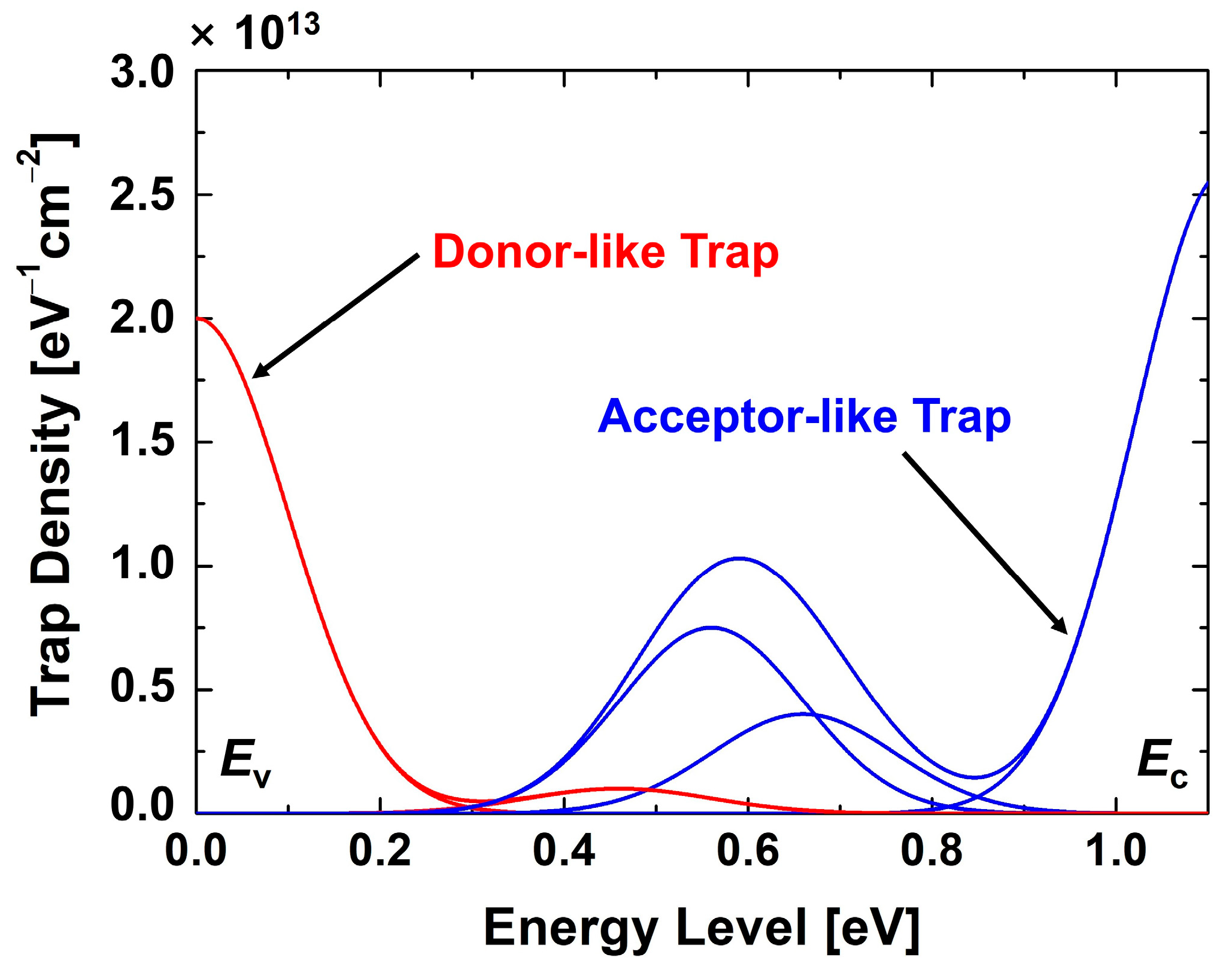
Figure 1b shows the positions of GBs within the body region. In the TCAD simulations, the gate length was fixed at 70 nm, a representative technology node, because ZTC characteristics can be highly sensitive to short-channel effects. This setup allowed the effects of body thickness and doping concentration to be analyzed independently in a controlled environment. Under these conditions, three−GB positions were defined in the poly-Si transistor to evaluate their impact on ZTC behavior. The GBs were placed 7 nm from the source junction (x = 7 nm), at the channel center (x = 35 nm), and near the drain junction (x = 63 nm), reflecting distributions that can occur in actual fabrication processes. These settings were intended to systematically examine how GBs influence charge transport and trapping phenomena. Table 1 summarizes the key parameters used in the simulations. The gate length (Lg) was set to 70 nm, and the body thickness (Tbody) varied from 7 to 25 nm in 2 nm increments to examine its effect on device characteristics. The gate oxide thickness (Tox) was set to 3 nm to meet the equivalent oxide thickness requirement specified by the International Roadmap for Devices and Systems (IRDS) [32]. The doping concentration for the source and drain regions was 5 × 1019 cm−3 (n-type), and the body region was doped with a concentration ranging from 1 × 10¹⁶ to 1 × 1018 cm−3 (p-type). Based on these parameters, the Sentaurus TCAD simulation was used to analyze the impact of GBs on the ZTC point. The GB was modeled as a two-dimensional interface plane rather than as a region with physical thickness. To replicate the electrical characteristics of the GB, Gaussian-distributed trap states were assigned to this interface to simulate carrier trapping phenomena, as illustrated in Figure 2. Considering the device’s channel length, it is expected that at most one GB would be present within the channel. Therefore, the analysis focused on evaluating how the device’s characteristics are influenced when a GB is located at different critical positions along the channel. To ensure accurate electrical characterization, mobility, Shockley–Read–Hall recombination, Auger recombination, band-to-band tunneling, and quantum potential models were applied.

3. Results and Discussion

3.1. Characteristics of Single-Layer Device

Figure 3 shows the transfer characteristics of a single-layer device at various temperatures (300–400 K), simulated under different body doping concentrations and grain boundary (GB) conditions. The ZTC point, defined as the gate voltage at which the increase in drain current due to the reduction in threshold voltage (Vth) is balanced by the decrease caused by mobility ( μ ) degradation, was identified within this temperature range.
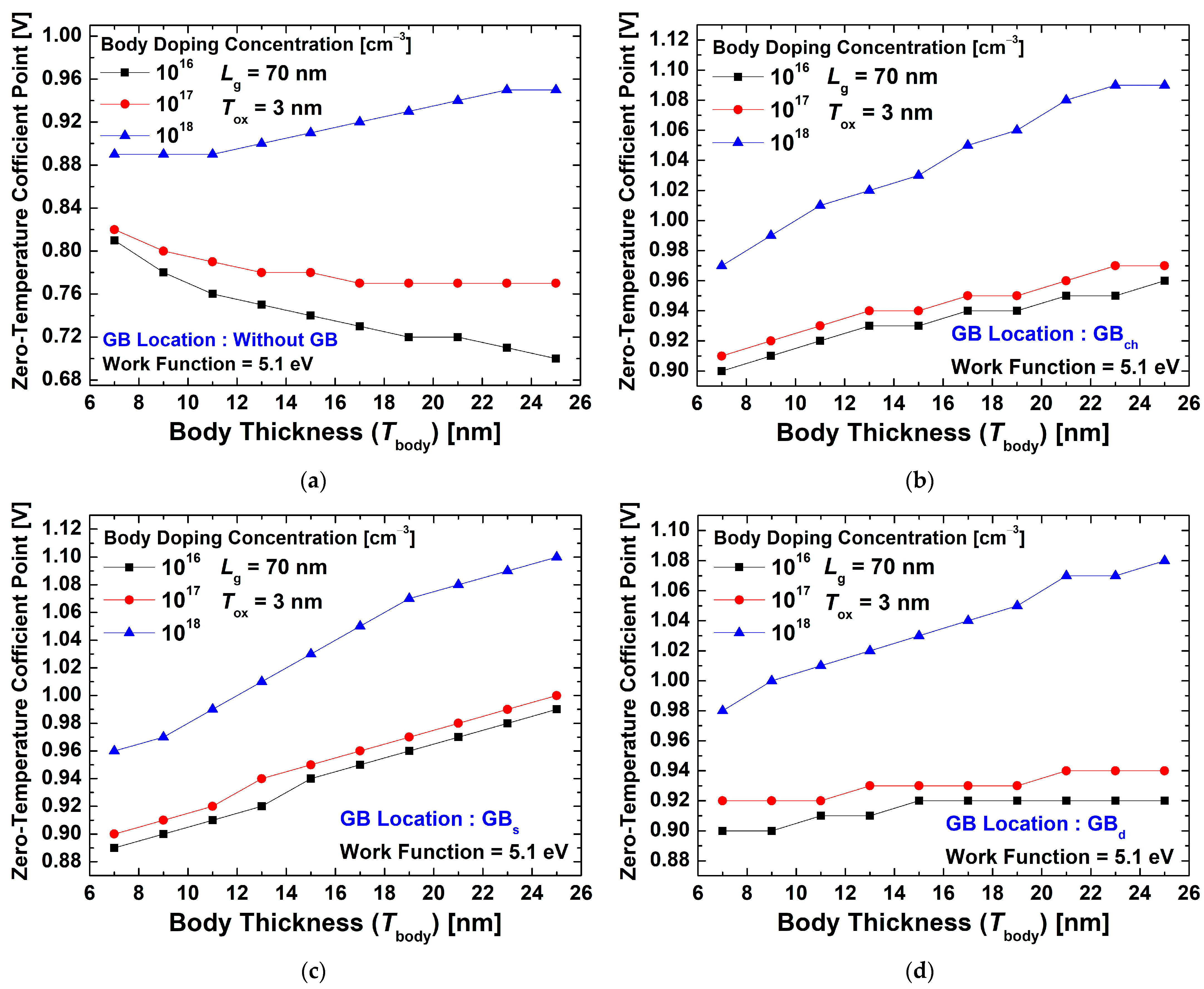
The variation in the ZTC point as a function of body thickness in the absence of GBs is shown in Figure 4a. When the body doping concentration is 1 × 1016 cm−3 or 1 × 1017 cm−3, the ZTC point decreases as the body thickness increases. In contrast, at a high doping concentration of 1 × 1018 cm−3, the ZTC point increases with increasing body thickness. This opposite trend arises because the temperature dependence of mobility and threshold voltage, both of which influence the temperature characteristics of current, act differently depending on the doping concentration. Under low doping conditions, the temperature dependence of mobility has a more dominant impact on current variation, and the increased body thickness further degrades mobility, resulting in a lower ZTC point [33]. In contrast, under high doping conditions, the temperature dependence of threshold voltage plays a more critical role. As the body becomes thicker, changes in threshold voltage are more directly reflected in the drain current, resulting in an increase in the ZTC point [34].
Figure 4b–d show the variation in the ZTC point as a function of body thickness when the GB is located at the channel center, source side, and drain side, respectively. When GBs are present, the ZTC point increases with body thickness under all doping conditions. This phenomenon is attributed to variation in the temperature dependence of the Vth caused by potential barriers formed through charge trapping at the GB. In thin-body devices, the charge trapping effect induced by the GB strongly influences the entire channel, leading to greater variations in Vth with temperature. In contrast, as the body thickness increases, the trapped charges are more spatially distributed throughout the body, mitigating the influence of the GB-induced potential barrier and thereby reducing the temperature dependence of Vth. Consequently, the ZTC point shifts toward higher gate voltages as the body becomes thicker [18,19].
The doping concentration directly affects both the magnitude of the GB-induced potential barrier and its temperature dependence. At lower doping concentrations, the potential barrier exhibits higher temperature sensitivity, resulting in the formation of the ZTC point at a lower gate voltage, which gradually increases with body thickness. At higher doping concentrations, the ZTC point appears at a fundamentally higher gate voltage and shows a more pronounced increase as the body thickness increases [20].
The preceding analysis revealed that the ZTC point varies depending on the location of the GB. However, evaluating the quantitative impact of GBs on the device’s temperature characteristics based solely on the ZTC point remains challenging. Therefore, in this study, the concept of the ZTC variation (ΔZTC) is introduced to analyze the difference in ZTC points with and without the presence of GBs.
The ZTC variation (ΔZTC) is defined as follows:
Z T C = Z T C w i t h   G B Z T C w i t h o u t   G B
ZTC with GB refers to the ZTC point when a GB is present at a specific location, whereas ZTC without GB represents the ZTC point under the same conditions without the presence of a GB. A larger ΔZTC value indicates a greater impact of the GB, while a smaller value suggests a lesser influence. This metric allows for the quantitative comparison of ZTC sensitivity with respect to GB location, body thickness, and doping concentration.
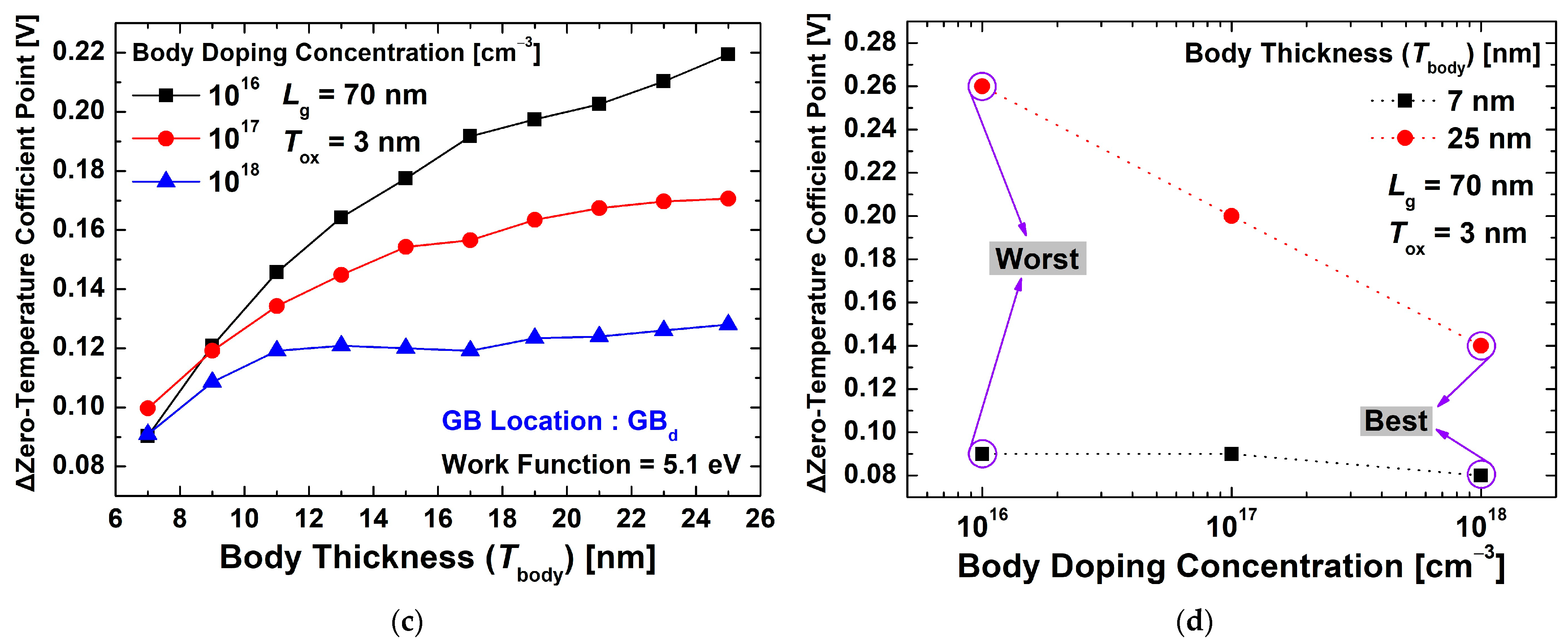
In Figure 5a–c, the ΔZTC is shown as a function of body thickness and doping concentration when the GB is located at the channel center, source side, and drain side, respectively. For all GB locations, ΔZTC increases with body thickness regardless of doping concentration. This indicates that the impact of the GB on the device’s temperature characteristics becomes more significant as the body becomes thicker. A larger ΔZTC value means a greater difference in the ZTC point due to the presence of a GB, whereas a smaller ΔZTC value indicates a smaller influence of the GB.
Figure 5d shows ΔZTC as a function of doping concentration for two body thicknesses, 7 nm and 25 nm, under the condition where the GB is located at the center of the channel. Since the channel region serves as the main conduction path for electrons, the presence of a GB in this location has the most significant impact on the device’s temperature characteristics. Therefore, the condition with the GB at the channel center is used as the reference, and for each body thickness, the highest and lowest ΔZTC values are defined as the worst and best cases, respectively.
ΔZTC tends to increase at lower doping concentrations, and this effect is particularly pronounced at a body thickness of 25 nm, where the ΔZTC reaches its maximum at a doping level of 1 × 1016 cm−3, making it the worst case for this thickness. Conversely, increasing the doping concentration to 1 × 1018 cm−3 significantly reduces ΔZTC, thereby representing the best case. Likewise, for the thinner 7 nm body, ΔZTC is relatively larger at lower doping levels and minimized at higher doping levels. These results indicate that the impact of GBs on temperature-dependent characteristics varies significantly depending on the combination of body thickness and doping concentration. By optimizing these conditions, the influence of GBs can be effectively suppressed, thereby enhancing the thermal stability of the device.

3.2. Characteristics of Multi-Layer Device

In the previously discussed single-layer structure, the thermal stability of the device was analyzed with a focus on the ZTC characteristics depending on the GB location. In this section, the analysis is extended to a vertically stacked multi-layer configuration to quantitatively evaluate the impact of GBs in such structures and to explore structural optimization strategies for minimizing their influence.
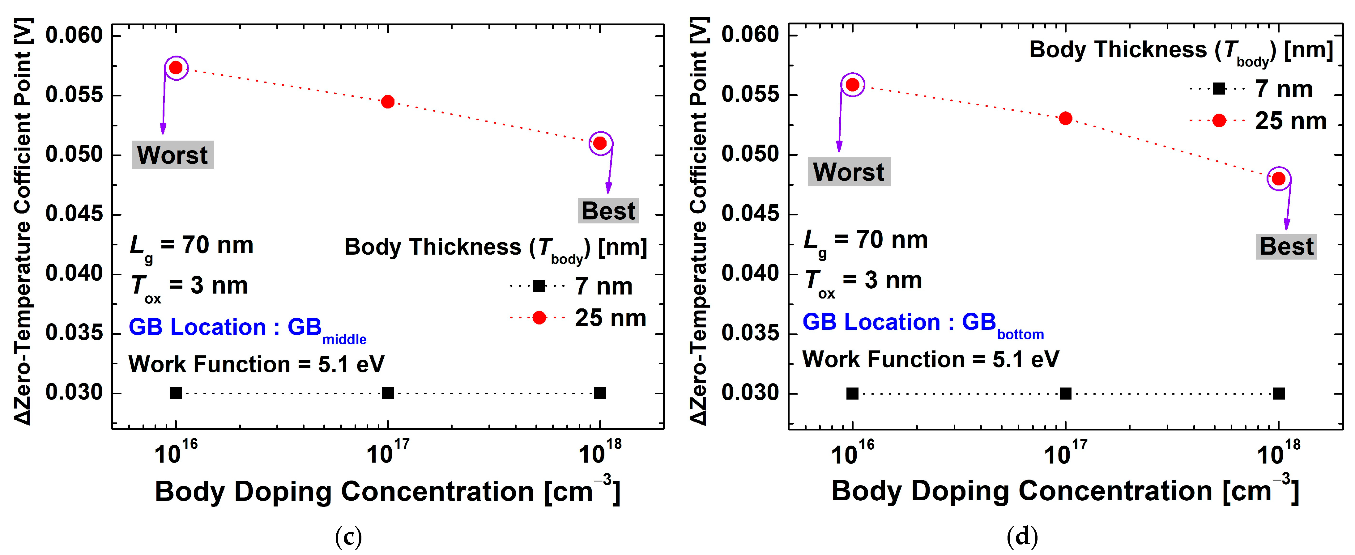
Figure 6a shows the cross-sectional view of a multi-layer transistor structure, constructed by vertically stacking the previously discussed single-layer devices. This structure is based on the same device configuration and process conditions, and all parameters applied are identical to those listed for the single-layer case in Table 1. As shown in Figure 6b, the structural model assumes the GB to be located at the top, middle, or bottom of each layer. Among these, only the condition where the GB is placed at the center of the channel is considered, since the channel is the primary conduction path for electrons, and a GB at this location directly affects the temperature-dependent characteristics. As in the single-layer case, the impact of GBs was evaluated by defining the case with the largest ΔZTC as the worst condition and the one with the smallest as the best.
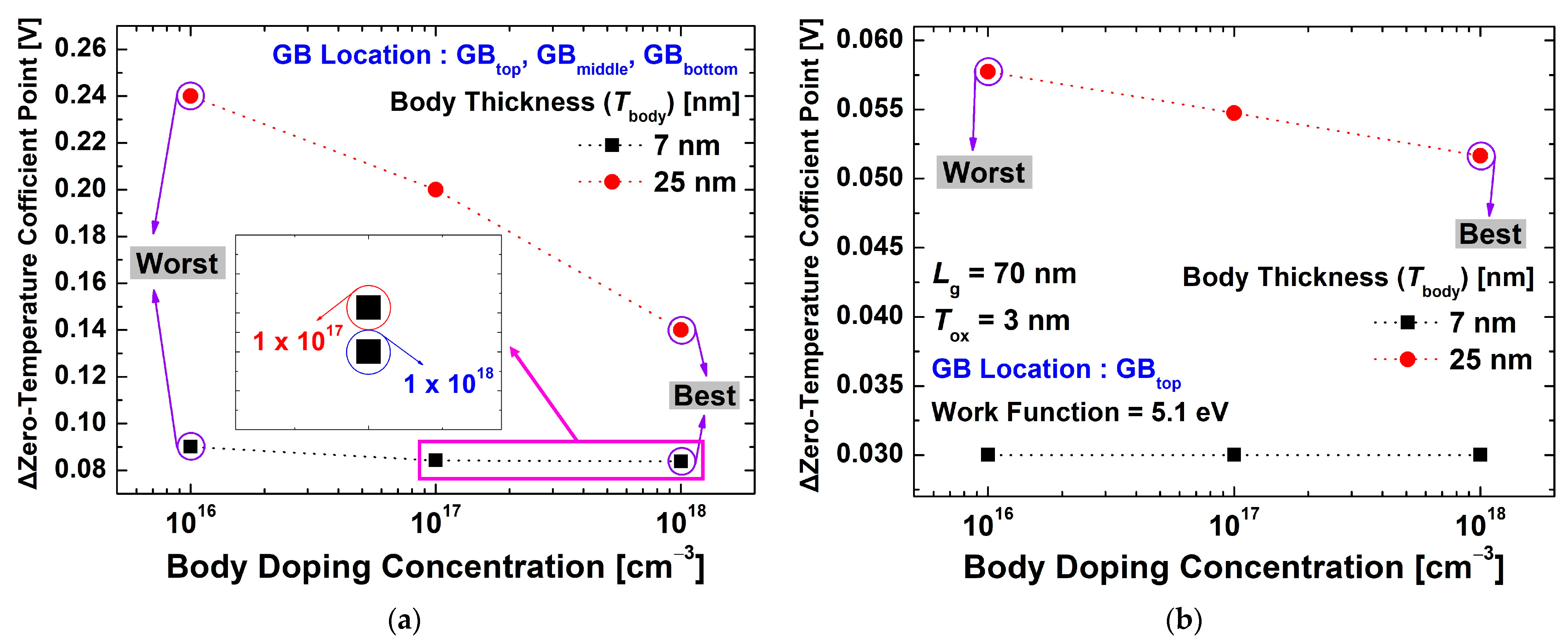
Figure 7a shows the ΔZTC characteristics when GBs are present in all three layers (top, middle, and bottom) of the multi-layer structure. Regardless of body thickness, ΔZTC exhibits its highest value at low doping concentrations and its lowest at high doping concentrations. A single GB is assumed to be located in only one of the three layers: top, middle, or bottom. The resulting ΔZTC characteristics for each condition are shown in Figure 7b–d. In all three cases, similar trends are observed. When the body thickness is 7 nm, ΔZTC remains consistently low regardless of doping concentration. In contrast, for a body thickness of 25 nm, ΔZTC varies significantly with doping concentration, showing the highest value at low doping and gradually decreasing as the doping level increases.
These results indicate that the combination of thin body thickness and high doping concentration offers the most favorable conditions in terms of ΔZTC characteristics, suggesting an optimal configuration for ensuring thermal stability even in the presence of GBs. Furthermore, compared to a single-layer structure under the same conditions, the multi-layer configuration consistently exhibits lower ΔZTC values. This implies that the multi-layer structure can more effectively suppress the impact of GBs, thereby serving as a promising design strategy for enhancing thermal stability and electrical reliability in 3D stacked devices.
Figure 8 presents a comparative analysis of ΔZTC characteristics as a function of GB location in both single-layer and multi-layer structures, serving as a critical internal benchmark that underscores the advantages of the multi-layer configuration. For the single-layer structure, only the condition in which the GB is located at the center of the channel was considered for comparison. Figure 8a compares the case where GBs are present in all layers (top, middle, and bottom) of a multi-layer structure with that of a single-layer structure. The ΔZTC value is highest when the body thickness is 25 nm and lowest at 7 nm. Notably, in the multi-layer structure, even though GBs exist simultaneously in all layers, the ΔZTC value remains nearly identical to that of the single-layer case, indicating that the influence of GBs can be effectively suppressed. Figure 8b shows the comparison results when a GB exists in only one of the layers. Compared to the single-layer structure, a reduction in ΔZTC is observed. Specifically, an average reduction of approximately 64.1% is seen at a body thickness of 25 nm, and about 62.5% at 7 nm, suggesting that the multi-layer structure serves as a favorable design option for improving the stability of ΔZTC characteristics.

4. Conclusions

This study analyzed how GB location, body thickness, and doping concentration influence ZTC characteristics of single-layer and multi-layer transistor structures. To measure the effect of GBs on temperature-dependent behavior, we introduced the metric ΔZTC, which quantifies the sensitivity of ZTC shifts. In single-layer devices, ΔZTC was improved by adjusting body thickness and doping concentration. The same optimization pattern appeared in the multi-layer configuration, indicating that the design principles scale across structures. A notable finding was that, when a GB in the multi-layer structure was limited to one layer, ΔZTC dropped significantly compared with the single-layer case. These results point to a practical strategy for reducing GB-related temperature sensitivity in both types of devices and for improving the thermal reliability of polycrystalline-based logic circuits. Our analysis focused on a single, well-defined GB to clearly separate positional effects from other variables. Parasitic effects were excluded to better isolate the intrinsic device physics. Key parameters, such as GB trap density, were fixed at a representative value. It would be valuable for future studies to consider incorporating random GB distributions, parasitic effects, and variations in trap density, potentially strengthening the strategy’s robustness and applicability to diverse device designs.

Author Contributions

Conceptualization, K.H.K. and Y.J.Y.; investigation, K.H.K.; data curation, K.H.K.; validation, K.H.K., K.K. and I.M.K.; writing—original draft preparation, K.H.K.; writing—review and editing, K.K. and Y.J.Y. All authors have read and agreed to the published version of the manuscript.

Funding

This work was supported by the Soonchunhyang University Research Fund (No. 20240771). The EDA tool was supported by the IC Design Education Center (IDEC), Korea. This work was also supported by a Research Grant of Gyeongkuk National University.

Data Availability Statement

Data are contained within the article.

Conflicts of Interest

The authors declare no conflicts of interest.

References

  1. Okhonin, S.; Nagoga, M.; Sallese, J.M.; Fazan, P. A capacitor-less 1T-DRAM cell. IEEE Electron. Device Lett. 2002, 23, 85–87. [Google Scholar] [CrossRef]
  2. Mukhopadhyay, S.; Raychowdhury, A.; Roy, K. Accurate estimation of total leakage current in scaled CMOS logic circuits based on compact current modeling. In Proceedings of the 2003 Design Automation Conference (DAC), Anaheim, CA, USA, 2–6 June 2003; pp. 169–174. [Google Scholar] [CrossRef]
  3. Abbas, Z.; Olivieri, M. Impact of technology scaling on leakage power in nano-scale bulk CMOS digital standard cells. Microelectron. J. 2014, 45, 179–195. [Google Scholar] [CrossRef]
  4. Seo, J.H.; Yoon, Y.J.; Yu, E.; Sun, W.; Shin, H.; Kang, I.M.; Lee, J.-H.; Cho, S. Fabrication and Characterization of a Thin-Body Poly-Si 1T DRAM with Charge-Trap Effect. IEEE Electron. Device Lett. 2019, 40, 566–569. [Google Scholar] [CrossRef]
  5. Lee, S.H.; Yoon, Y.J.; Seo, J.H.; Cho, M.S.; Park, J.; An, H.D.; Min, S.R.; Kim, G.U.; Kang, I.M. Effect of Work-function Variation on Transfer Characteristics and Memory Performances for Gate-all-around JLFET based Capacitorless DRAM. J. Semicond. Technol. Sci. 2021, 21, 381–389. [Google Scholar] [CrossRef]
  6. Bae, J.-H.; Back, J.-W.; Kwon, M.-W.; Seo, J.H.; Yoo, K.; Woo, S.Y.; Park, K.; Park, B.-G.; Lee, J.-H. Characterization of a Capacitorless DRAM cell for Cryogenic Memory Applications. IEEE Electron. Device Lett. 2019, 40, 1614–1617. [Google Scholar] [CrossRef]
  7. Prijić, Z.D.; Dimitrijev, S.S.; Stojadinović, N.D. The determination of zero temperature coefficient point in CMOS transistors. Microelectron. Reliab. 1992, 32, 769–773. [Google Scholar] [CrossRef]
  8. Osman, A.A.; Osman, M.A.; Dogan, N.S.; Imam, M.A. Zero-temperature-coefficient biasing point of partially depleted SOI MOSFET’s. IEEE Trans. Electron. Devices 1995, 42, 1709–1711. [Google Scholar] [CrossRef]
  9. Camillo, L.M.; Martino, J.A.; Simoen, E.; Claeys, C. The temperature mobility degradation influence on the zero temperature coefficient of partially and fully depleted SOI MOSFETs. Microelectron. J. 2006, 37, 952–957. [Google Scholar] [CrossRef]
  10. Tan, T.H.; Goel, A.K. Zero-temperature-coefficient biasing point of a fully-depleted SOI MOSFET. Microw. Opt. Technol. Lett. 2003, 37, 366–370. [Google Scholar] [CrossRef]
  11. Kim, K.H.; Kim, K.M.; Kim, Y.H.; Im, J.B.; Choi, G.H.; Kang, I.M.; Yoon, Y.J. Design Optimization of Capacitor-less DRAM using zero-temperature coefficient point. J. Inst. Korean Electr. Electron. Eng. 2024, 28, 369–374. [Google Scholar] [CrossRef]
  12. Kim, K.H.; Kim, K.M.; Kim, Y.H.; Im, J.B.; Choi, G.H.; Kang, I.M.; Yoon, Y.J. Optimization of One-transistor (1T) DRAM using Device Parameters-dependent Zero-temperature Coefficient Point. J. Semicond. Technol. Sci. 2025, 25, 274–283. [Google Scholar] [CrossRef]
  13. Wenger, Y.; Meinerzhagen, B. Low-Voltage Current and Voltage Reference Design Based on the MOSFET ZTC Effect. IEEE Trans. Circuits Syst. I Regul. Pap. 2019, 66, 3445–3456. [Google Scholar] [CrossRef]
  14. Cho, M.S.; Mun, H.J.; Lee, S.H.; Jang, J.; Bae, J.-H.; Kang, I.M. Simulation of capacitorless dynamic random access memory based on junctionless FinFETs using grain boundary of polycrystalline silicon. Appl. Phys. A 2020, 126, 943. [Google Scholar] [CrossRef]
  15. Lee, S.H.; Jang, W.D.; Yoon, Y.J.; Seo, J.H.; Mun, H.J.; Cho, M.S.; Jang, J.; Bae, J.-H.; Kang, I.M. Polycrystalline-Silicon-MOSFET-Based Capacitorless DRAM with Grain Boundaries and Its Performances. IEEE Access 2021, 9, 50281–50290. [Google Scholar] [CrossRef]
  16. Kim, G.U.; Yoon, Y.J.; Seo, J.H.; Lee, S.H.; Park, J.; Kang, G.E.; Heo, J.H.; Jang, J.; Bae, J.-H.; Lee, S.-H.; et al. Design of a Capacitorless DRAM Based on Storage Layer Separated Using Separation Oxide and Polycrystalline Silicon. Electronics 2022, 11, 3365. [Google Scholar] [CrossRef]
  17. Yoo, S.; Sun, W.; Shin, H. Analysis of a Lateral Grain Boundary for Reducing Performance Variations in Poly-Si 1T-DRAM. Micromachines 2020, 11, 952. [Google Scholar] [CrossRef]
  18. Ho, C.-H.; Panagopoulos, G.; Roy, K. A Physical Model for Grain-Boundary-Induced Threshold Voltage Variation in Polysilicon Thin-Film Transistors. IEEE Trans. Electron. Devices 2012, 59, 2396–2402. [Google Scholar] [CrossRef]
  19. Kim, H.; Yoo, S.; Kang, I.-M.; Cho, S.; Sun, W.; Shin, H. Analysis of the Sensing Margin of Silicon and Poly-Si 1T-DRAM. Micromachines 2020, 11, 228. [Google Scholar] [CrossRef]
  20. Kimura, M.; Inoue, S.; Shimoda, T.; Sameshima, T. Device Simulation of Carrier Transport through Grain Boundaries in Lightly Doped Polysilicon Films and Dependence on Dopant Density. Jpn. J. Appl. Phys. 2001, 40, 5237–5243. [Google Scholar] [CrossRef]
  21. An, U.; Yoon, G.; Go, D.; Park, J.; Kim, D.; Kim, J.; Lee, J.-S. Effects of Poly-Si Grain Boundary on Retention Characteristics under Cross-Temperature Conditions in 3-D NAND Flash Memory. Micromachines 2023, 14, 2199. [Google Scholar] [CrossRef]
  22. Sporea, R.A.; Wheeler, L.J.; Stolojan, V.; Silva, S.R.P. Towards manufacturing high uniformity polysilicon circuits through TFT contact barrier engineering. Sci. Rep. 2018, 8, 17558. [Google Scholar] [CrossRef]
  23. Morimoto, Y.; Jinno, Y.; Hirai, K.; Ogata, H.; Yamada, T.; Yoneda, K. Influence of the Grain Boundaries and Intragrain Defects on the Performance of Poly-Si Thin Film Transistors. J. Electrochem. Soc. 1997, 144, 2495–2501. [Google Scholar] [CrossRef]
  24. Wu, T.-T.; Huang, W.-H.; Yang, C.-C.; Chen, H.-C.; Hsieh, T.-Y.; Lin, W.-S.; Kao, M.-H.; Chen, C.-H.; Yao, J.-Y.; Jian, Y.-L.; et al. High Performance and Low power Monolithic Three-Dimensional Sub-50 nm Poly Si Thin Film Transistor (TFTs) Circuits. Sci. Rep. 2017, 7, 1368. [Google Scholar] [CrossRef]
  25. Park, J.; Lee, S.-H.; Kang, G.-E.; Heo, J.-H.; Jeon, S.-R.; Kim, M.-S.; Bae, S.-J.; Hong, J.-W.; Jang, J.-W.; Bae, J.-H.; et al. Simulation of Capacitorless DRAM Based on the Polycrystalline Silicon Nanotube Structure with Multiple Grain Boundaries. Nanomaterials 2023, 13, 2026. [Google Scholar] [CrossRef] [PubMed]
  26. Mishin, Y.; Herzig, C. Grain boundary diffusion: Recent progress and future research. Mater. Sci. Eng. A 1999, 260, 55–71. [Google Scholar] [CrossRef]
  27. Lin, P.-J.; Chiu, Y.-Y.; Chen, F.; Shirota, R. Simulation Study of the Instability Induced by the Variation of Grain Boundary Width and Trap Density in Gate-All-Around Polysilicon Transistor. IEEE Trans. Electron. Devices 2021, 68, 1969–1974. [Google Scholar] [CrossRef]
  28. Wang, Z.; Zheng, L.; Lin, Z.; Zhao, J.; Tang, W.; Feng, L.; Liu, Z.; Li, X.; Guo, X.; Si, M. CMOS Logic and Capacitorless DRAM by Stacked Oxide Semiconductor and Poly-Si Transistors for Monolithic 3-D Integration. IEEE Trans. Electron. Devices 2024, 71, 4664–4669. [Google Scholar] [CrossRef]
  29. Baek, M.-H.; Kim, H. Polysilicon-Channel Synaptic Transistors for Implementation of Short- and Long-Term Memory Characteristics. Biomimetics 2023, 8, 368. [Google Scholar] [CrossRef]
  30. Lee, S.H.; Park, J.; Min, S.R.; Kim, G.U.; Jang, J.; Bae, J.-H.; Lee, S.-H.; Kang, I.M. 3-D stacked polycrystalline-silicon-MOSFET-based capacitorless DRAM with superior immunity to grain-boundary’s influence. Sci. Rep. 2022, 12, 14455. [Google Scholar] [CrossRef] [PubMed]
  31. Synopsys Inc. Sentaurus Device User Guide, Version P-2019.03; Synopsys Inc.: San Jose, CA, USA, 2019. [Google Scholar]
  32. IRDS. More Moore, 2023 International Roadmap for Devices and Systems (IRDS™) Edition. Available online: https://irds.ieee.org/editions/2023 (accessed on 20 June 2025).
  33. Macambira, C.N.; Itocazu, V.T.; Almeida, L.M.; Martino, J.A.; Simoen, E.; Claeys, C. Ground plane influence on Zero-Temperature-Coefficient in SOI UTBB MOSFETs with different silicon film thicknesses. In Proceedings of the 31st Symposium on Microelectronics Technology and Devices (SBMicro), Belo Horizonte, Brazil, 29 August–1 September 2016; pp. 1–4. [Google Scholar] [CrossRef]
  34. Chiah, S.B.; Zhou, X.; Yuan, L. Compact Zero-Temperature Coefficient Modeling Approach for MOSFETs Based on Unified Regional Modeling of Surface Potential. IEEE Trans. Electron. Devices 2013, 60, 2164–2170. [Google Scholar] [CrossRef]
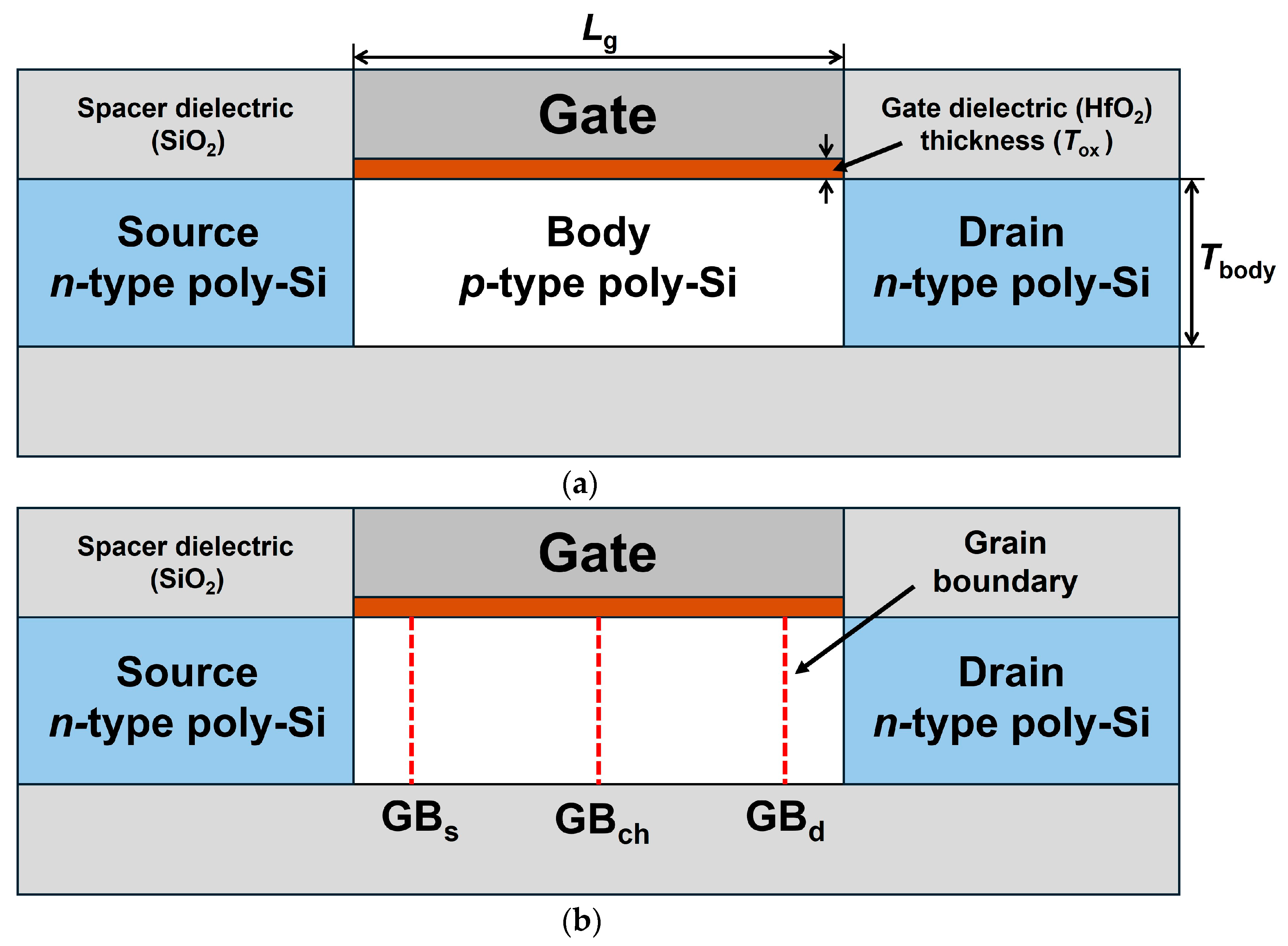
Figure 1. (a) A cross-sectional structure of the single-layer transistor and (b) GB locations in the device.
Electronics 14 03494 g001
Figure 2. GB trap distribution extracted from experimental data in [4].
Electronics 14 03494 g002
Figure 3. Transfer characteristics of a single-layer device at different temperatures under varying body doping concentration and grain boundary conditions.
Electronics 14 03494 g003
Figure 4. ZTC point dependence on body thickness for various GB locations: (a) without GB, (b) GBch, (c) GBs, (d) GBd.
Electronics 14 03494 g004
Figure 5. ZTC point sensitivity to GB locations: (a) GBch, (b) GBs, (c) GBd, and (d) evaluation of stability conditions.
Electronics 14 03494 g005aElectronics 14 03494 g005b
Figure 6. (a) A cross-sectional structure of the multi-layer transistor and (b) GB locations in the device.
Electronics 14 03494 g006
Figure 7. Evaluation of ZTC stability under different GB locations: (a) GBs at top, middle, and bottom, (b) GBtop, (c) GBmiddle, (d) GBbottom.
Electronics 14 03494 g007aElectronics 14 03494 g007b
Figure 8. Comparative analysis of ΔZTC in single-layer and multi-layer configurations with GB locations: (a) multi-layer with GBs at all layers and (b) multi-layer with a GB at a single layer.
Electronics 14 03494 g008
Table 1. Device parameters of the proposed single-layer transistor used for simulation.
ParametersValues
Gate length (Lg)70 nm
Body thickness (Tbody)7–25 nm
Gate dielectric (HfO2) thickness (Tox)3 nm
Source/Drain doping concentrationn-type, 5 × 1019 cm−3
Body doping concentrationp-type, 1 × 10¹⁶–1 × 1018 cm−3
Gate work function5.1 eV
Disclaimer/Publisher’s Note: The statements, opinions and data contained in all publications are solely those of the individual author(s) and contributor(s) and not of MDPI and/or the editor(s). MDPI and/or the editor(s) disclaim responsibility for any injury to people or property resulting from any ideas, methods, instructions or products referred to in the content.